Wideband transmission line - waveguide transition apparatus

a waveguide and transmission line technology, applied in electrical devices, waveguides, multiple-port networks, etc., can solve the problems of difficult direct connection of waveguide lines, high manufacturing costs, and difficulty in manufacturing waveguide lines formed by mechanical processing using metals

Inactive Publication Date: 2011-11-03
SAMSUNG ELECTRO MECHANICS CO LTD
View PDF3 Cites 47 Cited by
  • Summary
  • Abstract
  • Description
  • Claims
  • Application Information

AI Technical Summary

Benefits of technology

[0039]Besides, the quasi-cavity includes: one or more third conductive plates formed on the bottom of one or more dielectric layers among the plurality of dielectric layers; and a plurality of fourth metal via holes vertically penetrating a dielectric layer having one or more layers stacked on the one or more third conductive plates to form a vertical metallic surface by surrounding the one or more third conductive plates at a predetermined interval.
[0040]Further, the quasi-cavity is formed to decrease or increase the volume of the quasi-cavity formed at a portion of each of the plurality of dielectric layers step by step.

Problems solved by technology

Therefore, the waveguide line formed by mechanical processing using the metal is difficult to be manufactured and has high manufacturing cost due to its smaller size.
Further, in the device connection, it is difficult to directly connect the waveguide line and a universal subminiature A (SMA) or a transitioner using a via is generally used.
When the waveguide line is used as the low-loss transmission line, the biggest problem is that a band is narrowed by an impedance difference and a conversion loss is increased at the time of propagation-transitioning from the microstrip line or the coaxial line to the waveguide line.
Moreover, when a dielectric substrate is used in the millimeter wave band, a conversion characteristic from the microstrip line or the coaxial line to the waveguide line is further deteriorated by progress rate and properties of a substrate.
Accordingly, when the smaller the waveguide is, the higher the frequency is, forming the probe and the airline in the waveguide by the mechanical processing becomes difficult and the manufacturing cost is increased.
In this case, it is difficult to apply the known coaxial—waveguide transitioner structure to the dielectric substrate and a multi-layer substrate or a thin substrate.
However, even in such a method, while implementation using the dielectric substrate is possible, implementation using the metal waveguide is difficult, in the millimeter wave band.
Therefore, when sufficient thickness of the waveguide cannot be ensured due to a manufacturing or design condition, it is difficult to apply the above-mentioned known method.

Method used

View more

Image

Smart Image Click on the blue labels to locate them in the text.
Viewing Examples
Smart Image
  • Wideband transmission line - waveguide transition apparatus
  • Wideband transmission line - waveguide transition apparatus
  • Wideband transmission line - waveguide transition apparatus

Examples

Experimental program
Comparison scheme
Effect test

first embodiment

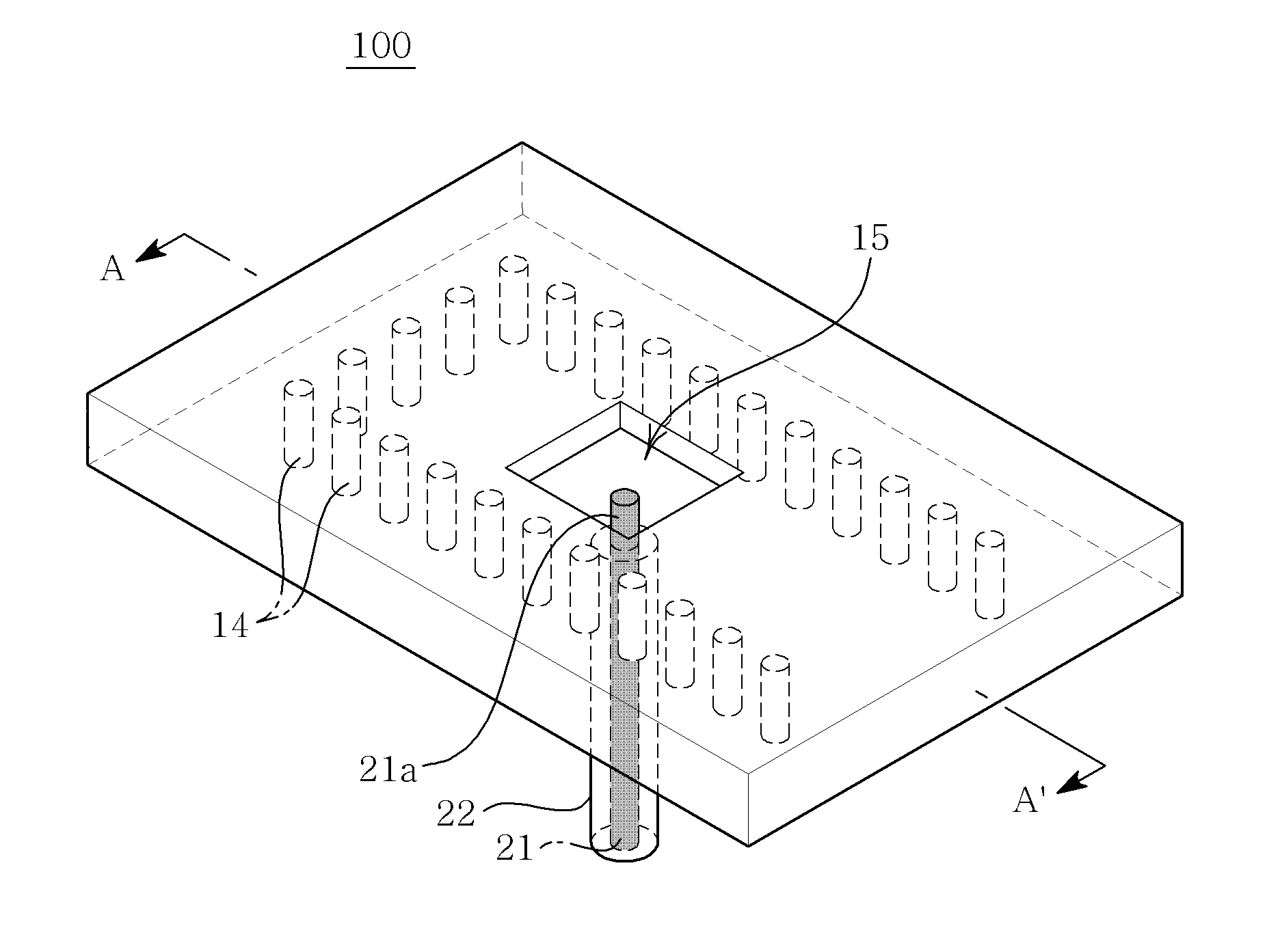
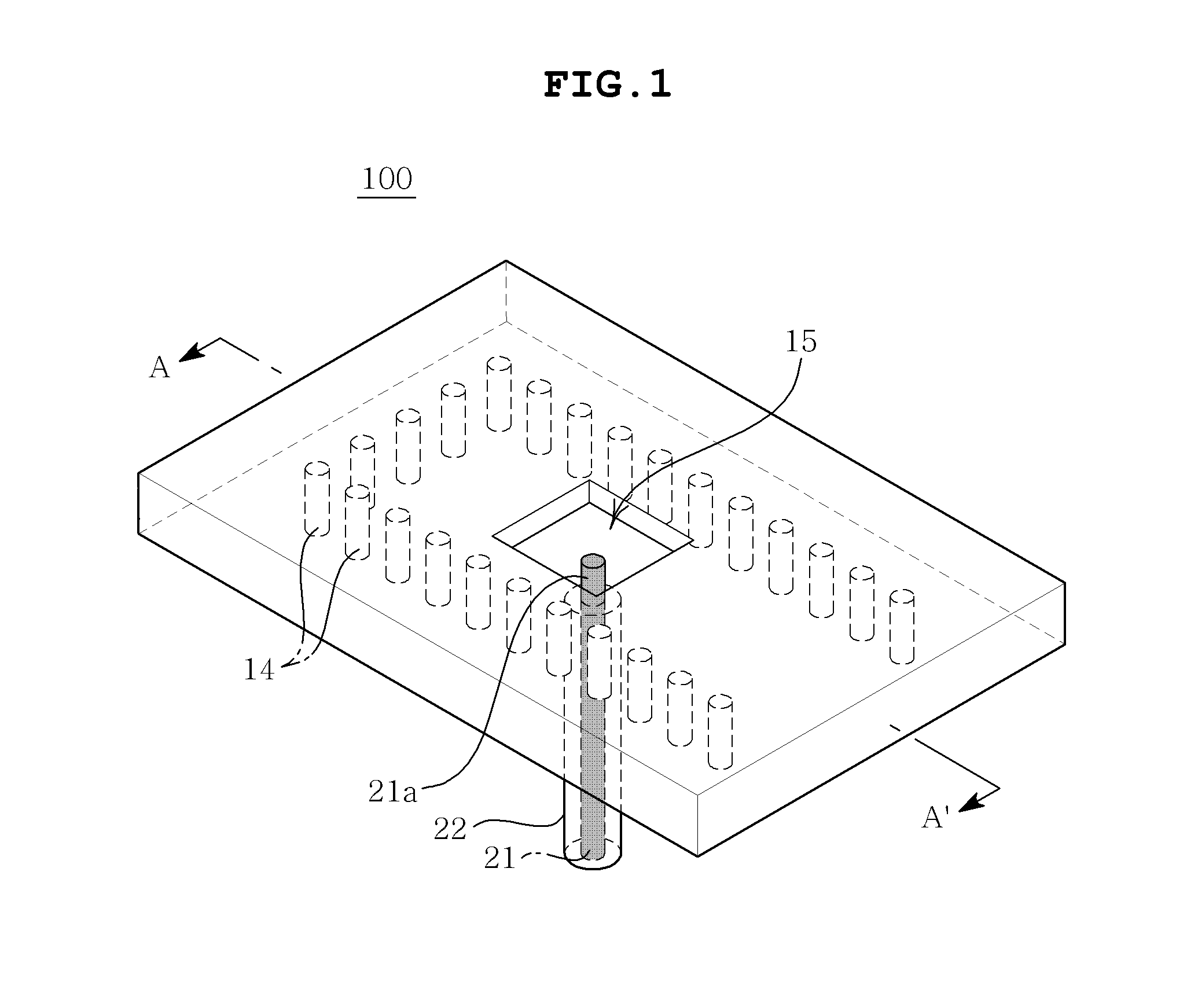
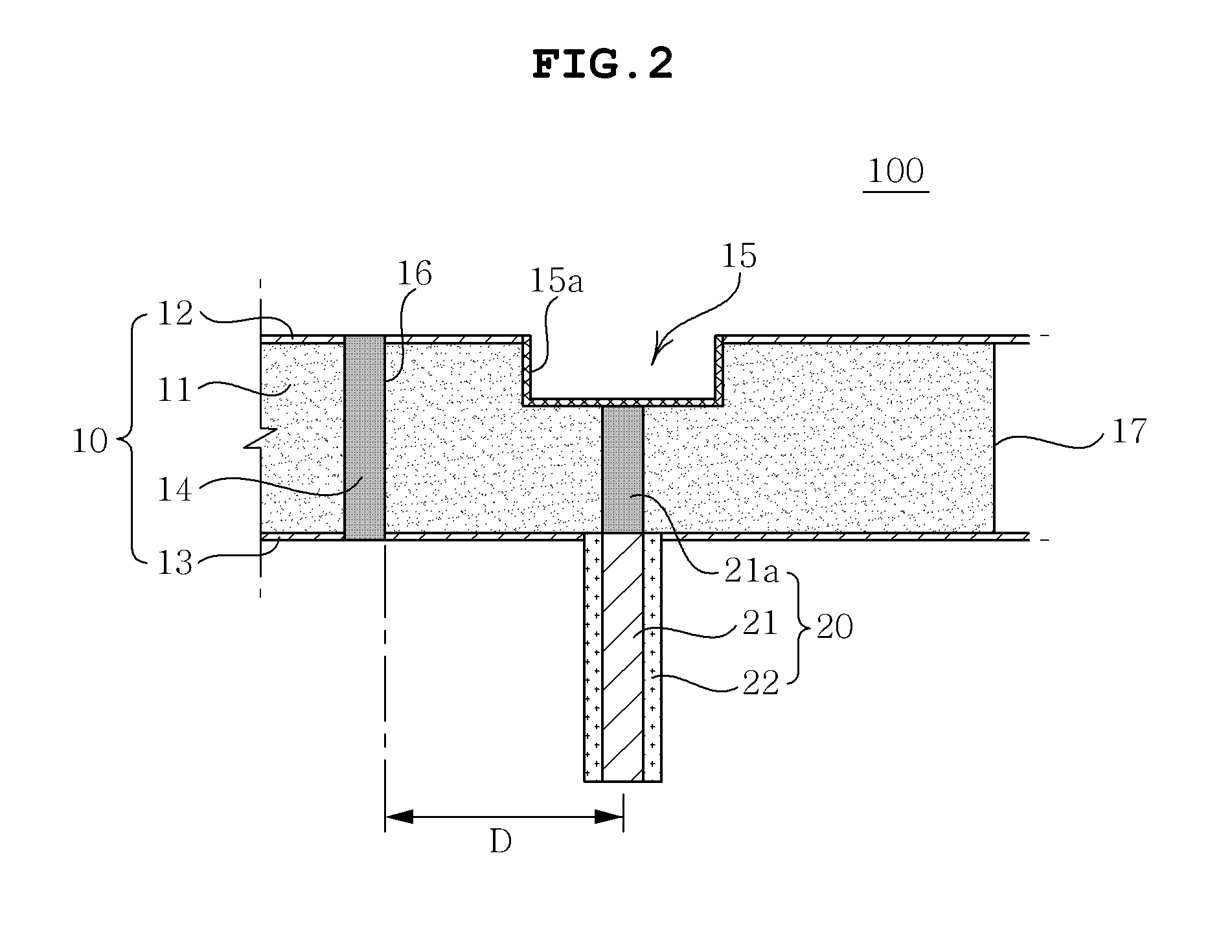
[0064]FIG. 1 is a schematic perspective view of a wideband transmission line—waveguide transition apparatus according to the present invention and FIG. 2 is a cross-sectional view of a wideband transmission line—waveguide transition apparatus taken along the line A-A′ of FIG. 1.

[0065]Referring to FIGS. 1 and 2, the wideband transmission line—waveguide transition apparatus 100 according to the first embodiment of the present invention includes a waveguide 10, a transmission line 20 that is inserted into the waveguide 10 to apply a to apply a signal, and a cavity matching unit 15 for impedance matching and phase matching between the waveguide 10 and the transmission line 20.

[0066]In the first embodiment of the present invention, a single dielectric waveguide is used as the waveguide 10.

[0067]The waveguide 10 includes a dielectric substrate 11 composed of one dielectric layer, a first conductive plate 12 formed on the top of the dielectric substrate 11, a second conductive plate 13 for...

second embodiment

[0079]FIG. 3 is a schematic perspective view of a wideband transmission line—waveguide transition apparatus according to the present invention and FIG. 4 is a cross-sectional view of a wideband transmission line—waveguide transition apparatus taken along the line B-B′ of FIG. 3.

[0080]The wideband transmission line—waveguide transition apparatus 200 according to the second embodiment of the present invention is the same as the wideband transmission line—waveguide transition apparatus 100 according to the first embodiment of the present invention shown in FIGS. 1 and 2 except for the structure of the cavity matching unit 15. Therefore, a detailed description of the same components will be substituted by the above description.

[0081]Referring to FIGS. 3 and 4, in the wideband transmission line—waveguide transition apparatus 200 according to the second embodiment of the present invention, an inner part of the cavity of the cavity matching unit 15 is filled with a predetermined metallic m...

third embodiment

[0086]FIG. 5 is a schematic perspective view of a wideband transmission line—waveguide transition apparatus according to the present invention and FIG. 6 is a cross-sectional view of a wideband transmission line—waveguide transition apparatus taken along the line C-C′ of FIG. 5.

[0087]Referring to FIGS. 5 and 6, the wideband transmission line—waveguide transition apparatus 300 according to the third embodiment of the present invention is the same as the wideband transmission line—waveguide transition apparatus 200 according to the second embodiment of the present invention shown in FIGS. 3 and 4 except for the waveguide 10. Therefore, a detailed description of the same components will be substituted by the above description.

[0088]In the third embodiment of the present invention, a multi-layer dielectric waveguide formed by stacking a plurality of dielectric layers 11a to 11d is used as the waveguide 10.

[0089]The waveguide 10 includes a dielectric substrate 11 formed by stacking the p...

Login to view more

PUM

No PUM Login to view more

Abstract

Disclosed herein is a wideband transmission line—waveguide transition apparatus. The wideband transmission line—waveguide transition apparatus includes: a waveguide constituted by a single dielectric substrate; a transmission line applying a signal to the waveguide; and a cavity matching unit in which a cavity of which an inner surface is formed by a metallic surface is formed at a portion of the waveguide to contact with the transmission line and impedance is adjusted through a change of the dielectric constant in the cavity caused by changing the size and shape of the cavity to perform impedance matching between the waveguide and the transmission line, and the position of the cavity is changed to perform phase matching between the waveguide and the transmission line.

Description

CROSS REFERENCE TO RELATED APPLICATION[0001]This application claims the benefit of Korean Patent Application No. 10-2010-0040863, filed on Apr. 30, 2010, entitled “Wideband Transmission Line—Waveguide Transition Apparatus”, which is hereby incorporated by reference in its entirety into this application.BACKGROUND OF THE INVENTION[0002]1. Technical Field[0003]The present invention relates to a wideband transmission line—waveguide transition apparatus.[0004]2. Description of the Related Art[0005]As a known transmission and receiving system, a product configuring a system by assembling separate parts is generally used. However, in recent years, a research of a system on package (SOP) product configuring a transmission and receiving system of a millimeter wave band by a single packet has been in progress and some products are being commercialized.[0006]As a high-efficient wideband transmission line in the millimeter wave band, a waveguide line is considered.[0007]The waveguide line has ...

Claims

Login to view more

Application Information

Patent Timeline
no application Login to view more
Patent Type & Authority Applications(United States)
IPC IPC(8): H01P5/103
CPCH01P5/103H01P3/121
Inventor LEE, JUNG AUN
Owner SAMSUNG ELECTRO MECHANICS CO LTD
Who we serve
  • R&D Engineer
  • R&D Manager
  • IP Professional
Why Eureka
  • Industry Leading Data Capabilities
  • Powerful AI technology
  • Patent DNA Extraction
Social media
Try Eureka
PatSnap group products