

Introduction: TDA2030 Amplifier Circuit 12v

The maximum voltage with standing by the TDA2030 amplifier is 36v, this is the reason why many changes are needed to build a 12v TDA2030 amplifier.
Step 1: Tda2030

TDA2030 amplifier circuit 12v, it is possible to operate the TDA2030 amplifier circuit in 12 volts, but we should follow the instruction to building properly functioned 12v TDA2030 amplifier
Step 2: Circuit Diagram and Working
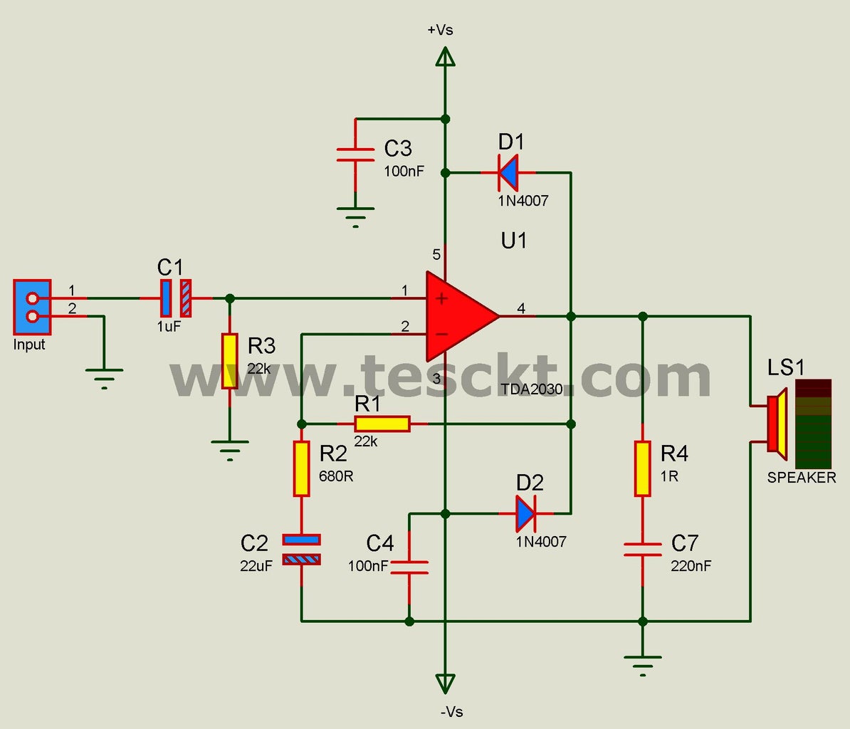
· TDA2030 IC had 5 pins, 1st pin non-inverting, 2nd pin inverting, 3rd -ve negative power pin, 4th output pin, and 5th +ve positive power pin.
· This is a single power supply circuit based Circuit, so the 3rd and 5th pin are connected to the power supply 12-volt dc. ·
When we connect our input signal towards the amplifier circuit, the C1 capacitor acts as the input DC coupling capacitor, it creates a division between signal incoming and R3 resistors are for to create an input impedance at the amplifier. ·
Non inverting pin is our input portion, at this portion R5 and R6 resistors and C6 capacitor, is for non-investing input action by R6 and R5 resistor, which is to attenuate poor higher frequency signals and C6 capacitor is for bypassing the over energy flow towards R6 resistor. ·
After non-inverting amplification, the signal reaches the output pin4, here we have D1 and D2 diodes for protection of the whole amplifier against the formation of voltage spikes, then the diodes are connected across both power supply ports such as pin5 and pin3. ·
Then after it reaches output, the amplifier needs negative feedback, it is done with components such as R1 and R2 resistors and C2 capacitor. R1, R2 resistor network set again using a closed-loop, the value difference of both resistors will cause gain changing at the output. ·
Whole feedback network works using our inverting pin2, so the C2 capacitor is for decoupling DC current at the inverting portion. ·
And at the output we have a C5 Capacitor for supply voltage bypassing and an R4 resistor stabilizing the frequency of the amplified signal, and then C7 capacitor acts as a stabilizing supporting agent combined with an R4 resistor. ·
Last is our two capacitors such as C8 and C3, they are bypassing capacitors, the C8 capacitor is to bypass upper-frequency purpose and the C4 capacitor is the supply voltage bypassing capacitor.
Step 3: Pcb Layout
you will have to need more details about this circuit please visit my website tesckt.com


