Table of Contents
Advertisement
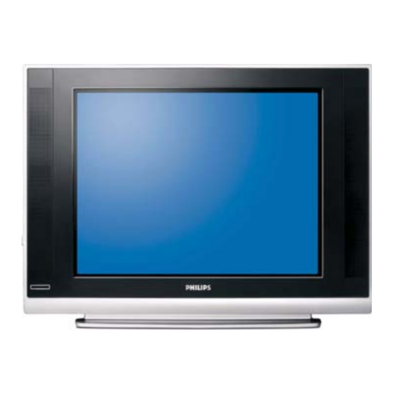
Colour Television
©
Copyright 2007 Philips Consumer Electronics B.V. Eindhoven, The Netherlands.
All rights reserved. No part of this publication may be reproduced, stored in a
retrieval system or transmitted, in any form or by any means, electronic,
mechanical, photocopying, or otherwise without the prior permission of Philips.
Published by JY 0768 BU CD Customer Service
Contents
Waveforms
Printed in the Netherlands
29PT9457/55
Page
2
4
5
6
9
10
(A1) 11
19-20
(A2) 12
19-20
(A3) 13
19-20
(A4) 14
19-20
(A5) 15
19-20
(A6) 16
19-20
(A7) 17
19-20
(A8) 18
19-20
(B) 21
19-20
23
24
(G) 25
25
29
34
35
36
51
54
Subject to modification
Chasis
SK5.0L
CA
H_17220_000.eps
210607
EN 3122 785 17460
Advertisement
Table of Contents

Related Manuals for Philips SK5.0L CA


Summary of Contents for Philips SK5.0L CA
-
Page 1: Table Of Contents
All rights reserved. No part of this publication may be reproduced, stored in a retrieval system or transmitted, in any form or by any means, electronic, mechanical, photocopying, or otherwise without the prior permission of Philips. Published by JY 0768 BU CD Customer Service... -
Page 2: Technical Specifications, Connections, And Chassis Overview
EN 2 SK5.0l CA Technical Specifications, Connections, and Chassis Overview 1. Technical Specifications, Connections, and Chassis Overview Connection Overview Index of this chapter: 1.1 Technical Specifications 1.2 Connection Overview Note: The following connector colour abbreviations are used 1.3 Chassis Overview (Mechanical chassis) (acc. - Page 3 Technical Specifications, Connections, and Chassis Overview SK5.0l CA EN 3 Chassis Overview (Mechanical chassis) CRT BOARD MAINS FILTER CONTROL PANEL POWER SUPPLY LINE DEFLECTION FRAME DEFLECTION TUNER IF MONO CARRIER AV SWITCH TONE CONTROL BTSC PANEL AUDIO AMPLIFIER CPU & DECODER SIDE AV PANEL H_17220_024.eps...
-
Page 4: Safety Instructions, Warnings, And Notes
EN 4 SK5.0l CA Safety Instructions, Warnings, and Notes 2. Safety Instructions, Warnings, and Notes Index of this chapter: 1. Perform the “general repair instruction” noted above. 2.1 Safety Instructions 2. Clean the power supply and deflection circuitry on the 2.2 Maintenance Instructions... -
Page 5: Directions For Use
• Resistor values with no multiplier may be indicated with In September 2003, Philips CE introduced a change in the way either an "E" or an "R" (e.g. 220E or 220R indicates the serial number (or production number, see Figure 2-2) is 220 ohm). -
Page 6: Mechanical Instructions
EN 6 SK5.0l CA Mechanical Instructions 4. Mechanical Instructions Index of this chapter: 4.1.1 Rear Cover Removal 4.1 Set Disassembly 4.2 Assembly / Board Removal Warning: disconnect the mains power cord before you remove 4.3 Set Re-assembly the rear cover. - Page 7 Mechanical Instructions SK5.0l CA EN 7 4.2.2 Side I/O Panel removal H_17220_023.eps 210607 Figure 4-3 Side-I/O panel removal 1. Disconnect the side panel cable from the mono carrier and remove the cable from it’s strain reliefs. 2. Then, remove the four fixation screws [1] and remove the board.
-
Page 8: Service Modes, Error Codes, And Fault Finding
EN 8 SK5.0l CA Service Modes, Error Codes, and Fault Finding 5. Service Modes, Error Codes, and Fault Finding Index of this chapter: 5.4.6 Picture not or incorrect Coloured 5.1 Test Points 5.2 Service Modes • Check the circuit from IC201 to R.G.B. three gun circuit. -
Page 9: Block Diagrams, Test Point Overview, And
Block Diagrams, Test Point Overview, and Waveforms SK5.0L CA EN 9 6. Block Diagrams, Test Point Overview, and Waveforms Block Diagram Chassis H_17460_008.eps 280907... -
Page 10: Schematic Overview Chassis
Block Diagrams, Test Point Overview, and Waveforms SK5.0L CA EN 10 Schematic Overview Chassis KEYBOARD CIRCUIT R516 R515 D504 M001 H501 Q506 BA158 BF420 U101 R510 Q504 C4544 45.75MHz Q505 L109 +8V_VCC MENU BF421 R511 R513 R512 R517 10uF/16V 100uH... -
Page 11: Circuit Diagrams And Pwb Layouts
Circuit Diagrams and PWB Layouts SK5.0L CA EN 11 7. Circuit Diagrams and PWB Layouts Mono Carrier: Power Supply POWER SUPPLY R640 D627 RL601 C640 Q625 R644 1N4148 C1815 RELAY 220uF R643 C639 47uF C603A C603B T601 4700pF 4700pF C624... -
Page 12: Mono Carrier: Line Deflection (A2)
Circuit Diagrams and PWB Layouts SK5.0L CA EN 12 Mono Carrier: Line Deflection LINE DEFLECTION CN401 CN301 TO CRT H-DEF R413 100K D404 ZD402 R421 X-ray X-ray 1N4148 R412 R422 R418 R423 C407 3.9 2W T402 R450 HV TO CRT +13V 0.22... -
Page 13: Mono Carrier: Frame Deflection (A3)
Circuit Diagrams and PWB Layouts SK5.0L CA EN 13 Mono Carrier: Frame Deflection FRAME DEFLECTION CN301 IC301 TDA4863AJ 100V C456 R461 5.6 1/4W VDRA C455 0.1uF/100V R460 VDRA 100V R453 100uF/50V 270 1W R457 R452 VDRB D452 VDRB J408 BA158... -
Page 14: Mono Carrier: Tuner If (A4)
Circuit Diagrams and PWB Layouts SK5.0L CA EN 14 Mono Carrier: Tuner IF TUNER IF U101 38.9MHz R104 C103 10nF R116 R106 L101 R107 R103 C111 C113 C112 R111 C110 R113 R112 5.1K C405 C109 C105 100pF 100pF C101 10uF... -
Page 15: Mono Carrier: Av Switch (A5)
Circuit Diagrams and PWB Layouts SK5.0L CA EN 15 Mono Carrier: AV Switch... -
Page 16: Mono Carrier: Tone Control (Optional) (A6)
Circuit Diagrams and PWB Layouts SK5.0L CA EN 16 Mono Carrier: Tone Control (Optional) TONE CONTROL R OUT L OUT IC740 TDA9859 LOUT_L LOUT_R C_TL C_TR N.C. N.C. C_BL2 C_BR2 C_BL1 C_BR1 LIN_L LIN_R MOUT_L MOUT_R SCOUT_L SCOUT_R C_PS2 AIN_L... -
Page 17: Mono Carrier: Audio Amplifier (A7)
Circuit Diagrams and PWB Layouts SK5.0L CA EN 17 Mono Carrier: Audio Amplifier AUDIO AMPLIFIER IC760 +8V_VCC +8V_VCC TFA9843AJ---10W TFA 9842AJ---6W D763 IN4148 C728 L in L out 100uF R768 R766 Q760 100K A1015 C767 C764 220uF C769 CN760 47uF... - Page 18 Circuit Diagrams and PWB Layouts SK5.0L CA EN 18 Mono Carrier: CPU & Decoder CPU & DECODER R120 C118 C117 ZD102 IC102 100uF/16V C108 R132 100nF C107 R130 R131 R145 24C08 3.3K R121 100pF 3.3K 3.3K 100pF Q106 C1815 R149 R148 3.3K...
-
Page 19: Mono Carrier: Cpu & Decoder (A8)
Circuit Diagrams and PWB Layouts SK5.0L CA EN 19 Layout Mono Carrier (Top Side) H_17220_011.eps 280607 5800-A5P190-00... - Page 20 Circuit Diagrams and PWB Layouts SK5.0L CA EN 20 Layout Mono Carrier (Bottom Side) H_17220_012.eps 5800-A5P190-00 280607...
-
Page 21: Crt Board (B)
Circuit Diagrams and PWB Layouts SK5.0L CA EN 21 CRT Board CRT BOARD R516 R515 D504 H501 Q506 BA158 BF420 R510 Q504 C4544 Q505 BF421 R517 R512 R511 R513 R514 R527 C502 D503 470PF 1N4148 R508 ZD501 C508 R526 82PF... - Page 22 Circuit Diagrams and PWB Layouts SK5.0L CA EN 22 Keyboard Control Panel KEY CONTROL KEYBOARD CIRCUIT KEYBOARD CIRCUIT M001 MENU 10uF/16V VOL+ VOL- PRO+ PRO- SW004 SW003 SW002 SW001 +5V_VCC H_17220_014.eps 5800-D9SL7Y-05 190607...
-
Page 23: Keyboard Control Panel
Circuit Diagrams and PWB Layouts SK5.0L CA EN 23 Layout Keyboard Control Panel (Top Side) Layout Keyboard Control Panel (Bottom Side) H_17220_038.eps 5800-D9SL7Y-05 5800-D9SL7Y-05 H_17220_015.eps 290607 190607... -
Page 24: Mains Filter Panel
Circuit Diagrams and PWB Layouts SK5.0L CA EN 24 Mains Filter Panel Layout Mains Filter (Top Side) MAINS FILTER C603A C603B T601 4700pF 4700p F C603 0.22uF PTC601 D603 AC250V CN604 C603D C603C C607 FOR CB CN602 FOR EMC R600... -
Page 25: Side A/V Panel (G)
Circuit Diagrams and PWB Layouts SK5.0L CA EN 25 Side A/V Panel Layout Side A/V Panel Side AV Top Layer Side AV Panel S-VHS P702 C785 10uF ZD707 R779 P701 Side AV Bottom Layer C777 V IN 10uF C772 L IN... - Page 26 Circuit Diagrams and PWB Layouts SK5.0L CA EN 26 BTSC Panel BTSC BOARD IC851 FOR LATAM TDA9850 R852 C862 C863 R853 C861 C864 47nF C860 10uF 10uF C809 C865 0.1uF 10uF C866 Cdec 4.7uF C872 AGND OUTL C867 DGND 0.1uF...
- Page 27 Circuit Diagrams and PWB Layouts SK5.0L CA EN 27 Layout BTSC Panel (Top Side) Layout BTSC Panel (Bottom Side) 5800-M5P190-00 H_17460_004.eps 5800-M5P190-00 5800-M5P190-00 H_17460_005.eps 240907 240907...
- Page 28 Circuit Diagrams and PWB Layouts SK5.0L CA EN 28 Personal Notes: E_06532_013.eps 131004...
-
Page 29: Alignments
Alignments SK5.0L CA EN 29 8. Alignments Index of this chapter: 8.3.3 Screen Voltage Adjust 8.1 General Alignment Conditions 8.2 Hardware Alignments 1. Set picture to “Standard” mode, without signal input. 8.3 Software Alignments 2. Press the keys [i+], “Smart sound” and “Smart picture” to 8.4 Factory mode Settings... - Page 30 EN 30 SK5.0L CA Alignments Enter Factory Mode: Press sequentially: ---> Smart Sound ---> Smart Picture Main Menu in red box. Navigation: Navigate parameters in "Main Page" : From the first menu, use the arrow Up or Down to navigate to different pages.
- Page 31 Alignments SK5.0L CA EN 31 Factory mode Settings Description of the factory menu Storage address Display string Range (Index value) Default SK5.0L CA B/W balance White point R adjustment. DRI R 0-63 0x00d White point G adjustment 0x00e DRI G...
- Page 32 EN 32 SK5.0L CA Alignments Description of the factory menu Storage address Display string Range (Index value) Default SK5.0L CA Volume of 9859 modify value when sound is stereo 0x053 STEREO GAIN 0-63 Volume of 9859 modify value when sound is SAP...
- Page 33 Alignments SK5.0L CA EN 33 Description of the factory menu Storage address Display string Range (Index value) Default SK5.0L CA SUB SHA Sub Sharpness 0x024 0-63 SUB TIN TV Sub tint 0x025 0-31 SUB TIN-AV AV Sub tint 0x075 0-31...
-
Page 34: Circuit Descriptions, Abbreviation List, And Ic Data Sheets
The composite signal is fed from the output of the input level adjustment stage to the SAP demodulator circuit through a 5fH The SK5.0L CA is a CRT TV for the year 2007, based on the band-pass filter. The demodulator level is automatically 5P19 platform. -
Page 35: Abbreviation List
Circuit Descriptions, Abbreviation List, and IC Data Sheets SK5.0L CA EN 35 Abbreviation List H-FLYBACK Horizontal Flyback H-OUT H_sync output of the module / Horizontal Output pulse 2 Carrier Sound Horizontal Acquisition; horizontal sync Commonly known as 2 Carrier Sound... -
Page 36: Ic Data Sheets
EN 36 SK5.0L CA Circuit Descriptions, Abbreviation List, and IC Data Sheets can directly provide the desired IC Data Sheets frequency Progressive Scan Scan mode where all scan lines are This section shows the internal block diagrams and pin layouts displayed in one frame at the same of ICs that are drawn as “black boxes”... - Page 37 Circuit Descriptions, Abbreviation List, and IC Data Sheets SK5.0L CA EN 37 9.4.1 Diagram A1, W6554A, (IC601) H_17210_039.eps 120607 Figure 9-1 Block Diagram and Pin Configuration...
- Page 38 EN 38 SK5.0L CA Circuit Descriptions, Abbreviation List, and IC Data Sheets 9.4.2 Diagram A1, P412, (IC602) H_17210_039.eps 120607 Figure 9-2 Block Diagram and Pin Configuration...
-
Page 39: Pin Configuration
Circuit Descriptions, Abbreviation List, and IC Data Sheets SK5.0L CA EN 39 9.4.3 Diagram A3, TDA486x, (IC301) Block Diagram TDA4865AJ THERMAL PROTECTION DIFFERENTIAL VERTICAL FLYBACK REFERENCE INPUT OUTPUT GENERATOR CIRCUIT STAGE VOUT R S1 C S1 deflection coil from deflection controller... - Page 40 EN 40 SK5.0L CA Circuit Descriptions, Abbreviation List, and IC Data Sheets H_17210_035.eps 120607 Figure 9-4 Block Diagram...
- Page 41 Circuit Descriptions, Abbreviation List, and IC Data Sheets SK5.0L CA EN 41 9.4.4 Diagram A5, 4052, (IC102) Block Diagram Pin Configuration H_17210_041.eps 120607 Figure 9-5 Block Diagram and Pin Configuration...
- Page 42 EN 42 SK5.0L CA Circuit Descriptions, Abbreviation List, and IC Data Sheets 9.4.5 Diagram A7, TDA9842, (IC402) Block Diagram OUT1 kΩ OUT2 kΩ SHORT-CIRCUIT TEMPERATURE V REF PROTECTION VOLUME CONTROL 0.5V TFA9842AJ Pin Configuration OUT2 TFA9842AJ OUT1 H_17210_033.eps 110607 Figure 9-6 Block Diagram and Pin Configuration...
- Page 43 Circuit Descriptions, Abbreviation List, and IC Data Sheets SK5.0L CA EN 43 9.4.6 Diagram A7, TDA9850, (IC801) Block Diagram ceramic resonator L + R stereo OUTL mono DEMATRIX STEREO DECODER MODE L − R/SAP audio SELECT OUTR processing TDA9850 INPUT...
- Page 44 EN 44 SK5.0L CA Circuit Descriptions, Abbreviation List, and IC Data Sheets 9.4.7 Diagram A8, OM837x (IC201) Block Diagram H_17210_034.eps 130607 Figure 9-8 Block Diagram...
- Page 45 Circuit Descriptions, Abbreviation List, and IC Data Sheets SK5.0L CA EN 45 Pin Configuration H_17210_029.eps 130607 Figure 9-9 Pin Configuration...
- Page 46 EN 46 SK5.0L CA Circuit Descriptions, Abbreviation List, and IC Data Sheets H_17210_030.eps 130607 Figure 9-10 Pin Configuration...
- Page 47 Circuit Descriptions, Abbreviation List, and IC Data Sheets SK5.0L CA EN 47 Pinning H_17210_031.eps 130607 Figure 9-11 Pin Configuration...
- Page 48 EN 48 SK5.0L CA Circuit Descriptions, Abbreviation List, and IC Data Sheets 9.4.8 Diagram A8, TDA937x (IC201) Block Diagram SOUND TRAP +3.3 V TUNERAGC IFVO/SVO VISION IF QSS SOUND IF C-BUS ENHANCED ALIGNMENT-FREE TRANSCEIVER IFIN MEMORY PLL DEMOD. 80C51 CPU...
- Page 49 Circuit Descriptions, Abbreviation List, and IC Data Sheets SK5.0L CA EN 49 9.4.9 Diagram A8, 24C08 (IC202) H_17210_035.eps 120607 Figure 9-13 Block Diagram...
- Page 50 EN 50 SK5.0L CA Circuit Descriptions, Abbreviation List, and IC Data Sheets Pin Configuration H_17210_036.eps 120607 Figure 9-14 Pin Configuration...
-
Page 51: Spare Parts List
Spare Parts List SK5.0L CA EN 51 10. Spare Parts List CTN’s Listed: C162 9965 000 40529 33pF 50V C745 9965 100 05389 0.068μF 10% 100V C402 9965 000 40164 0.0022μF 500V C746 9965 100 05387 0.15μF 5% 100V C403... - Page 52 9965 000 40596 TDA9859 R461 9965 000 39985 CFR 5.6Ω R768 9965 100 05150 91kΩ 5% 1/4W IC760 9965 100 04917 TFA9842AJ PHILIPS R462 9965 100 05312 0.82Ω 2W R769 9965 000 40304 CFR 1KΩ 1/16W IC761 9965 000 40309 HCF4052BF SGS R463 9965 000 40138 MOFR 220Ω...
- Page 53 Spare Parts List SK5.0L CA EN 53 C001 9965 000 40529 33pF 50V 9965 100 04879 10μF 20% 10V 9965 000 39986 CFR 10Ω 1/4W 9965 000 40003 CFR 2.7kΩ 9965 000 39987 CFR 100Ω 9965 000 40489 CFR 18kΩ 1W 9965 000 39989 CFR 10kΩ...
-
Page 54: Revision List
EN 54 SK5.0L CA Revision List 11. Revision List Manual xxxx xxx xxxx.0 • First release.