A Cyclic Vernier Two-Step TDC for High Input Range Time-of-Flight Sensor Using Startup Time Correction Technique


School of Electronics and Information, Information and Communication System-on-chip (SoC) Research Center, Kyung Hee University, Yongin 17104, Korea
*
Author to whom correspondence should be addressed.
Sensors 2018, 18(11), 3948; https://doi.org/10.3390/s18113948
Submission received: 12 October 2018
/
Revised: 9 November 2018
/
Accepted: 11 November 2018
/
Published: 15 November 2018
(This article belongs to the Section Physical Sensors)
Abstract
:Herein, we present a low-power cyclic Vernier two-step time-to-digital converter (TDC) that achieves a wide input range with good linearity. Since traditional approaches require a large area or high power to achieve an input range >300 ns, we solve this problem by proposing a simple yet efficient TDC suitable for time-of-flight (TOF) sensors. In previous studies using the cyclic structure, the effect of startup time on the linearity of the TDC is not described. Thus, the achievable linearity has been limited when the TDC is used for applications requiring a high input range. We solve this problem by using a simple yet effective technique to compensate. The proposed technique is realized using (1) digitally-controlled oscillators (DCOs) that have dual frequency control and matched startup time; (2) an alignment detector that performs startup time correction by proper timing control; and (3) a fully symmetric arbiter that precisely detects the instant of edge alignment. To achieve a fine resolution for the cyclic Vernier TDC, we design two closely-matched DCOs with dual frequency control. The alignment detector performs the critical task of cancelling startup time via timing control. The detector is delay-compensated by using a dummy to provide matched loading for the two DCOs. To enhance the detection speed under low power, a current-reuse approach is employed for the arbiter. The TDC is fabricated using a 0.18 μm complementary metal–oxide–semiconductor (CMOS) process in a compact chip area of 0.028 mm2. Measured results show a dynamic range of 355 ns and a resolution of 377 ps. When the result is applied for TOF sensing, it corresponds to a distance range of 53.2 m and a resolution of 5.65 cm. Over a relatively large input range, good linearity is achieved, which is indicated by a DNL of 0.28 LSBrms and an INL of 0.96 LSBrms. The result corresponds to root mean square (RMS) error distance of 5.42 cm. The result is achieved by consuming a relatively low power of 0.65 mW.
1. Introduction
A time-to-digital converter (TDC) is widely used to quantize and digitize time interval information and regarded as one of the most important time sensor [1]. The time interval between pulse signals is used for various sensing applications, for example, altitude sensing [2], depth sensing [3], respiration rate sensing [4], biomedical image sensing [5,6], and distance sensing for navigation [7].
In reference [2], a TDC is integrated with the single-photon avalanche diodes (SPAD) to form the pixel of the sensor, which is used for the image sensor in short-range and for altimeters in the long-range applications. For image sensing applications, time-of-flight (TOF) measurements estimate the shape of an object by measuring the distance between the sensor pixels and the target object [3]. For biomedical sensing applications, the fluorescence lifetime image (FLIM) sensor uses TDCs to extract important information for identifying cell microstructure [5], which is not usually available from intensity image sensing. TDCs also have great utility in positron emission tomography (PET) image sensing [6]. In reference [7], a TDC is integrated into a distance sensing system for providing range information.
Recently, challenging direct time-of-light (dTOF) applications have been reported using the SPAD equipped with high-performance TDCs. In reference [8], a technique to detect objects hidden from view and track them in real time is presented with a TDC having a 45.5 ps temporal resolution. In reference [9], a massively parallel FLIM microscope for live-cell FRET (Förster resonance energy transfer) imaging is presented with 52.5 +/− 0.7 ps resolution. In reference [10], a confocal non-line-of-sight (NLOS) imaging technique is presented to address the challenge of reconstructing the shape of hidden objects from extremely weak and multiply scattered light. Using a TDC having 4 ps resolution, this work achieves a precision up to 15.1 mm in 0.64 m distance. In reference [11], a depth and reflectivity imaging system with a 390 ps resolution single-photon camera is presented, which achieves high photon efficiency by exploiting both the transverse smoothness and longitudinal sparsity of natural scenes. Although these imaging system using dTOF are widely rely on TDCs, the depth imaging can also be realized using a time-gated image sensor, which achieves a relatively high fill-factor of 61% [12]. Imaging hidden objects are crucial in a diverse area of applications such as robot vision, medical diagnostics, remote sensing, and autonomous vehicles.
Thanks to the advantage of high speed and massive integration available with CMOS scaling, a modern sensor with monolithic integrated TDC has become a preferred approach [13,14]. Fast digital switching capability allows extracting fine time resolution and TDCs are realized using deep-submicron CMOS [15,16]. Because the operation of SPAD requires a high voltage, however, the imaging system is not usually realized in deep-submicron standard CMOS process. Another issue for integrated CMOS imaging system is that the SPAD pixel arrays usually suffer from a low fill-factor, which is attributed to the large area engaged with timing electronics. To overcome the drawback, techniques to integrate diffractive microlens arrays are presented for the SPAD fabricated using 0.35 μm high-voltage (HV) CMOS process [17,18]. In reference [19], the SPAD are realized in ultrathin-body silicon-on-insulator (SOI) process, which allows both frontside-illumination (FSI) backside-illumination (BSI) modes. The BSI mode allows imaging with a wide carrier region which is not blocked by metallization, achieving a virtually perfect fill factor.
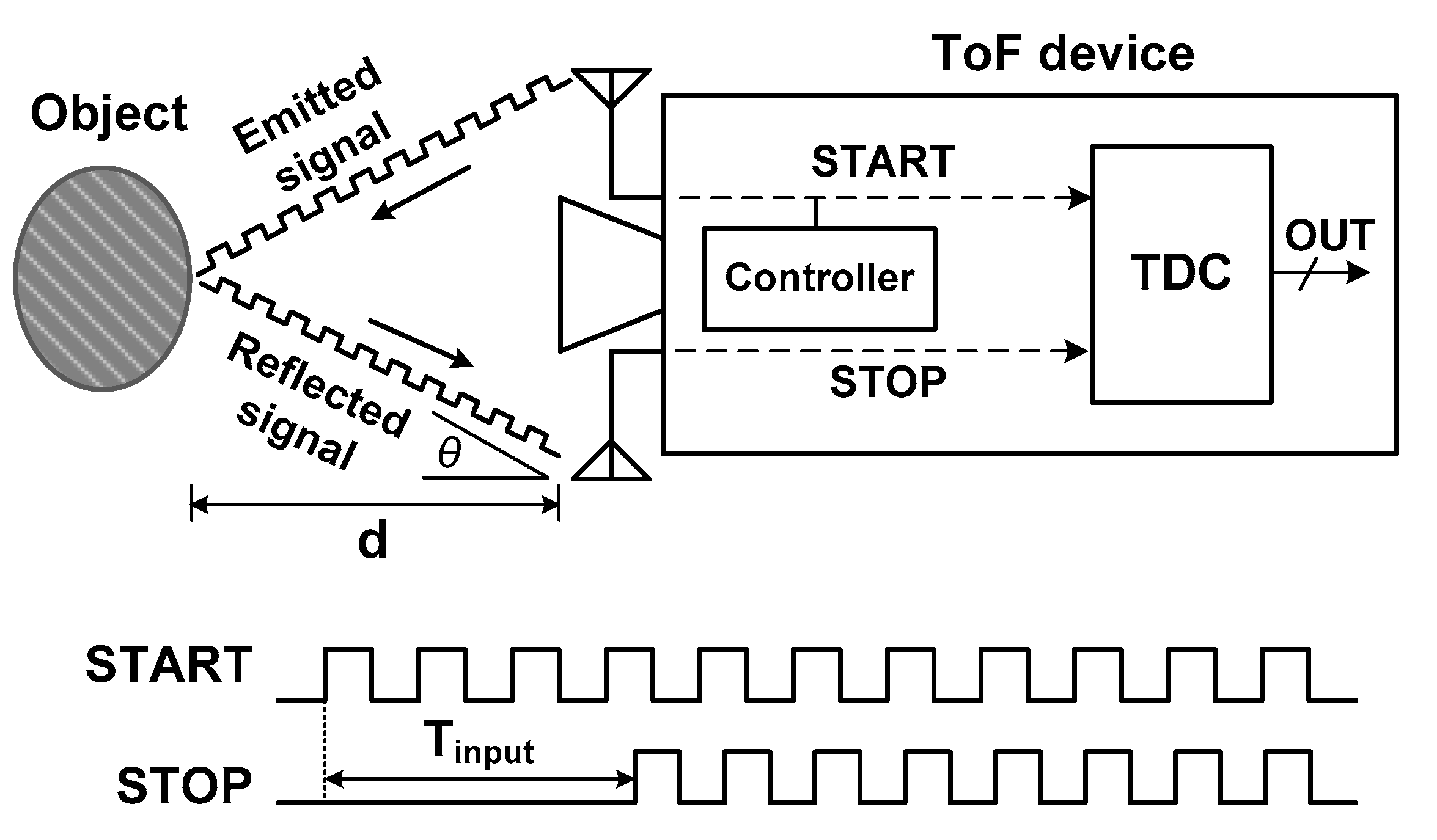
For those sensing devices using the TDC, the operating principle is based on the TOF technique. Figure 1 shows the basic operation of a TOF sensing device. The sensor emits a signal with a known time reference and measures the reflected signal from an object. When the time difference Tinput between signal emission (START) and detection (STOP) is measured, the distance d between the device and object is estimated using
where c is the speed of the light and θ is the angle between the device and the object. If d is very large compared to the size of the device, θ is almost zero, leading to d = c × Tinput/2.
When a TOF sensor or a 3D camera is used to measure the distance or object’s surface depth, its range is directly related to the input range of the TDC [7]. Therefore, a high input range is desirable for many such sensing applications. For example, a high input range with fine resolution allows a camera to sense realistic shapes and surface textures of objects. Because long-time measurements are adversely affected by accumulated jitter and mismatch-related nonlinearity, realizing a sensor achieving a large input range is challenging [15]. Various strategies are reported to increase input range while achieving fine resolution, including two-dimensional (2-D) and three-dimensional (3-D) Vernier structure [16,20], cyclic Vernier [21], gated-Vernier oscillator [22], and a time-to-voltage converter (TVC) [23].
The Vernier TDC uses two delay lines to measure sub-gate delay or time delay smaller than the delay allowed by the process technology. Although this approach has the advantage of a simple implementation, the mismatch between the delay elements limits the achievable resolution. An improved approach involves replacing one of the delay lines with a delay latch chain [24]. This approach saves power and area in addition to reducing the mismatch of the conventional structure. However, the Vernier structure has an intrinsic limit for the achievable input range. This is because the range can only be extended by increasing the number of delay elements. To solve this problem, an interpolation technique is proposed [25], which is based on the Nutt method [26]. Another approach to reducing the length of the delay line involves extending the conversion dimension [16,20]. The 3D approach uses a delay line for the coarse step and a 2D Vernier plane for the fine step [20]. This approach achieves a moderate input range of 14 ns by using a relatively large area of 0.21 mm2.
Another approach used to extend the performance of the TDC is using a time-to-voltage converter (TVC) followed by a successive approximation register (SAR) analog-to-digital converter (ADC) [23]. This approach converts the time interval into a voltage, and then quantizes the voltage by the ADC. In this approach, the design of a TVC with a high gain (for a full input range of the ADC) and linearity is challenging. Another drawback to this approach is the large area needed for the on-chip capacitors of the SAR ADC.
The limit of the Vernier delay line for high input range can be solved by using a ring structure for time quantization. In this cyclic Vernier architecture, the two delay lines are replaced with two oscillators which have slightly different frequencies [21,22]. The work in [21] synthesizes a cyclic TDC using the standard cell library and achieves 5.5 ps resolution. The systemic mismatch of the oscillator delay, which is generated by automatic place-and-route, is handled by measuring and calibrating the buffer delay. The ring oscillator is, however, rather sensitive to the process-voltage-temperature (PVT) variation. To handle PVT variation, a gated-Vernier oscillator is proposed [22]. By the first-order noise shaping, the effect of PVT variation and layout mismatch in the oscillator is reduced; the achieved input range of 20 ns is not suitable for TOF applications that demand a large input range.
To achieve a large input range, one can simply try to increase the number of bits of the counter. When the number of bits is increased, however, clock cycles integrate more jitter, which compromises linearity. As such, this approach is suboptimal as it suffers from degraded linearity and requires increased power. Another important design consideration for cyclic TDCs is the startup time, Tstartup, of an oscillator. The approach using the STOP signal to directly control the counter, which measures the number of oscillation cycles, cannot compensate for the delay caused by Tstartup, resulting in counting errors. For applications demanding a large input range, the error caused by Tstartup has a significant impact on linearity [27].
Since traditional approaches [16,20,25], require a large area or high power to achieve a large input range, we solve this problem by using a simple yet efficient TDC suitable for TOF applications. In the previous studies using cyclic structure [21,25,28], the effect of Tstartup on the linearity of the TDC is not investigated. Thus, the achievable linearity has been limited when the TDC is used for applications requiring an input range >300 ns. We solve this problem by using a technique to remove the Tstartup error.
To meet the demands of TOF applications which require the input range from sub-nanoseconds to hundreds of nanoseconds [7], herein, we present a low-power cyclic Vernier two-step TDC achieving good linearity over a wide input range. The TDC is realized using (1) digitally-controlled oscillators (DCOs) with dual frequency control and matched Tstartup; (2) a new alignment detector performing Tstartup correction via proper timing control; and (3) a fully symmetric arbiter performing precise detection of the instant of edge alignment. To compensate for the delay caused by Tstartup, the alignment detector controls the counters with proper timing instead of using the STOP signal. By the proposed technique, the error caused by Tstartup is effectively removed by measuring Tinput from the time difference between two closely-matched DCOs. The experimental results show that the proposed Tstartup correction achieves a good linearity over a relatively wide input range of 355 ns. When the result is applied to TOF range sensor, it corresponds to a detection range of 53.2 m and a resolution of 5.65 cm. Over the input range, good linearity is indicated by a differential nonlinearity (DNL) of 0.28 LSBrms (root mean square of the least significant bit) and an integral nonlinearity (INL) of 0.96 LSBrms. When the INL is used to indicate the discrepancy between the measured and real distance [20], the corresponding error distance is about 5.42 cm.
2. Design
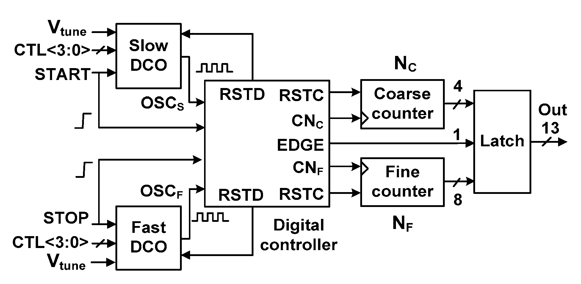
Figure 2 shows a block diagram of the proposed TDC. It consists of two DCOs, a digital controller, a coarse and a fine counter, and an output latch. The fast and slow DCOs generate outputs OSCS and OSCF, respectively. The DCOs use dual control for fine frequency tuning, which is achieved by using digital control word CTL<3:0> and tuning voltage, Vtune. The coarse and fine counter clock signals, CNC and CNF, increment the count value during coarse and fine steps, respectively. An RSTD signal is used to reset the DCOs while the two counters are reset by the RSTC signal. In the cyclic Vernier structure, the fast DCO catches up with the slow DCO, resulting in edge alignment. The EDGE signal is used to distinguish two kinds (rising/rising and rising/falling) of the edge alignment. Using a 1-bit EDGE signal, 4-bit coarse counters and 8-bit fine counters, the TDC generates a 13-bit output.
The TDC measures Tinput between the rising edges of the START and STOP signals. The START signal enables the slow DCO that has a period of TS, and the coarse counter records the number of oscillation cycles, NC, in the coarse step. Then, the coarse time, Tcoarse, is obtained by multiplying NC with TS. After a time delay of Tinput, the STOP signal arrives. It disables the coarse counter and enables the fast DCO that has a period of TF. The fine time Tfine, which is less than TS, is measured by counting the number of cycles in the fine step, NF. Because TS is slightly larger than TF, the time difference between the rising edges of the two DCOs is reduced by an amount τ = (TS − TF) in every cycle. Here, τ is the resolution of the TDC. Then, Tinput can be expressed as
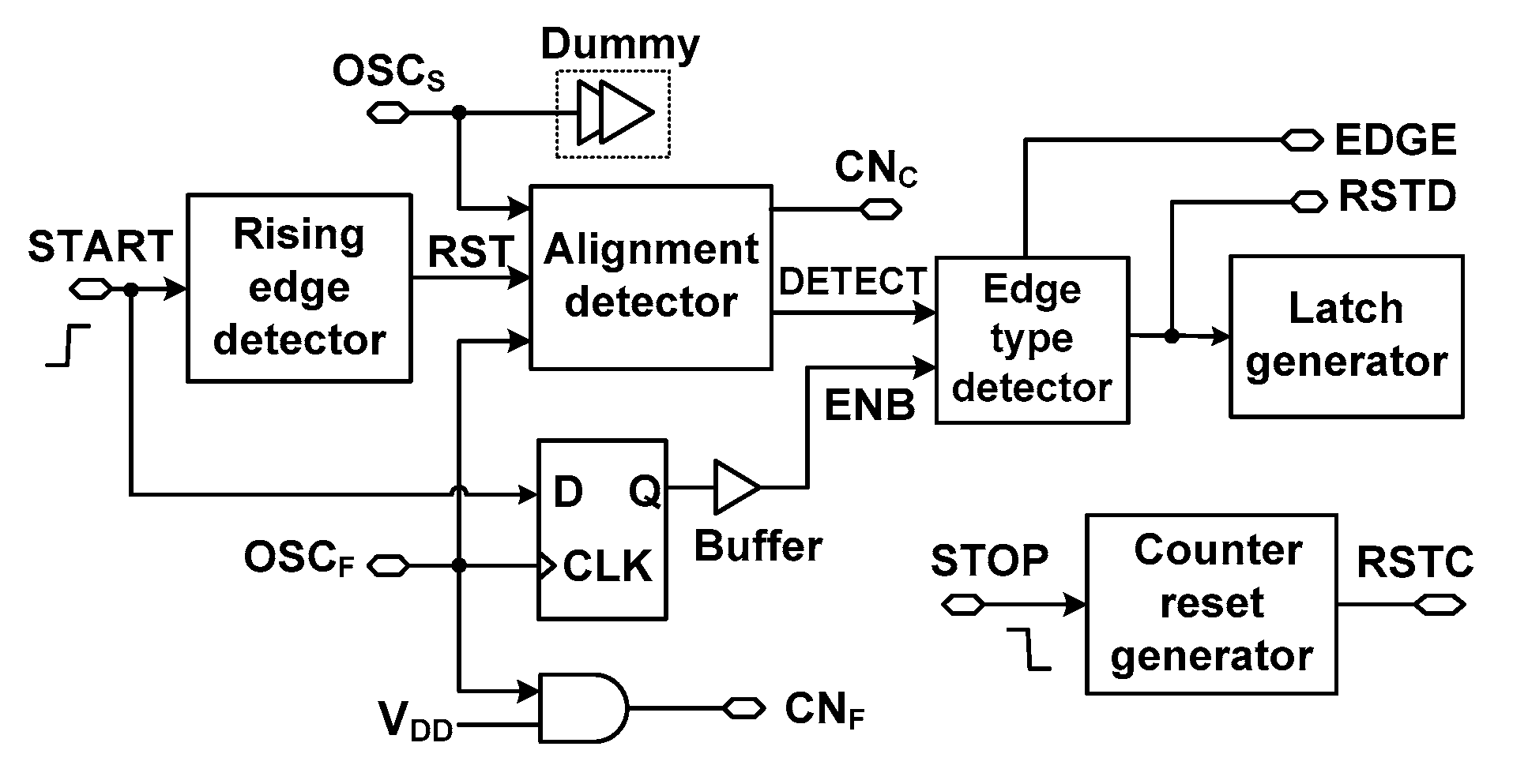
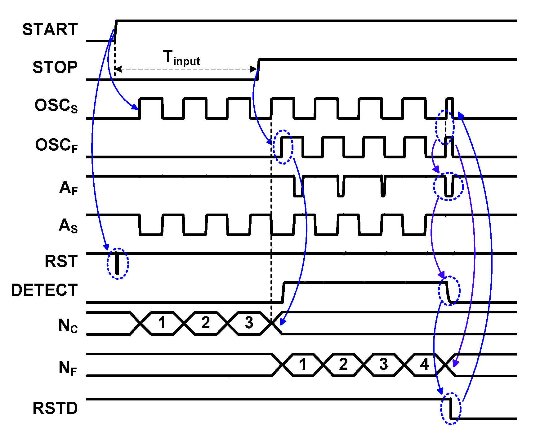
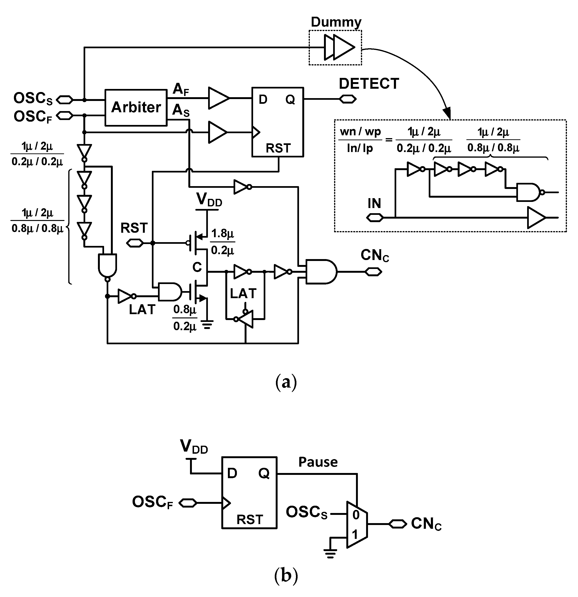
To measure Tinput, the digital controller shown in Figure 3 generates a number of control signals. The controller includes a rising-edge detector, an alignment detector, an edge-type detector, a latch generator, and a counter reset generator. A brief description of these blocks is illustrated using the timing waveform shown in Figure 4. When the rising-edge detector is activated by the START signal, it generates a global reset, RST. Using the output of OSCS, the CNC signal generated through the alignment detector increases NC. When the STOP signal arrives, it enables the fast DCO, which ends the coarse step. At this time, the alignment detector stops CNC signal, and CNF signal is generated by buffering OSCF signal through a AND gate driven by a high voltage level VDD (supply voltage), increasing NF. The STOP signal is also input to the counter reset generator for the RSTC signal, which is produced at the falling edge of the STOP signal. During the fine step, the phase of OSCF eventually catches up to the phase of OSCS. The arbiter inside the alignment detector generates outputs AS and AF. It captures the moment when the edges of OSCS and OSCF are aligned. At the moment of alignment, the DETECT signal from the alignment detector goes from high to low. Using the DETECT signal, the edge-type detector generates the RSTD signal, which stops the DCOs for power saving, and disables the CNF signal. When the conversion is finished, the edge-type detector triggers the latch generator which stores the result in the coarse and fine counters.
A Startup Time Cancellation
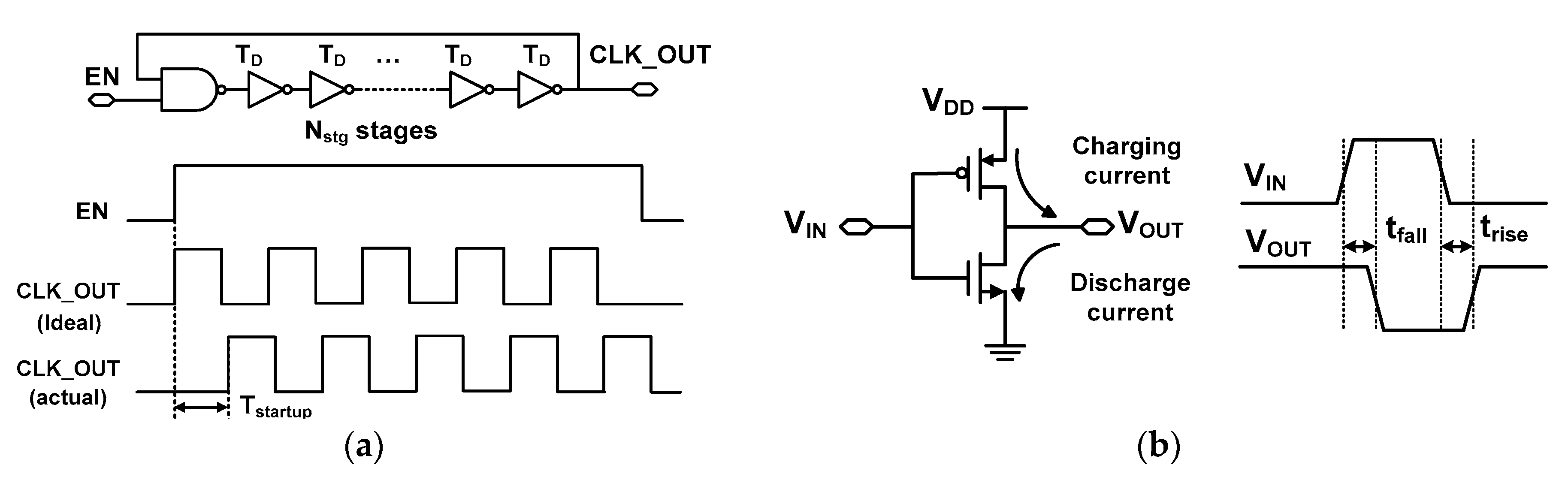
Consider a ring oscillator having an odd number of inverter stages, Nstg, as shown in Figure 5a. Ideally, when an enable signal EN is asserted, the oscillator would immediately generate the output CLK_OUT. In practice, each stage of the oscillator must accumulate some delay before producing an output. The propagation delay leads to startup time Tstartup. Assuming equal charging and discharging currents as shown in Figure 5b, the rise and fall times are approximately equal to TD as trise tfall TD, where TD is the average propagation delay of the inverter.
Assuming that each of the stages has the same characteristics, the cycle time (or period, Tcycle) of the oscillator, which is the time it takes for the output to repeat its phase, can be expressed [29] as
In the ring oscillator, Tstartup is the signal propagation time after the EN signal is enabled. Neglecting delay in the logic gate, it can be expressed as the sum of delays as
Tstartup is affected by various factors such as clock jitter, supply noise, and PVT variation. Nevertheless, Equation (4) shows that Tstartup is relatively large, on the order of Tcycle. For example, the slow DCO in this study runs at 43.1 MHz with TS = 23.2 ns. In this case, Tstartup Tcycle/2 is 11.6 ns.
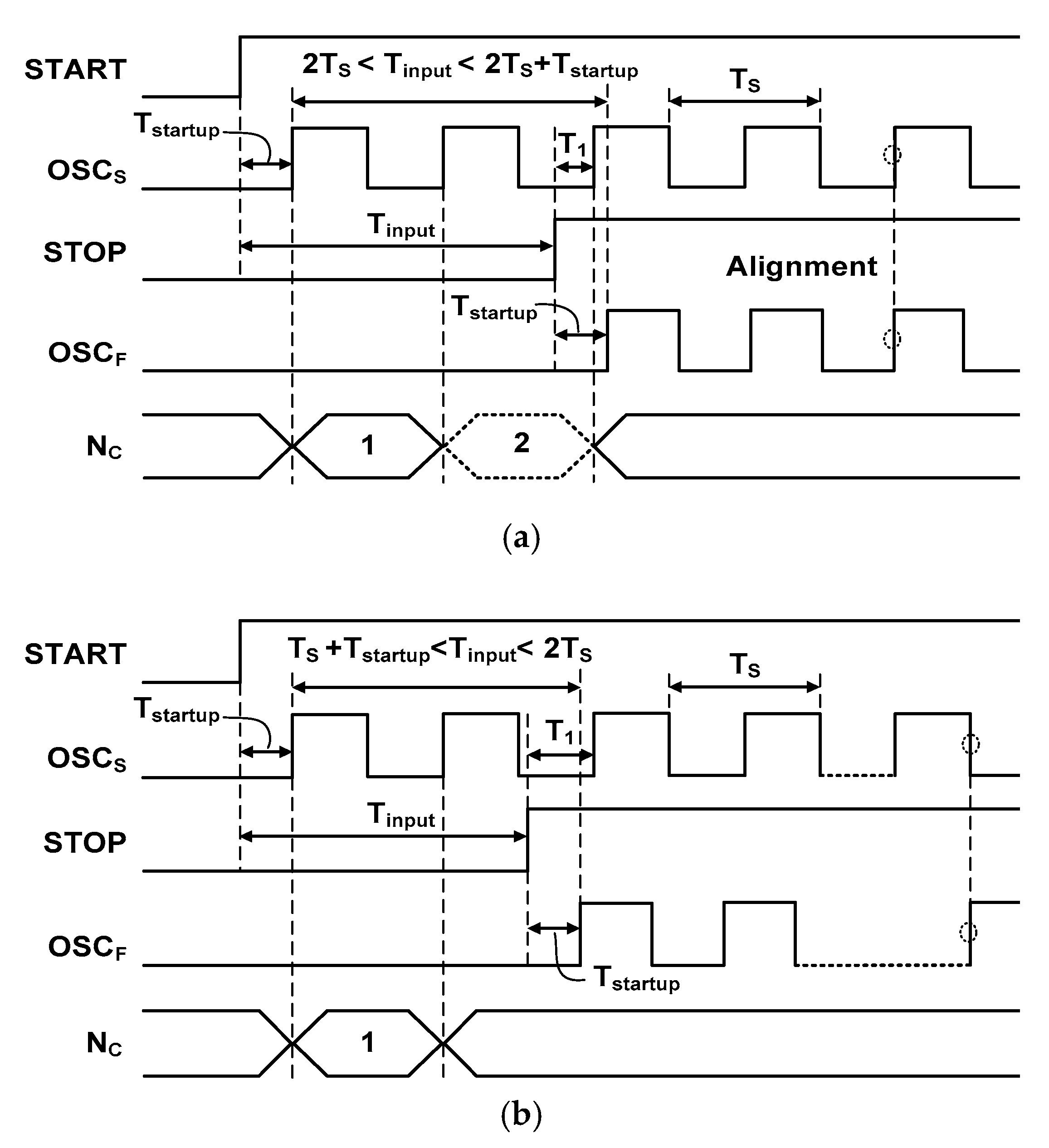
To investigate the effect of Tstartup on the linearity of the TDC, we consider the waveform as shown in Figure 6. It shows two cases for a relatively large Tstartup Tcycle/2. Here, we consider the period of coarse step with Tcycle = TS. Figure 6a shows the case when Tinput is in the range of k × TS < Tinput < k × TS + Tstartup (k = 2 in this case). When the START signal initializes the counter, the cycle of the OSCS is counted until the STOP signal disables the counter. In the case shown in Figure 6a, the counter generates an incorrect output of (k − 1) while the correct value is k. This error occurs because T1 (between the rising edge of STOP and the 3rd cycle of OSCS) is less than Tstartup. This error can be explained more generally as follows: after the START signal, the counter has to wait an amount of Tstartup to measure an oscillation cycle. However, when the STOP is activated, the counting is immediately disabled. This error cannot be simply corrected by adding one to the coarse value because there is another case. Figure 6b shows the case of j × TS + Tstartup < Tinput < (j + 1) × TS (j = 1 in this case). When the oscillation cycle is counted between the START and STOP signals, it generates the correct value of j. This case of correct counting occurs as long as Tstartup is less than T1.
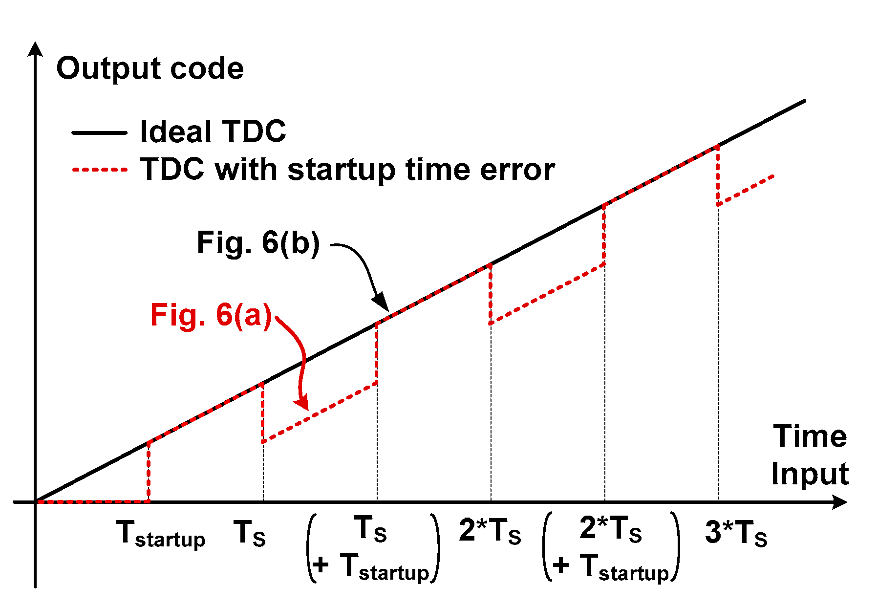
Figure 7 shows the effect of Tstartup on the transfer characteristic of the TDC. The error occurs in the region corresponding to the case of Figure 6a. The result shows that the output is periodically disturbed by the error. In the case when the STOP signal is used directly to stop OSCF, we note that the TDC does not generate the output when Tinput < Tstartup. This is because OSCS is not yet started and the STOP signal has already arrived. Therefore, there are none of any oscillations initiated in the two DCOs. The Tstartup affects only the coarse step and generates the coarse counting error. Therefore, the influence of Tstartup can be ignored when Tinput is small, for example, the error does not occur for the case of Tstartup < Tinput < TS as shown in Figure 7. When Tinput is small, the TDC skips the coarse step and operates only in the fine step. Although OSCF is delayed by Tstartup, we note that a similar delay occurs in the OSCS. In this work, we extract Tinput from the first incoming edges between OSCS and OSCF. Therefore, Tstartup does not generate an error in the fine step. In the case when Tinput is in a small range, for example, 2TS < Tinput < 2TS + Tstartup as shown in Figure 6a, the coarse error can be considered as an offset which can be removed by post-processing. When Tinput is large, however, the error cannot be considered as an offset. Because the range of the Tinput is unknown prior to the measurement, calibration of this nonlinearity is rather complicated.
The above result indicates that the effect of Tstartup on the TDC’s linearity may be mitigated by reducing Tstartup. By modifying the logic gate where the EN signal is applied, we can indeed reduce Tstartup; when the logic gate for the EN signal in Figure 5a is moved to the last stage of the oscillator, it can be shown that Tstartup is inversely proportional to Nstg as Tstartup Tcycle/(2Nstg) [29]. By increasing Nstg, Tstartup can be reduced; this is achieved with increased power, accumulated jitter, and low speed (Tcycle 2NstgTD).
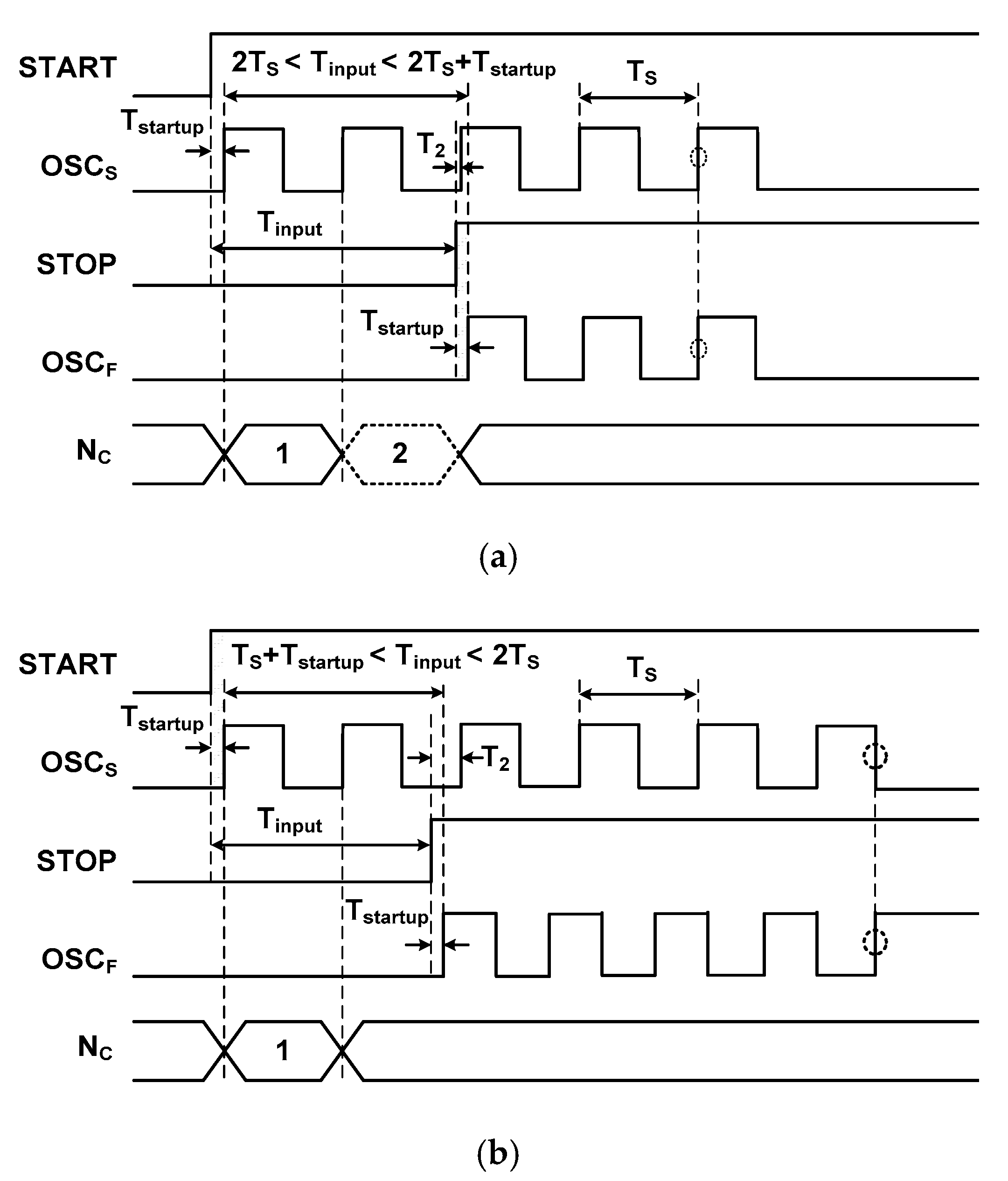
Figure 8 shows two cases of waveforms for a relatively small Tstartup. The result is shown for Tstartup TS/(2Nstg) with Nstg = 5. Figure 8a shows the case of k × TS < Tinput < k × TS + Tstartup (k = 2 in this case). Here, the STOP signal is activated before the 2nd cycle of OSCS is finished and the counted value is (k − 1), which is incorrect. The error is generated because T2 (the time between STOP and the rising edge of 3rd OSCS) is smaller than Tstartup, and OSCS is delayed by Tstartup. Figure 8b shows a case in which the STOP signal is activated before the 2nd cycle of OSCS is finished, which counts the correct value. In this case, T2 is larger than Tstartup, and the small Tstartup time does not affect the counting result. These results are similar to those shown in Figure 7, except for the reduced width of the error region, showing that even when Tstartup is reduced, incorrect counting still occurs in some cases. Therefore, the output is necessarily disturbed by a constant offset in the transfer characteristic.
The counting error caused by Tstartup is related to the method used to detect the moment when the coarse step ends. In the actual TDC, the START signal for the coarse step is delayed by an amount of Tstartup. In the case when the STOP signal is used to disable the coarse step, there is no compensation for the delay caused by Tstartup. Therefore, the conventional approach of using the STOP signal to end the coarse step can generate the counting error. In summary, this method generates an error because OSCS is used to directly clock the counter.
To achieve good linearity over a wide input range, we propose a startup time correction technique. The proposed technique is based on the idea of using two DCOs with matched Tstartup. In this system, Tinput is equal to the time difference between OSCS and OSCF instead of between the START and STOP signals. In more specifically, CNC is generated from OSCS. Before OSCF is activated in the coarse step, the number of OSCS cycles is counted to generate NC. When OSCF is activated in the fine step, it controls the latch to stop generating NC. In this way, NC is generated indirectly from OSCS, not from the delayed rising edge of OSCS. The proposed solution is implemented using the alignment detector as explained in the next section.
B. Alignment Detector and Arbiter
Figure 9a shows the schematic of the alignment detector. It performs two critical tasks: (1) detecting the edge alignment of two DCOs and (2) controlling the counter timing for startup time correction (explained above). When the conversion is started, an active-low reset signal RST changes the charging node ‘C’ to high and enables the logic gate that follows. In the coarse step, OSCS is enabled. The arbiter receives the OSCS signal and its output AS goes through another inverter to generate CNC. The CNC signal is a delayed and gated version of OSCS, which is used to increment the coarse counter. It is generated through the arbiter to immediately stop the counting when the edge alignment occurs. During the coarse step, OSCF is inactive and the latch control signal LAT is low at this time. Thanks to the cross-coupled inverters used for the latch, the node ‘C’ is kept at a high level during the coarse step. The reason why we use the latch is to make sure that the NAND logic used for gating the CNC is enabled even node ‘C’ is being discharged by leakage current.
The coarse step is finished when OSCF is activated. It generates a short pulse for the LAT signal, which pulls down the node ‘C’ and disables the logic gate for CNC. And the TDC enters the fine step. In the fine step, OSCF catches OSCS after some number of cycles. The alignment moment is detected by an arbiter followed by a D flip-flop (D-F/F), which generates the DETECT signal. The latch is added because the output of the arbiter is level sensitive.
We note that the activation and de-activation of CNC are performed by the two DCOs having closely matched Tstartup; the time between START and OSCS is closely matched to the one between STOP and OSCF. By using OSCF to control CNC, the delay of Tstartup does not cause an error in the coarse counter. In comparison, the conventional approach using the STOP signal for counter control does not consider Tstartup and can result in incorrect counting as shown in Figure 7.
We may consider using OSCS as the coarse counting clock and utilizing the first rising edge of OSCF to directly stop the coarse counting. This approach looks intuitive, however, it can create unbalanced load in the OSCS and OSCF paths. In addition, the implementation of the counter control signal for CNC requires a pause function instead of a simple reset. When OSCF arrives, it should stop the coarse counter to end the coarse step. At this time, we note that its counted value should be preserved for TDC’s output. This is because OSCS still operates during the fine step until coincidence with OSCF is detected. One example circuit realizing the pause function is shown in Figure 9b. This approach has the advantage of simple logic and generates a small delay in stopping the CNC signal. Because of the setup time of the D-F/F, however, this approach may generate an unexpected counting error. This is in particular problematic when Tinput is close to an integer multiple of OSCS period. Another issue of using the simple logic is that the information available from the output AS of the arbiter is wasted; it can be used to stop the coarse counting without causing additional loading to the DCOs.
To achieve the proposed startup time correction, a good balance between the two outputs of the DCO is necessary. The arbiter itself has an inherently symmetric structure (see Figure 10). Therefore, we consider balanced loading at the two inputs of the arbiter. If the loading at the two ports is different, there can be a mismatch in the transient time of the two DCOs, which increases the probability of incorrectly detecting alignment. To achieve balanced loading, we insert a dummy at the output of OSCS. The size of the dummy is determined by performing extensive Monte-Carlo simulations that consider both local and global process variation. In this way, we are able to mitigate the load mismatch at the two outputs of OSCS and OSCF. The upper limit to the estimated value of Tstartup is Tcycle/2 as indicated by Equation (4). In the case when the startup times of OSCS, (Tstartup,S) and OSCF (Tstartup,F) are not equal, the difference can be approximated to half the resolution τ as
Fortunately, the difference is an offset error with a mean value of τ/2, which can be easily removed by post-processing. We consider this post-processing because there can exist the mismatch caused by environmental noise and random jitter even when Tstartup has been matched well in the simulated conditions.
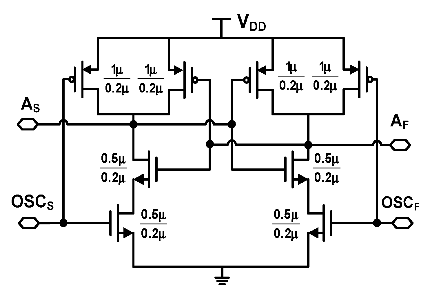
Figure 10 shows the schematic of the arbiter. The arbiter is adapted from the previous work [6], and modified to reuse current for increasing the transconductance and speed. Similar to the arbiter [6], which keeps the output in good balance during the reset phase, the output of the proposed arbiter is also reset when both inputs are high. Circuit simulations show that the average current of the proposed arbiter is 16 μA at a supply voltage VDD = 1.8 V. In comparison, the current is 53 μA for the arbiter [6], in which the high current is attributed to leakage current occurring when the two inputs are high and the outputs are in the middle. The proposed arbiter achieves a delay time from input to output of about 100 ps which is two times smaller than that of the previous work [6]. Compared with the conventional D-F/F and dynamic (true single-phase clocking-based) D-F/F, the proposed arbiter achieves better load balance. This is because the arbiter maintains a symmetric current steering path between two inputs while the D-F/F has different loads for the clock and data paths.
Although the arbiter has a symmetric structure, an offset time, toffset, occurs due to the mismatch of device parameters, routing parasitics, and unbalanced loading. When the alignment of two DCOs occurs, the edge of OSCF leads/lags that of OSCS by the time difference δ. In the case of δ > toffset, the difference between the input and the estimated value is τ − δ which is smaller than the resolution τ of the TDC. In the case of δ < toffset, the fine step counts one more cycle and the error increases to 2τ − δ. By careful symmetric layout, we reduce toffset < 2 ps, which is quite small when compared to the range of the TDC.
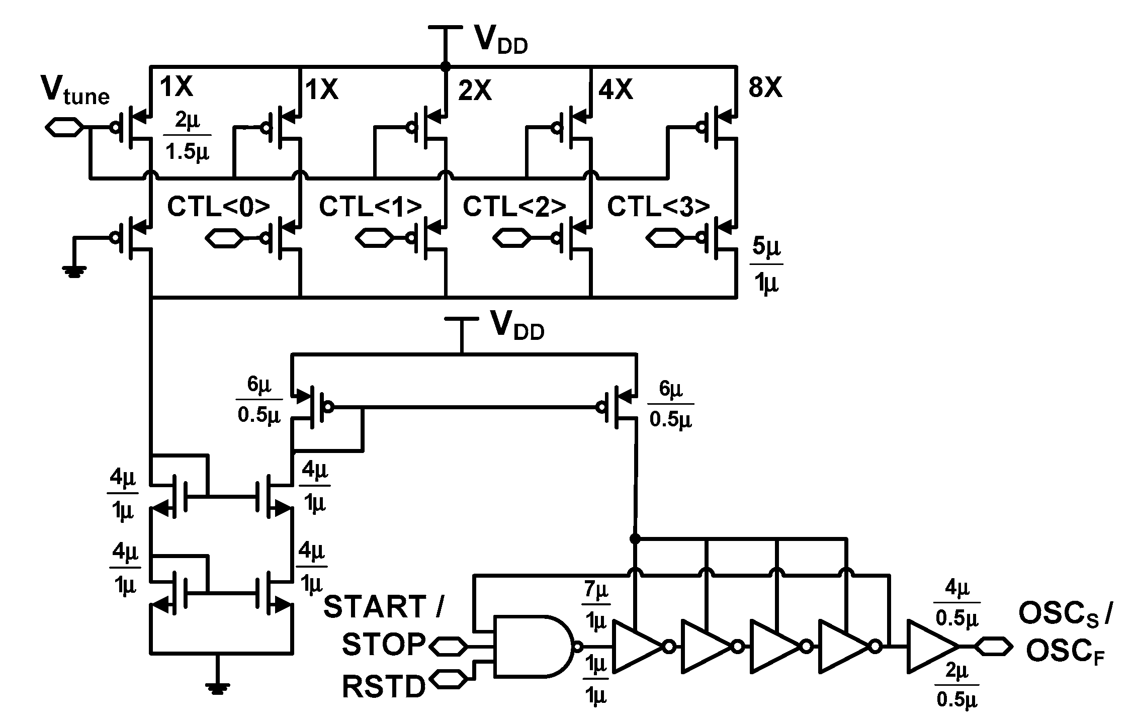
C. Digitally Controlled Oscillator
Because the resolution of the cyclic Vernier TDC is determined by the frequency difference between the two DCOs, fine frequency control is necessary. In the previous study [6], there is no frequency tuning mechanism except the gating function. Our previous work included a DCO with a single control for frequency tuning [27]. In this work, we propose a DCO with dual frequency control. Figure 11 shows the schematic of the DCO. The oscillation is enabled by START and STOP signals for the slow and fast DCOs, respectively. The layout of this system is carefully designed to enhance matching between the two DCOs; the inverter stages of two DCOs are placed in an interdigitated manner and the binary-weighted current mirrors are designed using the common-centroid layout with a dummy. The dual-frequency control is implemented using four-bit control word CTL<3:0> and a tuning voltage Vtune applied to the current mirrors globally controls the amount of the current to the DCO. The CTL<3:0> adjusts the fine current via the digital-to-analog converter that acts as the discrete frequency controller for the DCO. The frequency fDCO of the DCO can be expressed as
where TD,NAND and TD,INV is the delay of the NAND gate and the inverter, respectively. When Vtune and CTL<3:0> are applied, only TD,INV is varied while TD,NAND is kept constant. Even though TD,NAND is not controlled, it does not have much impact on the precise quantization of fDCO. This is because we are able to achieve fine-tuning of fDCO using Vtune. By varying TD,INV, the proposed dual frequency control method achieves frequency tuning in 20 kHz steps over a 4.8 MHz range.
The RSTD is a reset signal for the DCO. When the conversion is finished, it stops the DCO to reduce power consumption. After the conversion, the counter is reset as is the accumulated jitter. This observation suggests that the error can be reduced by increasing the operating frequency of the DCO. However, the high operating frequency is accompanied by increased jitter. With this tradeoff and power consumption in mind, we choose the frequency of two DCOs to be 43.1 and 43.8 MHz. This corresponds to the resolution τ = 371 ps.
D. Edge-Type Detector
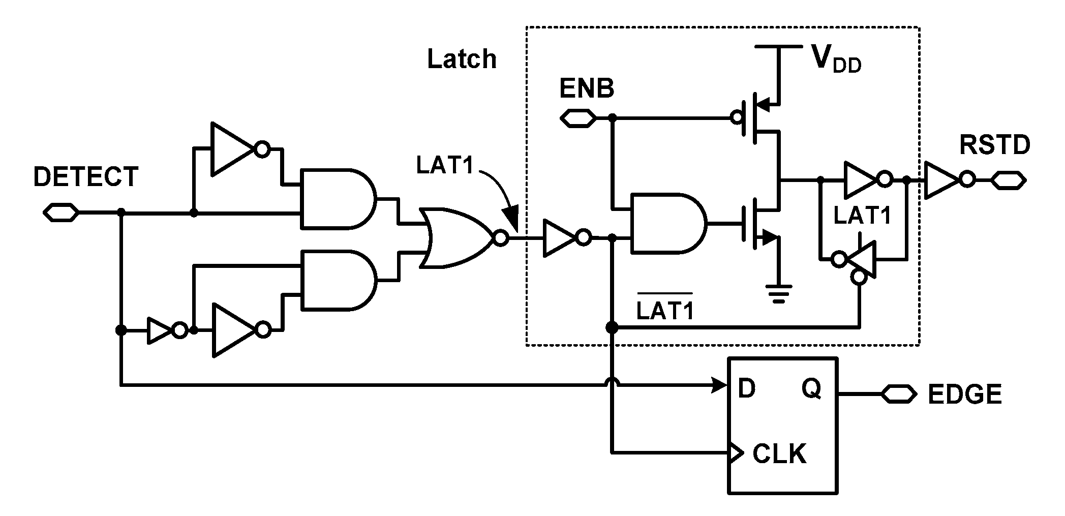
Figure 12 shows the schematic of the edge-type detector. The detector receives inputs DETECT and ENB and generates the EDGE and RSTD signals. The detector includes a D-F/F and a latch. The EDGE is generated through the D-F/F. The RSTD signal is generated through the latch which is controlled by the DETECT signal. This approach is used to ensure proper detection of edge alignment of the two DCOs. There are two transitions of DETECT signal (see Figure 4). The first transition occurs when OSCF is starting and sets the DETECT signal to high. DETECT then transitions to low when alignment occurs. To prevent detecting a false alignment, the ENB signal is used to discard the first transition of the DETECT signal.
The ENB signal is generated by the D-F/F in the digital controller (see Figure 3). Before the START signal, the low level of ENB keeps the RSTD at a high level. After the START signal, ENB is kept high. By the second transition of the DETECT signal, which indicates the end of conversion, the active-low RSTD signal is generated. This keeps the starting node of DCO high, thus freezing the oscillation, and it reduces power consumption by stopping the DCO.
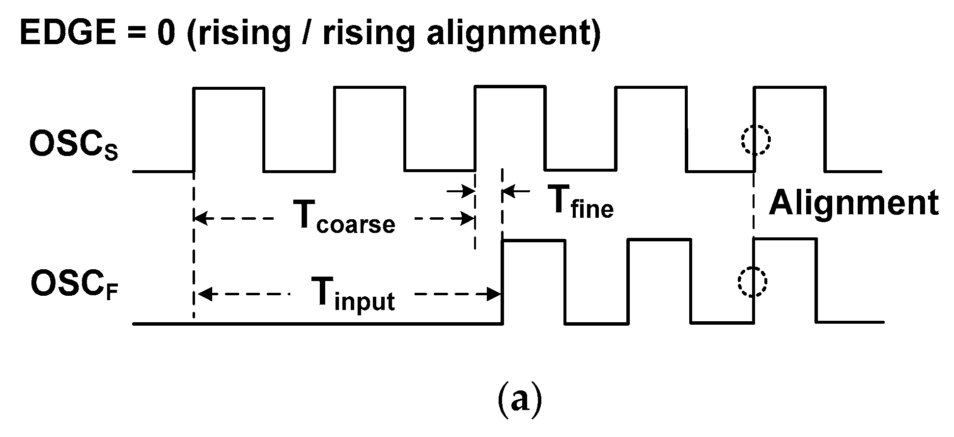
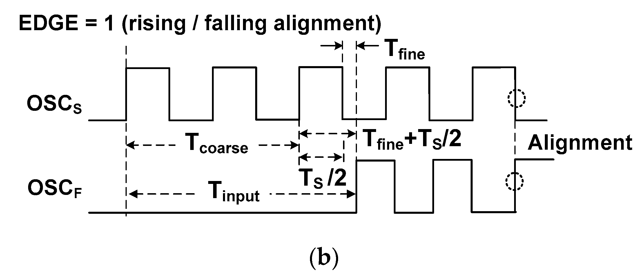
The EDGE signal indicates the type of edge alignment. In the case when both OSCS and OSCF are rising at the moment of alignment, as shown in Figure 13a, the DETECT signal goes from high to low generating EDGE = 0. This case corresponds to Tfine < TS/2. In the case of a rising/falling alignment, as shown in Figure 13b, the DETECT signal goes from low to high generating EDGE = 1. In this case, the duration of the fine step can be greater than half of a period. To handle this issue, we add TS/2 when EDGE = 1 so that the fine counter can measure a duration smaller than TS/2. In this way, the size of the fine counter is reduced by detecting both alignments. In addition, this strategy reduces power and increases conversion speed. Because of the operating sequence of the alignment detector in which OCSF stops the CNC signal (see Figure 9), CNC is activated one more time. Since this occurs in every conversion, it can be considered as an offset to NC. Accounting for the offset and the status of the EDGE signal, the estimated time input is obtained using
3. Measured Results
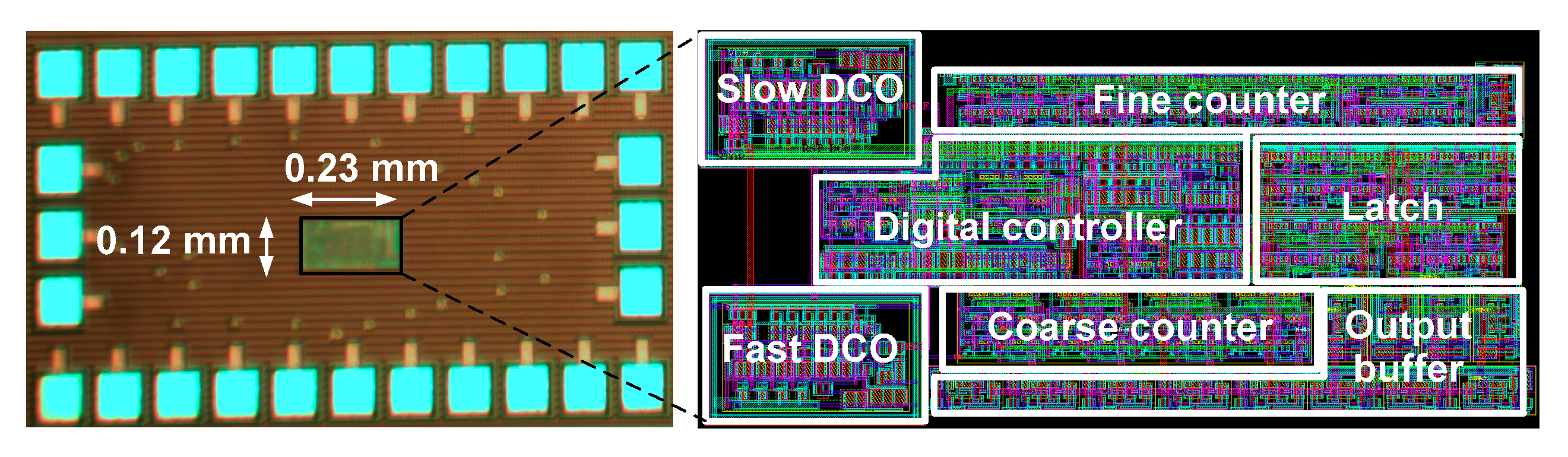
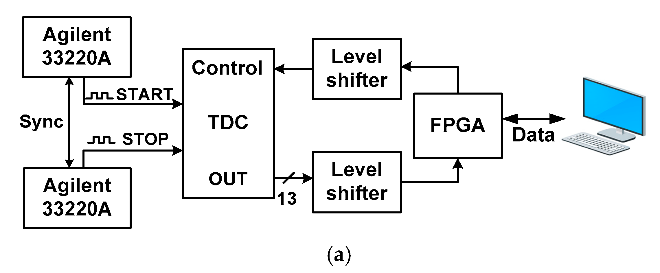
Figure 14 shows the chip microphotograph of the fabricated TDC with core layout. The size of the core is 0.028 mm2. Figure 15a shows the measurement setup for the TDC. Before characterizing the TDC, the DCOs are operated in a free-running mode to determine and calibrate the oscillation frequencies. Two function generators (Agilent 33220A) are used to create input signals (START and STOP). To reduce the number of I/O pads, a parallel to serial converter is included in the chip. An field-programmable gate array (FPGA) board is used to collect and convert the serial output to 13-bit data. Two level shifters are used to interface between the FPGA and the TDC. Finally, the data is transferred to a computer for further processing.
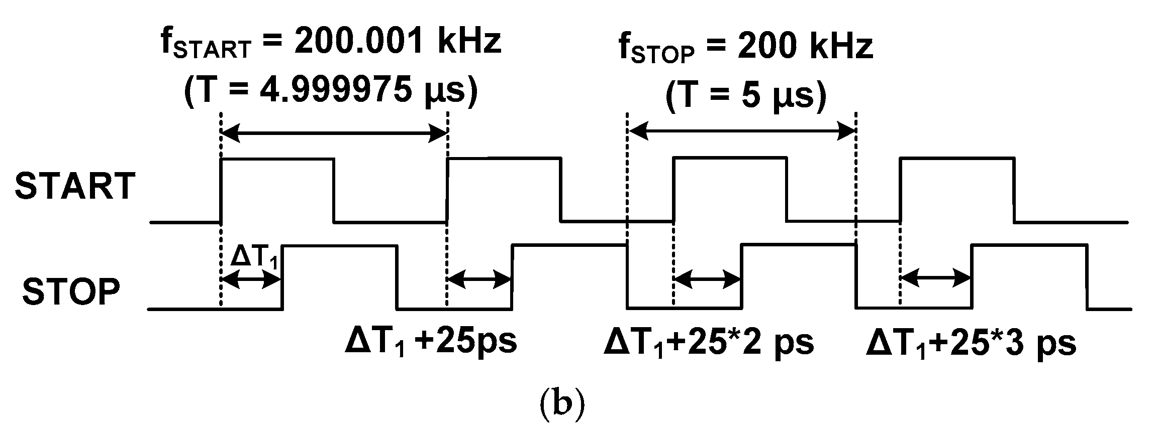
Characterizing the TDC is challenging, especially under the time sweep condition, because it requires precise control of time differences over a relatively long period. In this work, we use function generators to provide the START and STOP signals with slightly different frequencies. When the two signals are synchronized with a 1 Hz frequency difference, this method allows for increasing Tinput in steps of 25 ps, as shown in Figure 15b. Thanks to the synchronization feature of the instrument, we precisely configure the time difference between two signals with a standard deviation of about 200 ps. Because the jitter from the equipment does not allow ideal time step, it does affect the test results. To handle this issue, we perform a number of measurements and take the average. In this way, the error caused by the jitter from the equipment can be averaged out. When combined with nonlinearity caused by mismatch, the linearity is further affected because more variation is added. Even with this nonlinearity, our measured result shows that the TDC achieves a relatively good linearity using the proposed approach (see Table 1).
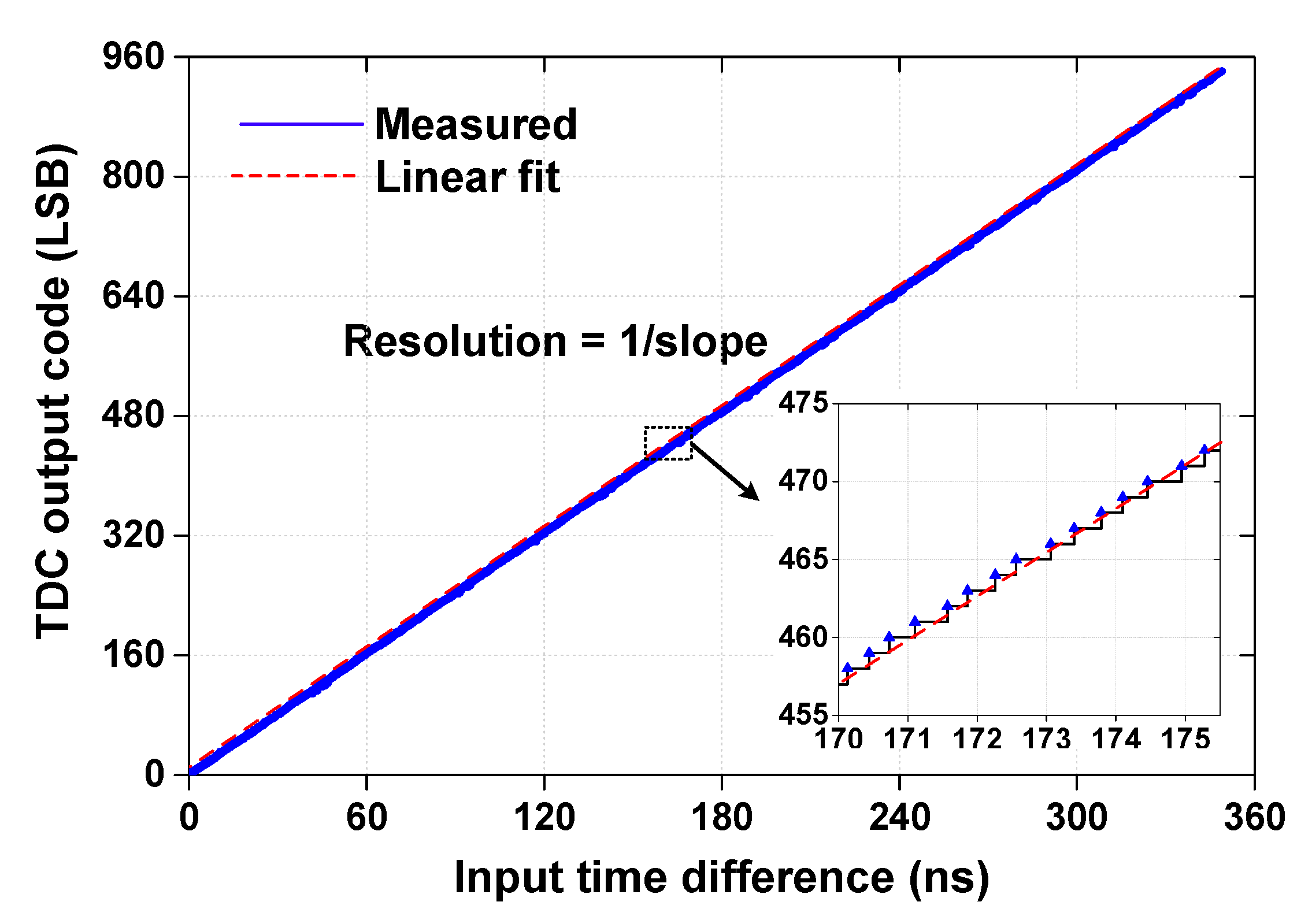
Figure 16 shows the measured transfer characteristic of the TDC obtained by taking an average of eight measurements. Each measurement includes 14,400 steps with 25 ps increment. The result shows a relatively large input range of 355 ns. The maximum coarse and fine times of the proposed TDC are and respectively. The ‘−1’ term is used to correct the offset in the coarse clock; CNC is activated one more time before OSCF stops CNC signal. The ‘+0.5’ term is added in consideration of the EDGE bit. The calculated result obtained using this expression is 371 ns which agree with the measured range. The inset of Figure 16 shows a magnified view of a portion of the curve. The resolution of a TDC is defined as the minimum time interval that a TDC can resolve [30], and it can be estimated as the reciprocal of the slope [6]. From the linear fitting curve of the data in Figure 16, we obtain a resolution of 377 ps, which agrees with the calculated resolution of 371 ps. The relatively low resolution is limited by the frequency difference of the two DCOs, which operate at a low speed for small power consumption; the result is still suitable for a long-range TOF application. When the result is used for range sensing, it corresponds to a detection range of 53.2 m and a resolution of 5.65 cm.
System level simulations of the TDC show that the power consumption depends on Tinput; a longer fine step requires extended DCO oscillation time before the alignment event occurs, thus, consuming more power. When we take an average value for the maximum Tinput = 355 ns, the TDC consumes 0.65 mW which is a total power (active and standby power). The latency also depends on the Tinput; it increases with each extended coarse cycle of Tinput. When the maximum range is covered, it requires the longest conversion time and in this case, the conversion rate is 0.67 MS/s.
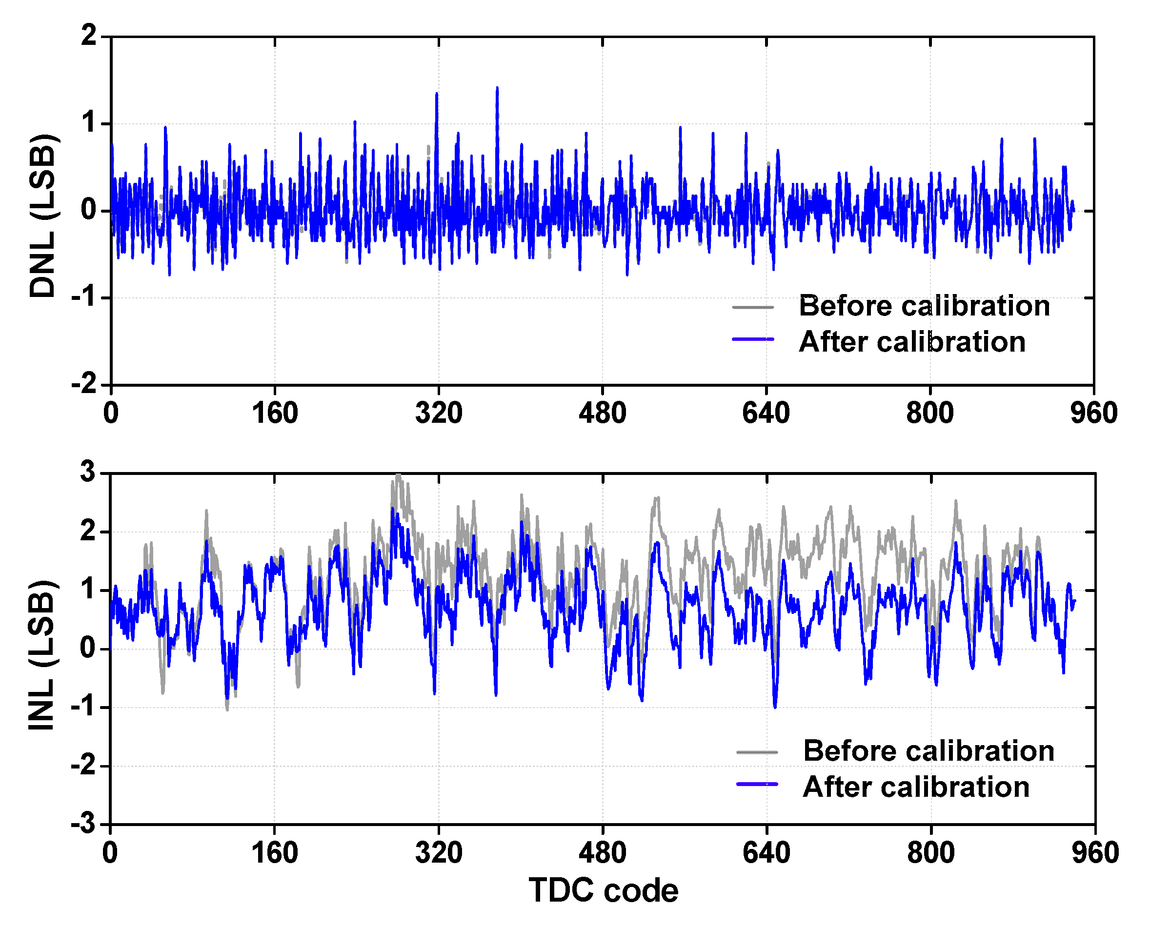
We obtain DNL and INL using code density method [6]. The size of the bin is 15 and the maximum code is 941 LSB. Figure 17 shows the result before and after calibration. The calibration is required because the static test is swept over a relatively long Tinput and the input signals can be corrupted by the jitter from the equipment. To deal with this issue, we perform calibration by removing incorrect codes by checking consistency with the previous and subsequent codes. Using this method, we calibrate out 349 codes (2.4%) which are out of range (3-sigma) among the 14,400 codes. We note that this calibration is not needed for single-shot measurement. After calibration, the TDC achieves a DNL of 1.41 LSB (maximum) and 0.28 LSBrms. The INL performance is 2.31 LSB (maximum) and 0.96 LSBrms. Before calibration, we obtain a DNL of 0.31 LSBrms and an INL of 1.41 LSBrms. When the INL is used to estimate the discrepancy between the estimated and real distance, the result corresponds to an error of 5.42 cm.
In cyclic TDCs based on an oscillator, nonlinearity occurs due to layout mismatch, supply noise, signal cross-talk, and PVT variation. Compared to other studies (see Table 1), the proposed TDC achieves good linearity. We note that the shape of INL is changed periodically. This is attributed to the accumulated nonlinearity in the coarse step. Using the measured data, we obtain the number of bits NBit = log2 (maximum input range/resolution) to be 9.88 bits. Taking nonlinearity into consideration, we obtain the equivalent number of linear bits Nlinear = NBit − log2(INL + 1) to be 8.15 bits [23].
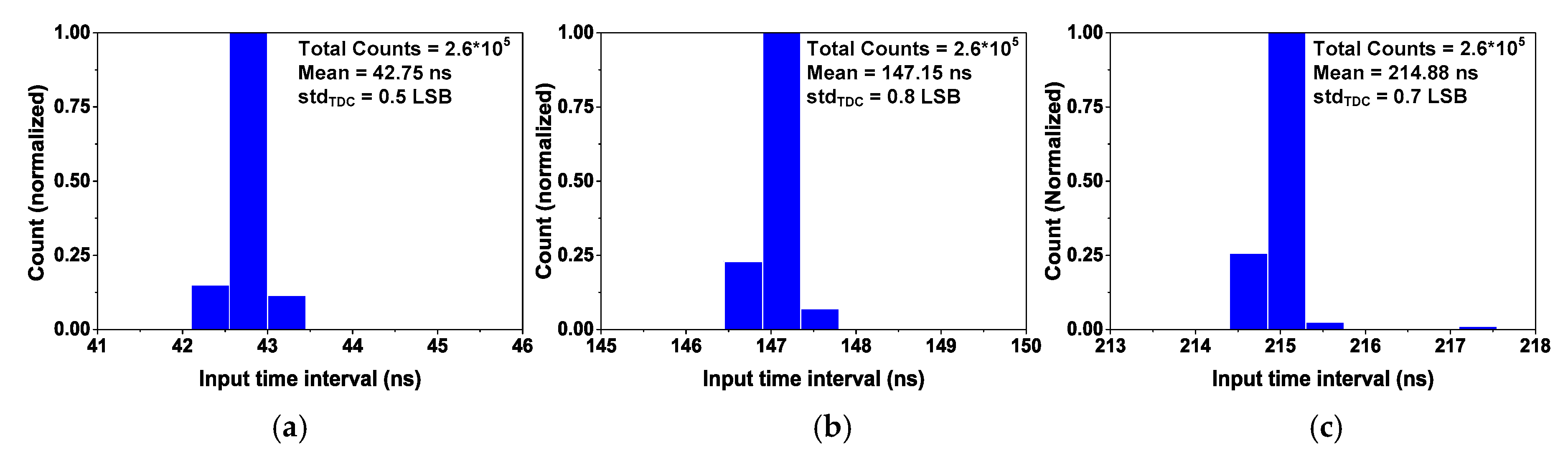
The precision of the TDC is evaluated using the single-shot measurement. Figure 18 shows the result for three cases of Tinput. In each measurement, we keep the same Tinput and repeat the conversion up to 260,000 times, which is large enough to observe the precision of the TDC. The result shows a standard deviation, stdTDC, of 0.5, 0.8, and 0.7 LSB for Tinput = 41.2, 148.3, and 217.7 ns, respectively. The results agree with our expectation that stdTDC increases with Tinput due to accumulated jitter.
Table 1 shows the performance comparison with other studies. The work in [5] integrates TDCs for single-photon avalanche diode array to perform time-correlated single-photon counting. By using an external delay-locked loop (DLL), this work reduces the circuit complexity; the drawback is relatively poor linearity. The work in [6] presents a gated-Vernier oscillator that achieves a resolution of 7.3 ps with a relatively small input range of 9 ns. Using a look-up table for correcting the INL error, this work achieves a DNL of 0.8 LSBrms and an INL of 1.2 LSBrms. The work in [13] presents a detailed analysis of compensating PVT variations for the TDCs. By using a global compensation loop based on a phase-locked loop (PLL), the TDC in this work achieves an input range of 716 ns with a resolution of 357 ps. The work in [21] realizes a cyclic TDC using a hardware description language (HDL) which allows chip synthesis with automatic place-and-route tools. The work in [23] presents a two-step TDC based on a pseudo-differential TVC and a 6-bit SAR ADC. This work achieves a high conversion rate of 120 MS/s with a power of 3.73 mW. These works achieve a high resolution of 5.5 ps [21] and 0.63 ps [23]. However, the input range is 4.5 ns and 0.3 ns, which is not sufficient for TOF applications that demand wide ranges. Another work in [31] presents per-pixel TDC for PET imaging. The result achieves a resolution of 64.5 ps with an input range of 50 ns, however, its relatively poor linearity (max INL = 3.9 LSB) needs further correction. Thus, this work can suffer from a large error when applied to a TOF range sensor. The work in [32] presents detailed circuit techniques for all digital TDC to achieve a high resolution of 10 ps, however, only a limited amount of measured data is available. Two works developed for TOF imager, which realizes the TDC using a ring oscillator and a ripple counter, present TDCs achieving a high input range [13,33]. By locking phase and frequency among the ring oscillators, the TDC in [33] achieves an input range of 2 μs with a resolution of 125 ps. With a simple structure, it is suitable for realizing in-pixel TDCs for dTOF image sensors; compared to our work, the linearity performance (max INL = LSB) needs further improvement.
The results in Table 1 show that it is challenging to achieve both high dynamic range and high resolution with a good linearity. Those TDCs that target PLL applications achieve a high resolution with a good figure-of-merit (FOM), however, provide only a limited input range [21,23]. The systems developed for TOF applications provide an increased input range [5,32], but show relatively poor linearity. References [21,23] achieve better FOM than ours, but these works are realized using the 65 nm process for a small input range of 4.5 and 0.3 ns, respectively. Obviously, the range is not suitable for TOF applications requiring a high input range. Except for [13,33], which are realized using a simple ring oscillator and a ripple counter, our work achieves the lowest power consumption. In the cyclic TDC, a large part of power is consumed by DCOs. Therefore, we carefully design the DCOs for low power: (1) we use the RSTD signal to stop the DCO when the conversion is done; (2) we use a small number of five ring stages; (3) we operate the DCOs in low speed although this approach trades the resolution for power. Overall, our TDC in this work achieves a relatively high input range of 355 ns with a good linearity and a low power.
The number of bits NBit can be used to quantify the dynamic range by considering input range and the resolution. A better metric is Nlinear which takes the linearity performance into account. Compared to other work [23,31], our work achieves an Nlinear of 8.15 which indicates good linearity. Increasing performance by 1-bit in an ADC with more than 12-bit resolution is challenging when both area and linearity is constrained. Even though the TDC in this study doesn’t use a capacitor as do SAR ADC, the area and circuit complexity increase in a similar manner. Therefore, a TDC achieving both high dynamic range and resolution tends to be costly and power-hungry, which will be challenging to realize in portable applications. The proposed TDC is suitable for low-power TOF sensor applications demanding both a high input range and a good linearity.
4. Conclusions
In this paper, a low-power cyclic Vernier two-step TDC having a high input range has been designed, fabricated, and successfully characterized. The high input range is achieved by addressing the nonlinearity caused by the startup time in the conventional cyclic TDC. We solve this problem successfully by using DCOs with matched startup times and a high-precision alignment detector. The alignment detector performs precise detection of edge alignment of the two DCOs and controls the counters with proper timing to compensate for the delay caused by the startup time. The proposed TDC achieves a high input range up to 355 ns and a resolution of 377 ps while consuming an average power of 0.65 mW. The proposed TDC can find a useful application in various TOF applications such as TOF ranging and biomedical imaging.
Author Contributions
V.N.N. designed the TDC, performed the experimental work, and wrote the manuscript. D.N.D. performed circuit simulations and edited the manuscript. Y.C. gave comment to the paper and revised the manuscript. J.-W.L. conceived the project, organized the paper content, and edited the manuscript.
Funding
This research was supported by the Basic Science Research Program through the National Research Foundation of Korea (NRF-2018R1A2A2A05018621).
Acknowledgments
The chip fabrication and CAD tools were made available through the IDEC (IC Design Education Center).
Conflicts of Interest
The authors declare no conflict of interest.
References
- Zhang, M.; Wang, H.; Liu, Y. A 7.4 ps FPGA-based TDC with a 1024-unit measurement matrix. Sensors 2017, 17, 865. [Google Scholar] [CrossRef] [PubMed]
- Perenzoni, M.; Perenzoni, D.; Stoppa, D. A 64 × 64-Pixels digital silicon photomultiplier direct TOF sensor with 100-MPhotons/s/pixel background rejection and imaging/altimeter mode with 0.14% precision up to 6 km for spacecraft navigation and landing. IEEE J. Solid-State Circuits 2017, 52, 151–160. [Google Scholar] [CrossRef]
- Tanveer, M.; Nissinen, I.; Nissinen, J.; Kostamovaara, J.; Borg, J.; Johansson, J. Time-to-digital converter based on analog time expansion for the 3D time of flight cameras. In Proceedings of the Image Sensors and Imaging Systems 2014, San Francisco, CA, USA, 2–6 February 2014. [Google Scholar]
- Min, S.D.; Kim, J.K.; Shin, H.S.; Yun, Y.H.; Lee, C.K.; Lee, M. Noncontact respiration rate measurement system using an ultrasonic proximity sensor. IEEE Sens. J. 2010, 11, 1732–1739. [Google Scholar]
- Field, R.M.; Realov, S.; Shepard, K.L. A 100 fps, time-correlated single-photon-counting-based fluorescence-lifetime imager in 130 nm CMOS. IEEE J. Solid-State Circuits 2014, 49, 867–880. [Google Scholar] [CrossRef]
- Cheng, Z.; Deen, M.J.; Peng, H. A low-power gateable Vernier ring oscillator time-to-digital converter for biomedical imaging applications. IEEE Trans. Biomed. Circuits Syst. 2016, 10, 445–454. [Google Scholar] [CrossRef] [PubMed]
- Paschalidis, N.; Stamatopoulos, N.; Karadamoglou, K.; Kottaras, G.; Paschalidis, V.; Sarris, E.; McNutt, R.; Mitchell, D.; McEntire, R. A CMOS time-of-flight system-on-a-chip for spacecraft instruments. IEEE Trans. Nucl. Sci. 2002, 49, 1156–1163. [Google Scholar] [CrossRef]
- Gariepy, G.; Tonolini, F.; Henderson, R.; Leach, J.; Faccio, D. Detection and tracking of moving objects hidden from view. Nat. Photonics 2016, 10, 23–26. [Google Scholar] [CrossRef] [Green Version]
- Poland, S.P.; Krstajić, N.; Monypenny, J.; Coelho, S.; Tyndall, D.; Walker, R.J.; Devauges, V.; Richardson, J.; Dutton, N.; Barber, P.; et al. A high speed multifocal multiphoton fluorescence lifetime imaging microscope for live-cell FRET imaging. Biomed. Opt. Express 2015, 6, 277–296. [Google Scholar] [CrossRef] [PubMed]
- O’Toole, M.; Lindell, D.B.; Wetzstein, G. Confocal non-line-of-sight imaging based on the light-cone transform. Nature 2018, 555, 338–341. [Google Scholar] [CrossRef] [PubMed]
- Shin, D.; Xu, F.; Venkatraman, D.; Lussana, R.; Villa, F.; Zappa, F.; Goyal, V.K.; Wong, F.N.C.; Shapiro, J.H. Photon-efficient imaging with a single-photon camera. Nat. Commun. 2016, 7, 12046. [Google Scholar] [CrossRef] [PubMed] [Green Version]
- Ren, X.; Connolly, P.W.R.; Halimi, A.; Altmann, Y.; McLaughlin, S.; Gyongy, I.; Henderson, R.K.; Buller, G.S. High-resolution depth profiling using a range-gated CMOS SPAD quanta image sensor. Opt. Express 2018, 26, 5541–5557. [Google Scholar] [CrossRef] [PubMed] [Green Version]
- Vornicu, I.; Carmona-Galán, R.; Rodríguez-Vázquez, Á. Compensation of PVT variations in ToF imagers with in-pixel TDC. Sensors 2017, 17, 1072. [Google Scholar] [CrossRef] [PubMed]
- Gao, Z.; Yang, C.; Xu, J.; Nie, K. A dynamic range enhanced readout technique with a two-step TDC for high speed linear CMOS image sensors. Sensors 2015, 15, 28224–28243. [Google Scholar] [CrossRef] [PubMed]
- Xu, Z.; Lee, S.; Miyahara, M.; Matsuzawa, A. A 3.6 GHz low-noise fractional-N digital PLL using SAR-ADC-based TDC. IEEE J. Solid-State Circuits 2016, 51, 2345–2356. [Google Scholar] [CrossRef]
- Vercesi, L.; Liscidini, A.; Castello, R. Two-dimensions Vernier time-to-digital converter. IEEE J. Solid-State Circuits 2010, 45, 1504–1512. [Google Scholar] [CrossRef]
- Intermite, G.; McCarthy, A.; Warburton, R.E.; Ren, X.; Villa, F.; Lussana, R.; Waddie, A.J.; Taghizadeh, M.R.; Tosi, A.; Zappa, F.; et al. Fill-factor improvement of Si CMOS single-photon avalanche diode detector arrays by integration of diffractive microlens arrays. Opt. Express 2015, 23, 33777–33791. [Google Scholar] [CrossRef] [PubMed]
- Pavia, J.M.; Wolf, M.; Charbon, E. Measurement and modeling of microlenses fabricated on single-photon avalanche diode arrays for fill factor recovery. Opt. Express 2014, 22, 4202–4213. [Google Scholar] [CrossRef] [PubMed]
- Sun, P.; Charbon, E.; Ishihara, R. Flexible ultrathin-body single-photon avalanche diode with dual-side illumination. IEEE J. Sel. Top. Quantum Electron. 2014, 20, 3804708. [Google Scholar]
- Kim, Y.; Kim, T.K. An 11b 7 ps resolution two-step time-to-digital converter with 3-D Vernier space. IEEE Trans. Circuits Syst. I-Regul. Papers 2014, 61, 2326–2336. [Google Scholar] [CrossRef]
- Park, Y.; Wentzloff, D.D. A cyclic vernier TDC for ADPLLs synthesized from a standard cell library. IEEE Trans. Circuits Syst. I-Regul. Papers 2011, 58, 1511–1517. [Google Scholar] [CrossRef]
- Lu, P.; Wu, Y.; Andreani, P. A 2.2-ps two-dimensional gated-vernier time-to-digital converter with digital calibration. IEEE Trans. Circuits Syst. II-Exp. Briefs 2016, 63, 1019–1023. [Google Scholar] [CrossRef]
- Kim, J.; Kim, Y.H.; Kim, K.S.; Yu, W.; Cho, S.H. A hybrid-domain two-step time-to-digital converter using a switch-based time-to-voltage converter and SAR ADC. IEEE Trans. Circuits Syst. II-Exp. Briefs 2015, 62, 631–635. [Google Scholar] [CrossRef]
- Andersson, N.U.; Vesterbacka, M. A Vernier time-to-digital converter with delay latch chain architecture. IEEE Trans. Circuits Syst. II-Exp. Briefs 2014, 61, 773–777. [Google Scholar] [CrossRef]
- Keränen, P.; Kostamovaara, J. A wide range, 4.2 ps (rms) precision cmos TDC with cyclic interpolators based on switched-frequency ring oscillators. IEEE Trans. Circuits Syst. I-Regul. Papers 2015, 62, 2795–2805. [Google Scholar] [CrossRef]
- Nutt, R. Digital time intervalometer. Rev. Sci. Instrum. 1968, 39, 1342–1345. [Google Scholar] [CrossRef]
- Nguyen, V.N.; Lee, J.-W. A low power two-step cyclic time-to-digital converter without startup time error in 180 nm CMOS. In Proceedings of the 2018 2nd International Conference on Recent Advances in Signal Processing, Telecommunications & Computing, Ho Chi Minh City, Vietnam, 29–31 January 2018. [Google Scholar]
- Wu, J.; Jiang, Q.; Song, K.; Zheng, L.; Sun, D.; Sun, W. Implementation of a high-precision and wide-range TDC with three-level conversion scheme. IEEE Trans. Circuits Syst. II-Exp. Briefs 2017, 64, 181–185. [Google Scholar] [CrossRef]
- Baker, R.J. The Inverter. In CMOS Circuit Design, Layout, and Simulation, 3rd ed.; Wiley: New York, NY, USA, 2010; p. 339. ISBN 978-0-470-88132-3. [Google Scholar]
- Henzler, S. Theory of TDC Operation. In Time-to-Digital Converter; Springer: Cham, The Netherlands, 2010; pp. 25–31. ISBN 978-90-481-8627-3. [Google Scholar]
- Braga, L.H.C.; Gasparini, L.; Grant, L.; Henderson, R.K.; Massari, N.; Perenzoni, M.; Stoppa, D.; Walker, R. A fully digital 8 × 16 SiPM array for PET applications with per-pixel TDCs and real-time energy output. IEEE J. Solid-State Circuits 2014, 49, 301–314. [Google Scholar] [CrossRef]
- Huang, H.Y.; Hung, W.C.; Cheng, H.W.; Lu, C.H. All digital time-to-digital converter with high resolution and wide detect range. Eng. Lett. 2011, 19, 261–264. [Google Scholar]
- Ximenes, A.R.; Padmanabhan, P.; Charbon, E. Mutually coupled time-to-digital converters (TDCs) for direct time-of-flight (dTOF) image sensors. Sensors 2018, 18, 3413. [Google Scholar] [CrossRef] [PubMed]
Figure 1.
Operation of a time-of-flight (TOF) sensor. TDC: time-to-digital converter; STARTS: signal emission; STOP: detection.
Figure 1.
Operation of a time-of-flight (TOF) sensor. TDC: time-to-digital converter; STARTS: signal emission; STOP: detection.

Figure 2.
Block diagram of the proposed TDC. CNC and CNF: coarse and fine counter clock signals; DCOs: digitally-controlled oscillators.
Figure 2.
Block diagram of the proposed TDC. CNC and CNF: coarse and fine counter clock signals; DCOs: digitally-controlled oscillators.

Figure 3.
Block diagram of the digital controller.

Figure 4.
Timing waveform of the alignment detector.

Figure 5.
(a) Timing waveform of a ring oscillator. (b) Charging and discharging currents in an inverter.
Figure 5.
(a) Timing waveform of a ring oscillator. (b) Charging and discharging currents in an inverter.

Figure 6.
Waveform of two cases of the input time for a large Tstartup. (a) Incorrect counting by the startup time. (b) Correct counting.
Figure 6.
Waveform of two cases of the input time for a large Tstartup. (a) Incorrect counting by the startup time. (b) Correct counting.

Figure 7.
Input and output characteristics of the TDC for a large Tstartup.

Figure 8.
Waveform of two cases of the input time for a relatively small Tstartup. (a) Incorrect counting by the startup time. (b) Correct counting.
Figure 8.
Waveform of two cases of the input time for a relatively small Tstartup. (a) Incorrect counting by the startup time. (b) Correct counting.

Figure 9.
(a) Schematic of the proposed alignment detector, (b) alternative approach to generate CNC.
Figure 9.
(a) Schematic of the proposed alignment detector, (b) alternative approach to generate CNC.

Figure 10.
Schematic of the arbiter.

Figure 11.
Schematic of the DCO.

Figure 12.
Schematic of the edge-type detector.

Figure 13.
Waveform for two cases of EDGE bit. (a) Rising/rising alignment, (b) rising/falling alignment.
Figure 13.
Waveform for two cases of EDGE bit. (a) Rising/rising alignment, (b) rising/falling alignment.


Figure 14.
Chip microphotograph of the TDC.

Figure 15.
(a) Measurement setup, (b) time sweep method.


Figure 16.
Measured transfer characteristic of the TDC.

Figure 17.
Measured differential nonlinearity (DNL) and integral nonlinearity (INL) of the TDC.

Figure 18.
Single-shot measurement. (a) Tinput = 41.2 ns, (b) 148.3 ns, (c) 217.7 ns.


Table 1.
Performance summary and comparison.
| [5] | [6] | [13] | [21] | [23] | [31] | [33] | This Work | |
|---|---|---|---|---|---|---|---|---|
| Tech. (nm) | 130 | 130 | 180 | 65 | 65 | 130 | 65 | 180 |
| Area (mm2) | - | 0.03 | <0.002 | 0.006 | 0.064 | - | <0.001 | 0.028 |
| Type | DLL based | Gated Vernier | Ring oscillator | Cyclic Vernier | TVC, SAR | Ring oscillator | Ring oscillator | Cyclic Vernier |
| Input range (ns) | 64 | 9 | 716 | 4.5 | 0.3 | 50 * | 2000 | 355 |
| Resolution (ps) | 62.5 | 7.3 | 357 | 5.5 | 0.63 | 64.5 | 125 | 377 |
| Precision (LSB) | - | 2.35 | - | 0.78 | 1.12 | - | - | 0.8 |
| DNL (LSBrms) | <4 | 0.8 | 0.35 | - | - | 0.28 | <2 | 0.28 |
| INL (LSBrms) | <8 | 1.2 | 1.5 | - | - | - | - | 0.96 |
| Max. INL (LSB) | 8 | 2.6 | - | 1 | 3.0 | 3.9 | 3 | 2.3 |
| Conv. Rate (MS/s) | 0.4 | 1 | 0.5 | 10 | 120 | - | - | 0.67 |
| Power (mW) | - | 1.2 | <0.01 | 2.0 † | 3.73 | 1.19 | 0.5 | 0.65 |
| Nlinear ** (bit) | - | 8.42 | - | 8.68 | 6.89 | 7.31 | - | 8.15 |
| FOM *** | - | 3.5 | - | 0.49 | 0.26 | - | - | 3.4 |
* An input range up to 261 ns was reported, but linearity was up to 50 ns. ** Equivalent number of linear bits Nlinear = NBit − log2(INL + 1). *** FOM = Power/(2Nlinear × Conv. rate) [pJ/conv.-step]. † This is the maximum power reported in the paper. TVC: time-to-voltage converter; SAR: successive approximation register; DNL: differential nonlinearity; FOM: figure of merit.
© 2018 by the authors. Licensee MDPI, Basel, Switzerland. This article is an open access article distributed under the terms and conditions of the Creative Commons Attribution (CC BY) license (http://creativecommons.org/licenses/by/4.0/).
Share and Cite
MDPI and ACS Style
Nguyen, V.N.; Duong, D.N.; Chung, Y.; Lee, J.-W. A Cyclic Vernier Two-Step TDC for High Input Range Time-of-Flight Sensor Using Startup Time Correction Technique. Sensors 2018, 18, 3948. https://doi.org/10.3390/s18113948
AMA Style
Nguyen VN, Duong DN, Chung Y, Lee J-W. A Cyclic Vernier Two-Step TDC for High Input Range Time-of-Flight Sensor Using Startup Time Correction Technique. Sensors. 2018; 18(11):3948. https://doi.org/10.3390/s18113948
Chicago/Turabian StyleNguyen, Van Nhan, Duc Nha Duong, Yunmo Chung, and Jong-Wook Lee. 2018. "A Cyclic Vernier Two-Step TDC for High Input Range Time-of-Flight Sensor Using Startup Time Correction Technique" Sensors 18, no. 11: 3948. https://doi.org/10.3390/s18113948
Note that from the first issue of 2016, this journal uses article numbers instead of page numbers. See further details here.