
OFF-State Leakage Suppression in Vertical Electron–Hole Bilayer TFET Using Dual-Metal Left-Gate and N+-Pocket

1
School of Electronic and Information Engineering, Lanzhou Jiaotong University, Lanzhou 730070, China
2
Key Laboratory of Opto-Technology and Intelligent Control, Ministry of Education, Lanzhou Jiaotong University, Lanzhou 730070, China
*
Author to whom correspondence should be addressed.
Materials 2022, 15(19), 6924; https://doi.org/10.3390/ma15196924
Submission received: 21 August 2022
/
Revised: 17 September 2022
/
Accepted: 1 October 2022
/
Published: 6 October 2022
(This article belongs to the Section Electronic Materials)
Abstract
:In this paper, an In0.53Ga0.47As electron–hole bilayer tunnel field-effect transistor (EHBTFET) with a dual-metal left-gate and an N+-pocket (DGNP-EHBTFET) is proposed and systematically studied by means of numerical simulation. Unlike traditional transverse EHBTFETs, the proposed DGNP-EHBTFET can improve device performance without sacrificing the chip density, and can simplify the manufacturing process. The introduction of the dual-metal left-gate and the N+-pocket can shift the point-tunneling junction and adjust the energy band and the electric field in it, aiming to substantially degrade the OFF-state current (IOFF) and maintain good ON-state performance. Moreover, the line tunneling governed by the tunneling-gate and the right-gate can further regulate and control IOFF. By optimizing various parameters related to the N+-pocket and the gate electrodes, DGNP-EHBTFET’s IOFF is reduced by at least four orders of magnitude, it has a 75.1% decreased average subthreshold swing compared with other EHBTFETs, and it can maintain a high ON-state current. This design greatly promotes the application potential of EHBTFETs.
1. Introduction
As the feature size enters the nanoscale and continues to shrink, the increasing static power consumption in metal-oxide-semiconductor field-effect transistors (MOSFETs) places restrictions on the development of integrated circuits. To continue Moore’s law, the static power consumption of devices must be further reduced. Limited by the injection mechanism of thermal emission for MOSFETs, an effective method to solve this problem is to develop steep subthreshold swing (SS) devices. One of the mainstream switching devices with steep SS, the tunneling field-effect transistor (TFET) [1,2,3], has the potential to achieve a low operating voltage by overcoming the thermally limited SS of 60 mV/decade by utilizing tunneling as a switching mechanism, and has attracted extensive attention due to its low-power-consumption feature. Si-based TFETs can take advantage of the existing semiconductor design and manufacturing infrastructure, and has thus become the research mainstream of TFETs. However, a low ON-state current (ION) caused by the inherent material properties of silicon restricts the practical commercial use of TFETs. Therefore, various TFETs with novel materials or structures have emerged to improve ION, such as nanowire TFETs [4,5,6], heterojunction TFETs [6,7,8,9,10], dopingless and junctionless TFETs [4,9,11,12,13,14,15], line-tunneling (LT) TFETs [15,16,17,18,19,20,21,22,23], two-dimensional material TFETs [24,25,26], etc. Among them, an electron–hole bilayer TFET (EHBTFET) [15,18,19,20,21,22,23] based on LT can boost ION due to having a larger tunneling region, and has been developed in recent years.
To conserve the total momentum in tunneling, III-V direct band gap materials do not have to involve phonons, which is more beneficial to the improvement of TFET performance than an indirect band gap semiconductor material such as silicon. By analyzing TFETs related to III-V materials in previous publications [9,11,14], it is confirmed that InGaAs is one of the candidate materials suitable for the design of N-type TFETs. In particular, In0.53Ga0.47As has a low effective electron mass, a narrow band gap, ultra-high electron mobility, and lattice matching with InP substrate, which has been widely used in the low-power-consumption applications [27,28]. Similarly, it can be employed as the bulk material of EHBTFETs to further improve ION [29,30]. Nevertheless, the band-to-band tunneling leakage in the OFF-state caused by point tunneling (PT) in In0.53Ga0.47As-based EHBTFETs can result in a higher OFF-state current (IOFF) compared with Si-based ones, which will increase SS so as to increase the static power consumption of devices. To circumvent this issue, Alper et al. [31] have proposed a novel EHBTFET where counterdoping is carried out in the underlap regions. However, to maintain the same ION, the gate voltage (Vgs) needs to be increased to 2.6 V, which is unfavorable for low-power-consumption applications. To obtain low IOFF, another technique [32] can be employed, that is, the high-K dielectric pocket is inserted into the underlap regions near the source and the drain regions, but it is only applicable to EHBTFETs with a transverse structure. The ION of transverse EHBTFETs directly depends on the gate overlap area, which will restrict the reduction in the lateral size of the device. In addition, the manufacturing process of transverse EHBTFETs is complicated, which will cause a reduction in the product yield rate in fabrication.
In this paper, an In0.53Ga0.47As EHBTFET with a dual-metal left-gate and an N+-pocket (DGNP-EHBTFET) is proposed to effectively solve the aforementioned problem. The proposed DGNP-EHBTFET has a vertical structure, which can improve ION by enlarging the gate overlap region in the vertical direction without sacrificing the chip density. Meanwhile, the realization of the asymmetric double-gate structure in DGNP-EHBTFET does not need the transfer substrate technique used in transverse EHBTFETs, thereby simplifying the manufacturing process. The introduction of the dual-metal left-gate can not only make the PT junction deviate from the gate overlap region, but also adjust the electric field profiles at the tunneling junction, both of which are conducive to reducing IOFF. The N+-pocket inserted into the gate underlap region near the drain can regulate and control the tunneling energy range and the tunneling distance of PT, which is beneficial to further decreasing IOFF but can maintain a good ION. Moreover, IOFF is also affected by LT that is governed by the work-function of the tunneling-gate and the right-gate. Until now, since there are relatively few studies on the OFF-state leakage suppression of vertical EHBTFETs, it is necessary for the device mechanism of the proposed novel structure to be revealed.
This paper is organized as follows. Section 2 introduces the device structures, the related physical parameters and models, and the manufacturing process. The operating mechanism, the direct current (DC) characteristics for the three EHBTFETs, as well as the effects of the N+-pocket and the work-function of the gate electrodes on DGNP-EHBTFET are thoroughly investigated in Section 3. Finally, Section 4 briefly summarizes the present studies.
2. Devices Structure and Simulation Methods
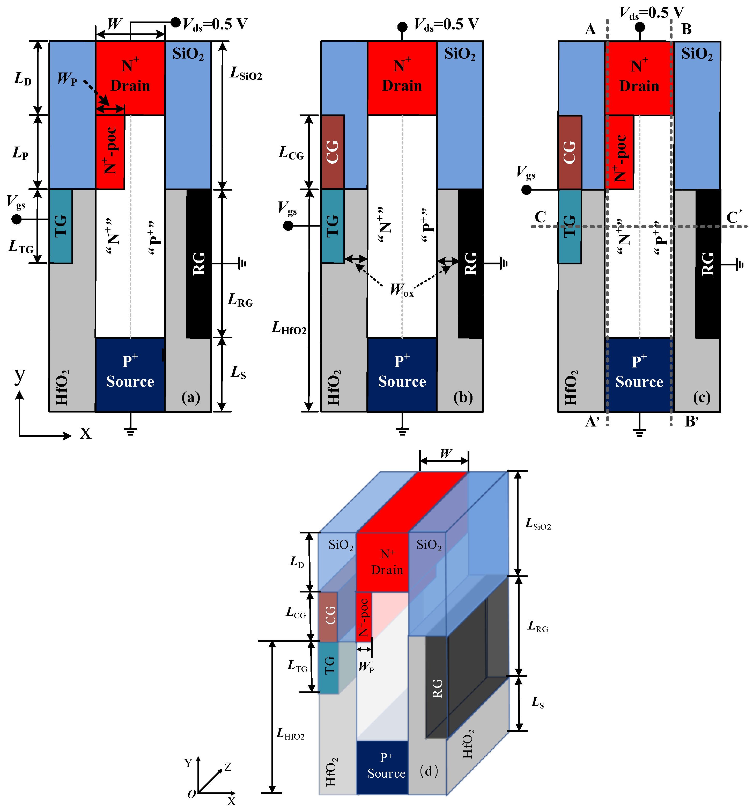
To better reveal the device mechanism of the proposed DGNP-EHBTFET, two other EHBTFETs are introduced in this paper: (1) an In0.53Ga0.47As EHBTFET with a dual-metal left-gate (DG-EHBTFET) and (2) an In0.53Ga0.47As EHBTFET with an N+-pocket (NP-EHBTFET). Cross-sectional views of these three vertical-structure EHBTFETs and a 3D schematic of DGNP-EHBTFET are shown in Figure 1, and the corresponding structural parameters are listed in Table 1.
For these three EHBTFETs, the structural parts are the same except for the left-gate and the channel region connected to the drain region. The left-gates of DG-EHBTFET and DGNP-EHBTFET are composed of a tunneling-gate (TG) and a control-gate (CG) tied directly, while that of NP-EHBTFET is only TG, and the N+-pocket connected with the drain region only exists in NP-EHBTFET and DGNP-EHBTFET. Based on the charge plasma concept [33,34], chromium with a work-function of 4.5 eV [35] is employed as TG to form an electron layer in the left-side channel near TG (i.e., the “N” region in Figure 1), and rhenium formed at a specified pressure and temperature (work-function = 5.5 eV) [36] can be picked as the grounded right-gate (RG) to create a hole layer in the right-side channel near RG (i.e., “P” region in Figure 1), so as to provide conditions for LT parallel to the gate electric field. To enhance electron tunneling and effectively suppress gate leakage and the ambipolar current, a HfO2/SiO2 heterogate dielectric is adopted in the proposed EHBTFET, which is widely used in TFETs [9,11,14]. Moreover, P-type doping with a concentration of 1 × 1019 cm−3 is carried out in the source region, while N-type doping with a concentration of 1 × 1019 cm−3 and 2 × 1019 cm−3 is performed in the drain region and the N+-pocket, respectively. Except for the source, the drain, and the N+-pocket regions, the other parts of the channel are intrinsic. In simulations, some key material parameters for In0.53Ga0.47As—the band gap, heavy-hole effective mass, light-hole effective mass, and electron effective mass—are 0.751 eV, 0.457 m0, 0.052 m0, and 0.042 m0, respectively [30,37].
The Silvaco Atlas 2D numerical simulation platform is used for all device simulations. To more accurately model the tunneling process, the non-local band-to-band (BTBT) tunneling model is adopted, which considers the spatial variation in the energy bands. The Lombardi mobility model with a remote coulomb scattering term is employed to account for the mobility degradation that occurs inside the inversion layers. Considering that the introduction of the HfO2 dielectric will generate a large number of traps at the HfO2/InGaAs interface, we adopt the trap-assisted tunneling model in simulations, and a single donor trap level is assumed near the valence band with an interface trap density of 1 × 1013 cm−2 eV−1. The limitation of this approach is that it cannot reflect the effect of the midlevel position of traps, which may over- or under-estimate SS and IOFF. In light of the quantum confinement effect in a thin channel layer, we adopt the density gradient model. Additionally, the Shockley–Read–Hall and Auger recombination models, drift-diffusion current transport model, bandgap-narrowing models, Fermi–Dirac carrier statistics, and Schenk oxide-tunneling model are included in the simulations. For these three EHBTFETs, corresponding physical quantities used for revealing some physical mechanisms can be extracted along cutlines A–A’, B–B’, and C–C’ (see dotted lines in Figure 1c), respectively. During data processing, IOFF and ION are extracted from the transfer characteristic curves in the OFF-state (Vgs = 0 V and Vds = 0.5 V) and ON-state (Vgs = 1 V and Vds = 0.5 V), respectively.
The proposed DGNP-EHBTFET can be manufactured by state-of-the-art process technology. A brief process flow for obtaining DGNP-EHBTFET is as follows. In stage (1), the In0.53Ga0.47As epitaxial layer is grown vertically on InP substrate using the molecular-beam epitaxy technique. P+-source, N+-pocket, and N+-drain are formed via ion implantation. Then, the epitaxial layer is etched using reactive ion etching or inductively coupled plasma etching in stage (2). To obtain the required N+-pocket and channel width, the key process focuses on the accurate design of the mask pattern. In stage (3), HfO2 can be deposited using the atomic layer deposition technique, followed by the etching of dielectrics and metal electrode deposition in stage (4). Finally, SiO2 deposition is carried out in stage (5). Moreover, to reduce the interface trap in real operation, good quality of the HfO2/InGaAs interface should be possessed, which can be realized through adoption of the Al2O3/HfO2 stack and the assurance of a good manufacturing process [38,39].
3. Results and Discussion
3.1. Operating Mechanism of Three EHBTFETs
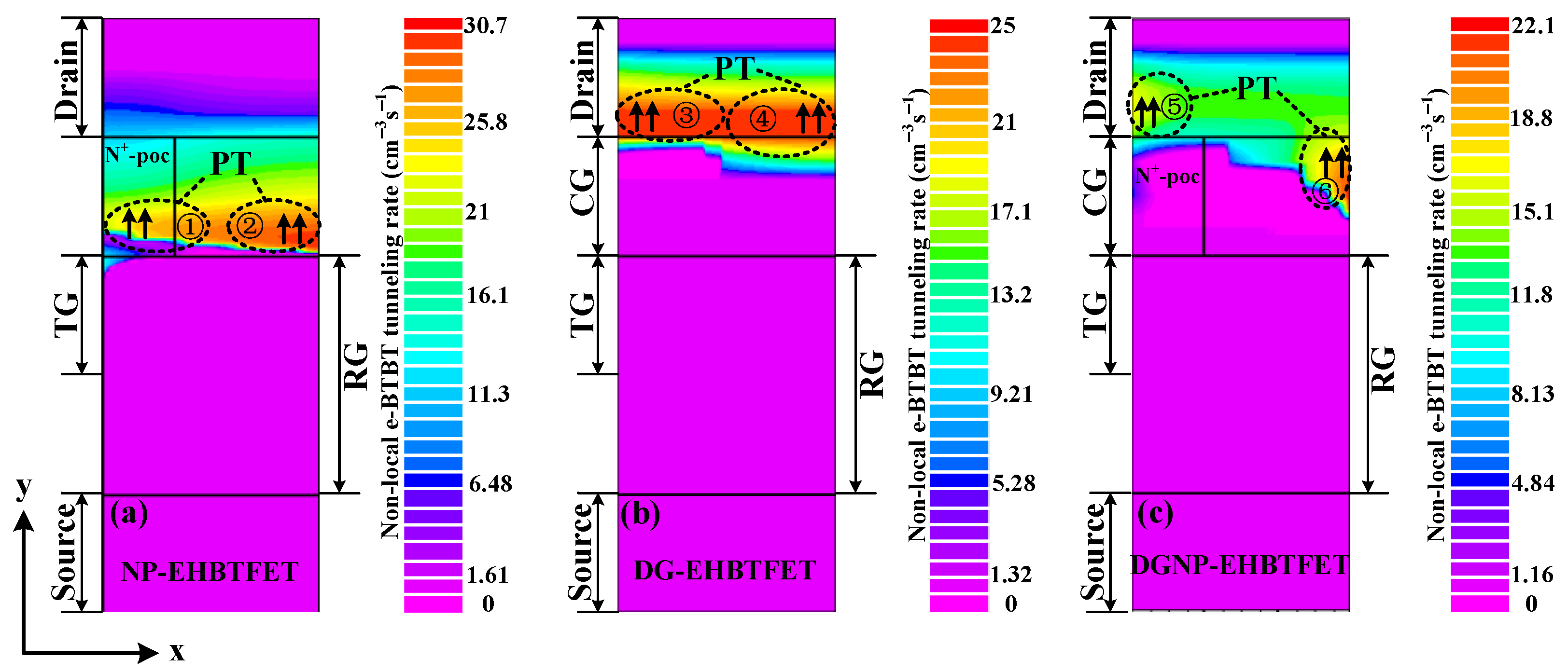
The operating mechanisms of NP-EHBTFET, DG-EHBTFET, and DGNP-EHBTFET can be interpreted using the non-local e-BTBT tunneling rate. For a clear explanation, we simulate the non-local e-BTBT tunneling rates for these three EHBTFETs from the perspective of vertical tunneling and lateral tunneling, respectively, with the results are shown in Figure 2 and Figure 3. Figure 2 shows the vertical non-local e-BTBT tunneling rate in the OFF-state. It is observed that vertical tunneling (see black arrows) appears above the gate overlap region between TG and RG for NP-EHBTFET (see black dotted circles ➀ and ➁). It is because of the existence of N+-pocket that the energy band of this region bends downward, so as to provide conditions for vertical tunneling. As shown in Figure 2b, the CG in DG-EHBTFET can induce holes in its right-side region, which forms a PN junction between this region and the drain region, and eventually results in vertical tunneling in black dotted circles ➂ and ➃. Figure 2c shows that the vertical tunneling of DGNP-EHBTFET mainly occurs in black dotted circles ➄ and ➅, and its non-local e-BTBT tunneling rate is lower than that of NP-EHBTFET and DG-EHBTFET. Thus, it can be seen that the simultaneous introduction of the CG and N+-pocket in DGNP-EHBTFET contributes to the suppression of vertical tunneling in the OFF-state. This is mainly due to their regulation of electron and hole concentrations in the gate underlap region near the drain. Since there is no lateral tunneling in these EHBTFETs in the OFF-state, it is concluded that vertical tunneling dominates in this state.
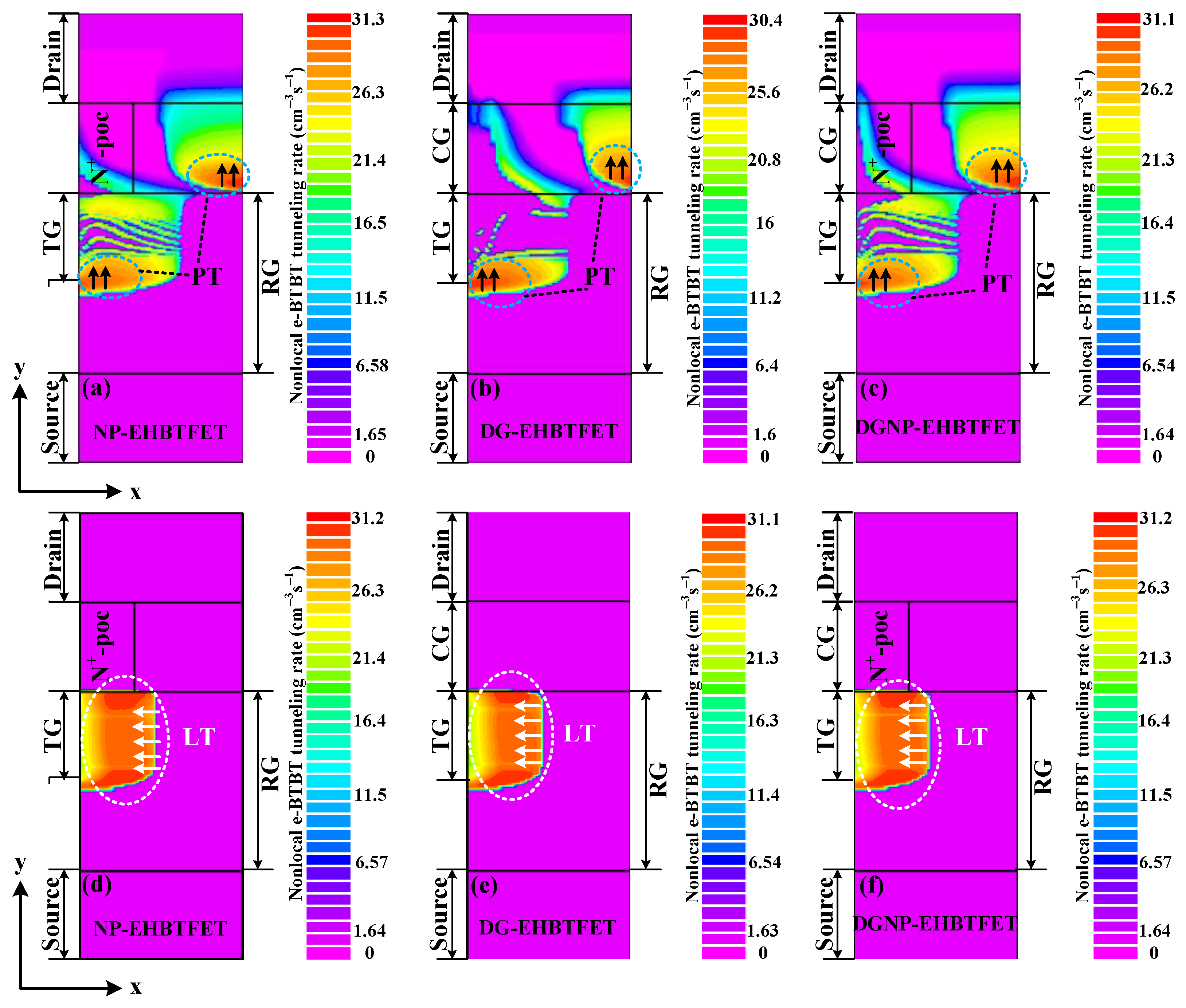
It is observed from Figure 3 that the distribution ranges of vertical tunneling for these three EHBTFETs (see green dotted circles in Figure 3a–c) are basically the same in the ON-state, which is due to the fact that Vgs applied to TG turns on electron tunneling in the left side of the source and the gate overlap region near RG. As shown in Figure 3d–f, since the TG and RG are the same for these three EHBTFETs, an identical electron–hole bilayer can be induced in the gate overlap region. In the ON-state, electrons tunnel from the valence band of the hole layer into the conduction band of the electron layer under the action of Vgs. Therefore, lateral tunneling (see white arrows in Figure 3d–f) also exists in these three EHBTFETs. Through comparison, we can see that the region available for vertical tunneling is only a few nanometers wide, so can be named PT, while that for lateral tunneling covers the entire gate overlap region (50 nm in length), so can be named LT. Combining the non-local e-BTBT tunneling rate of these two types of tunneling, it follows that LT dominates in the ON-state but PT does in the OFF-state.
3.2. Comparison of DC Performance among Three EHBTFETs
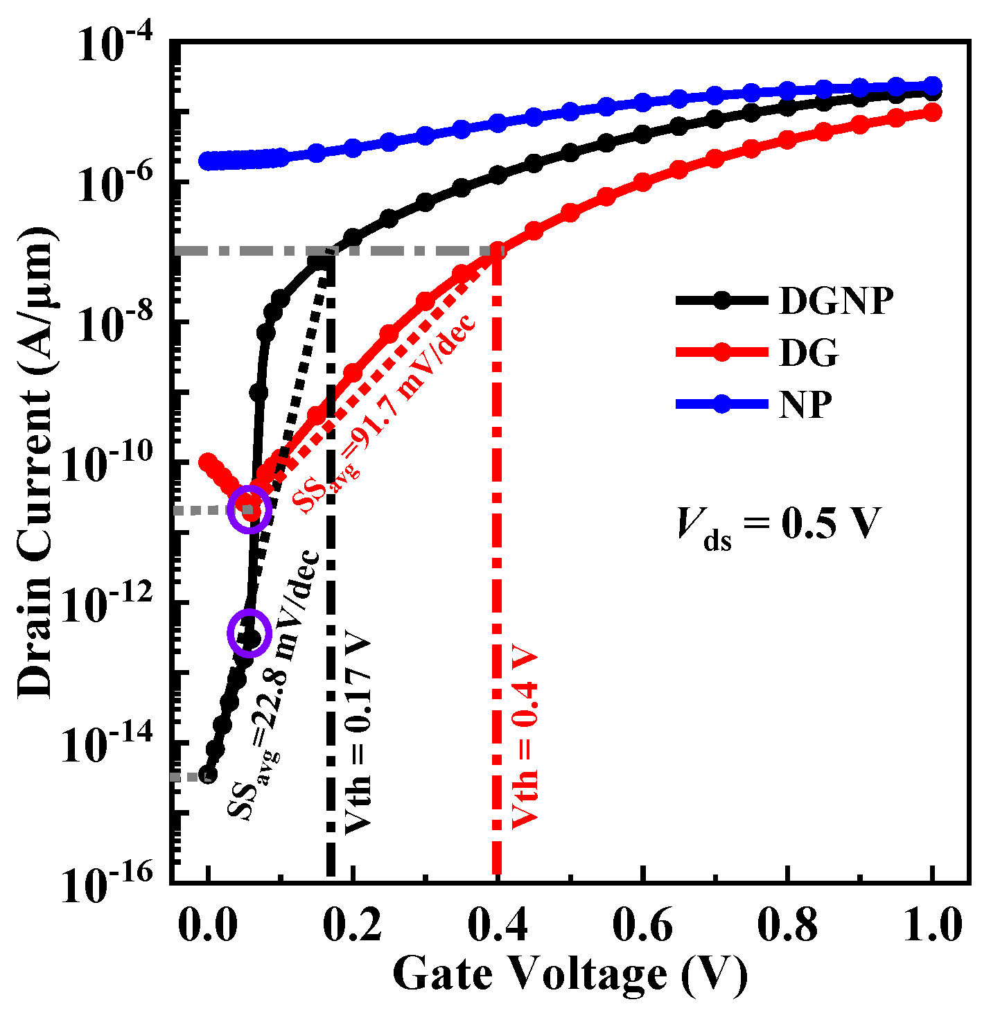
To compare DC performance, the transfer characteristics of DG-EHBTFET, NP-EHBTFET, and DGNP-EHBTFET are calculated and plotted in Figure 4. It is found from the figure that the IOFF of the proposed DGNP-EHBTFET is 3.54 × 10⁻¹⁵ A/μm, which is about four and nine orders of magnitude lower than that of DG-EHBTFET and NP-EHBTFET (9.9 × 10⁻¹¹ A/μm and 1.97 × 10⁻⁶ A/μm), respectively. The ION of DGNP-EHBTFET is close to 1.92 × 10⁻⁵ A/μm, almost the same magnitude as that of NP-EHBTFET but higher than that of DG-EHBTFET. Therefore, the maximum ION/IOFF can be obtained by DGNP-EHBTFET, and its value is 5.42 × 10⁹.
The tunneling current depends on the tunneling probability (Ptun), which can be expressed as Equation (1) [14]
where Δφ is the energy range used for carrier tunneling, E is the electric field, m* is the effective carrier mass, λ is the tunneling distance, Eg is the band gap, and εdie, εsem, tdie, and tsem are the permittivity and the thickness of the dielectric and the bulk material, respectively. Since Ptun is closely related to Δφ and E, we can interpret the difference between IOFF and ION for these three EHBTFETs based on them.
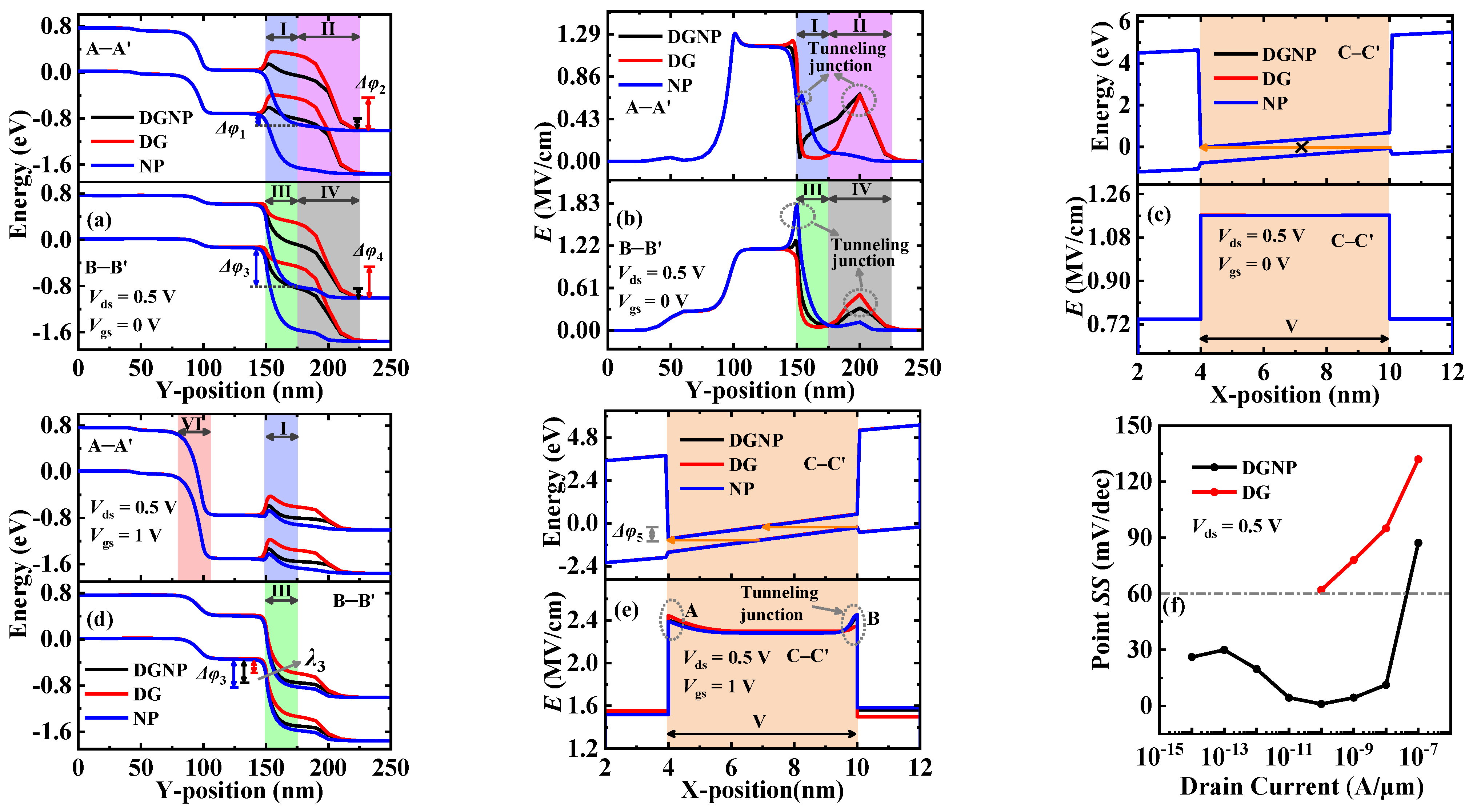
Figure 5 shows the energy band and the electric field profiles extracted along cutlines A–A’, B–B’, and C–C, respectively, in the OFF- and ON-states. To explain the physical mechanism more clearly, six regions (i.e., regions I to VI) are defined in the figures of this paper. This is because two kinds of tunneling mechanisms (PT and LT) exist in these three EHBTFETs, which occur in different regions based on different devices and states (see Figure 2 and Figure 3). As shown in Figure 5a, in the OFF-state, PT in NP-EHBTFET occurs in regions I and III, while that in DG- and DGNP-EHBTFETs occurs in regions II and IV. This is because the alignment of the conduction band and the valence band in these regions makes the energy range Δφ (named Δφ1 to Δφ6 in regions I to VI, respectively) that is available for carrier tunneling exist in regions I and III of NP-EHBTFET and regions II and IV of the other two EHBTFETs, respectively. Actually, the position of Δφ in DG-EHBTFET and DGNP-EHBTFET is different from that in NP-EHBTFET because the introduction of the control-gate CG lifts the energy band near it so as to shift the tunneling junction to the right. Moreover, for DGNP-EHBTFET, the simultaneous introduction of the CG and the N+-pocket can optimize its energy band profiles in four regions, which makes it have the narrowest Δφ. For further analysis, the electric field profiles in the OFF-state are calculated and plotted in Figure 5b. Since tunneling cannot occur in the regions without Δφ, we only compare E at the tunneling junctions of the four regions (see dotted circles in Figure 5b). It is observed that E at the tunneling junction of regions I and II is basically the same, but is very different in regions III and IV, so it can be inferred that the difference in Ptun mainly depends on E in regions III and IV. Obviously, DGNP-EHBTFET possesses the lowest E of the tunneling junction. The lower the E and the narrower the Δφ, the lower the Ptun of DGNP-EHBTFET that can be obtained, according to Equation (1). Furthermore, in the OFF-state, the energy band and the electric field profiles based on LT are also calculated, as shown in Figure 5c. It is found that the identical Es exist in the region V for these three EHBTFETs, which can be explained by Equation (2), expressed as
Since the gate overlap region for these three EHBTFETs has the same dielectric and bulk materials, the same tdie, tsem, εdie, εsem, and Eg are possessed in this region. Moreover, Figure 5c shows that there is no Δφ available for LT. According to Equation (2), the same E should exist in region V. Although there is E in region V, Δφ is absent; thus, no LT appears. It is thus clear that PT is dominant in the OFF-state, eventually resulting in DGNP-EHBTFET with the lowest IOFF.
To investigate ION, the energy band profiles in the ON-state are calculated and shown in Figure 5d. It is seen that PT occurs in regions III and VI simultaneously because the applied Vgs bends down the energy bands in both regions. Due to the existence of CG, the energy bands of DG-EHBTFET are lifted obviously in regions I and III. The elevated energy band in region I hinders the tunneling electrons drifting to the drain, while that in region III reduces Δφ3 and increases λ3 so as to directly weaken the carrier tunneling, both of which lead to a reduction in the ION of DG-EHBTFET. Since the introduction of the N+-pocket can lower the energy bands in regions I and III, a high ION can be maintained in DGNP-EHBTFET like in NP-EHBTFET. In the ON-state, the existence of Δφ (see Δφ5 in Figure 5e) enhances the E of LT, which is consistent with the result in Equation (2). However, unlike E in the OFF-state, E in regions A and B (see dotted circles in Figure 5e) in the ON-state further increases. This is because PT also affects the E of LT in the gate overlap region. It is observed from Figure 5d that the raised energy band in region I of DG-EHBTFET causes a large number of tunneling electrons from region VI to concentrate in the gate overlap region near TG, eventually resulting in the highest E in its region A. However, the existence of the N+-pocket bends the energy band downward in region III for NP-EHBTFET and DGNP-EHBTFET, which is more conducive to the accumulation of holes in the gate overlap region near RG, leading to a higher presence of E in region B (i.e., tunneling junction) of these two EHBTFETs. The higher the E, the higher the ION that can be obtained. Therefore, the ION of three EHBTFETs results in the aforementioned results.
The average subthreshold swing (SSavg) is obtained using Equation (3) [9,14]
where the subthreshold voltage (Vth) represents Vgs at which the drain current (Ids) equals 0.1 μA/μm (i.e., IVth), VOFF is Vgs at which Ids begins to increase with Vgs, and IVOFF is the corresponding Ids when Vgs = VOFF. It is found from Figure 4 that neither the Vth nor SSavg of NP-EHBTFET can be extracted because NP-EHBTFET has been turned on in the OFF-state. Thus, only the values of SSavg and Vth for DG-EHBTFET and DGNP-EHBTFET are compared here. The Vth and SSavg of DGNP-EHBTFET are 0.17 V and 22.8 mV/decade, respectively, which are reduced by 57.5% and 75.1%, respectively, compared with DG-EHBTFET. Moreover, DGNP-EHBTFET exhibits VOFF and IVOFF values approaching 0 V and 3.54 × 10⁻¹⁵ A/μm, respectively, lower than those of DG-EHBTFET. In particular, its IVOFF is four orders of magnitude lower than that of DG-EHBTFET, which is because PT, known from the previous analysis, is dominant in the OFF-state. For these two EHBTFETs, LT begins to operate when Vgs is applied to the left-gate, and its influence on Ids starts to exceed PT when Vgs > 0.06 V (see Ids distortion in the purple circles in Figure 4). Since the introduction of the N+-pocket can enhance the built-in electric field in the electron–hole bilayer so as to boost the Ptun of LT, IVth can be achieved under lower Vth for DGNP-EHBTFET, which is consistent with the results in Figure 4. As a result, a smaller difference between Vth and VOFF and a greater one between IVth and IVOFF exists in DGNP-EHBTFET, leading to a lower SSavg in it. Point SS at each Ids is expressed as dVgs/d(logIds). To clearly exhibit the change in SS, point SS values are extracted from the transfer characteristic curves and plotted in Figure 5f. Note that the point SS values of NP-EHBTFET cannot be extracted, and the reason is the same as for SSavg extraction. It is observed from the figure that the proposed DGNP-EHBTFET has steeper point SS when Vgs < Vth, and its minimum point SS is as low as 1.1 mV/decade. Based on above analyses, DGNP-EHBTFET possesses better DC performance.
SSavg = (Vth − VOFF)/(log IVth − log IVOFF),
3.3. Effect of N+-Pocket on DGNP-EHBTFET
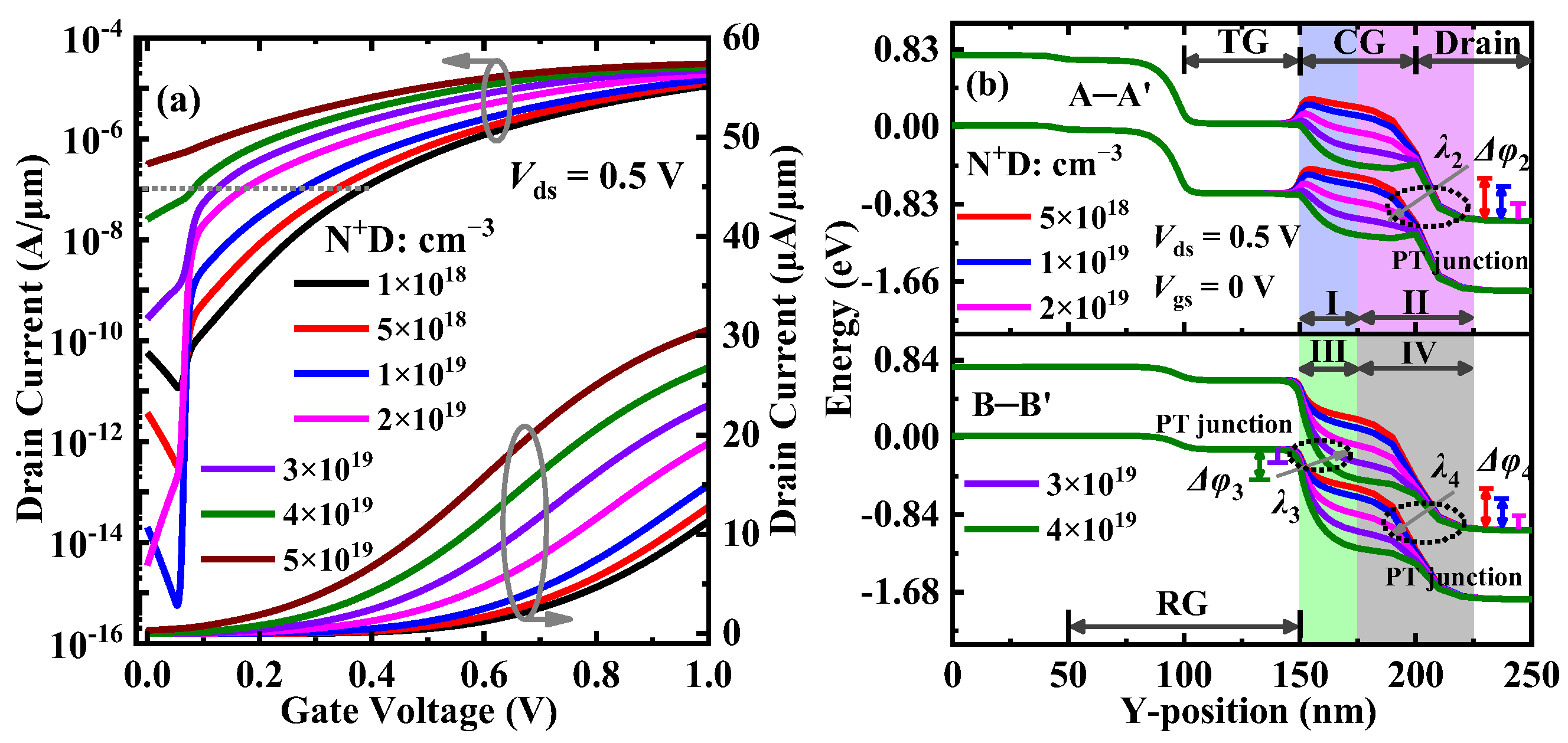
Figure 6a shows the transfer characteristics of DGNP-EHBTFET with the N+-pocket having a different N-type doping concentration (N+D). It is found from the figure that IOFF decreases first, and then, increases with the increase in N+D, and achieves the minimum value at N+D = 2 × 1019 cm−3. To interpret the variation in IOFF, the energy band profiles in the OFF-state are calculated and shown in Figure 6b. It is observed from Δφ that PT appears in regions II and IV when N+D ≤ 2 × 1019 cm−3 while the same occurs in region III when N+D > 2 × 1019 cm−3. With the increase in N+D, both Δφ2 and Δφ4 decrease but Δφ3 increases. Though Ptun can be reduced by narrowing Δφ to obtain a lower IOFF, λ (named λ1 to λ6 in regions I to VI, respectively) should also be taken into account according to Equation (1). Unlike λ in region III, those in regions II and IV increase with N+D, and their lengths are greater. Hence, one can see that the maximum λ and the minimum Δφ simultaneously exist when N+D = 2 × 1019 cm−3, thereby resulting in the minimum Ptun based on Equation (1), eventually obtaining the minimum IOFF. In fact, the change in the trend of IOFF is dependent on the position of the PT junction (see black dotted circles in Figure 6b). Since CG can induce holes in the top gate underlap region, PN junctions available for tunneling (i.e., the PT junction in regions II and IV) can be created between this region and the drain region. With there is an increase in N+D, the increasing electrons in the top gate underlap region bend the energy band downward so as to reduce the aligned energy range for tunneling, eventually degrading IOFF. When N+D > 2 × 1019 cm−3, the PT junction shifts to region III because a new PN junction is formed by electron accumulation in the top gate underlap region and hole accumulation in the gate overlap region near RG. With the further increase in N+D, more electrons gather in the top gate underlap region, which enlarges Δφ so as to promote the electron tunneling. Therefore, IOFF exhibits an increasing trend. Moreover, further investigation reveals that there is basically no impact of the variation in N+D on LT in the OFF-state. With the increase in N+D, ION values exhibit a similar trend of linear increase and are in the same order of magnitude, which is because the electric field at the LT junction is slightly adjusted with the change in N+D on the basis of the same electron–hole bilayer. It can also be found from Figure 6a that the lower the Vgs, the greater the influence of N+D on Ids. This is because at low Vgs, LT mainly depends on the built-in electric field in the electron–hole bilayer, which can be enhanced with an increase in N+D. A stronger built-in electric field will cause a higher Ptun of LT so as to turn on DGNP-EHBTFET more easily. Therefore, with the increase in N+D, Vth takes on a linear decreasing trend, except that it cannot be extracted when N+D = 5 × 1019 cm−3. ION/IOFF exhibits the opposite trend to IOFF, and approaches the maximum value of 5.42 × 10⁹ at N+D = 2 × 1019 cm−3. Benefiting from the minimum IVOFF and the low Vth, the minimum SSavg is reached when N+D = 2 × 1019 cm−3. As a result, the optimal device performance can be obtained at N+D = 2 × 1019 cm−3.
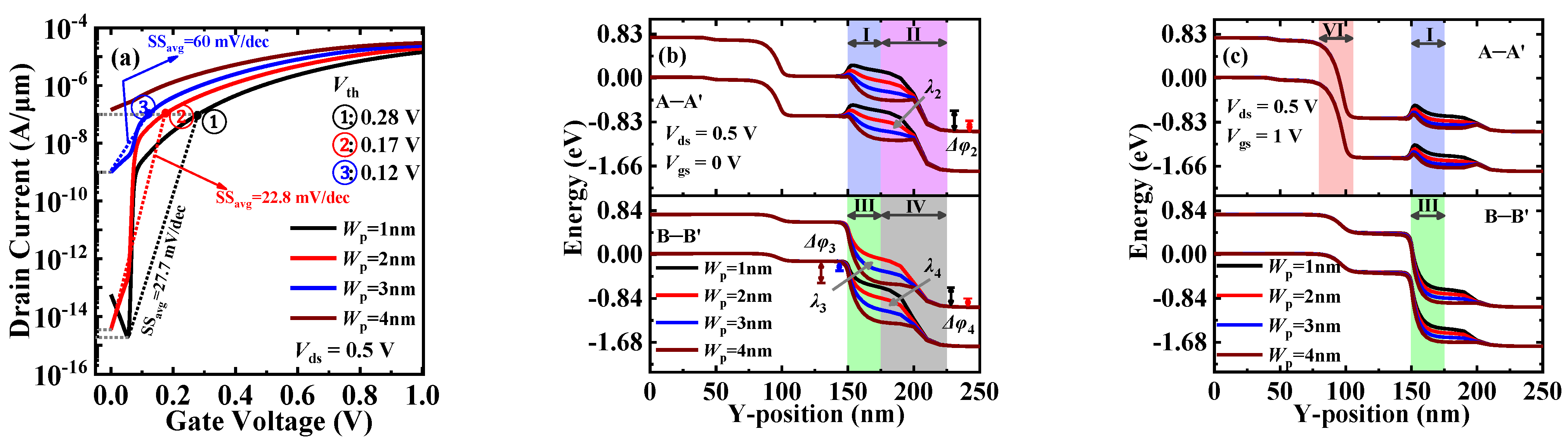
Next, the influence of the width of the N+-pocket (Wp) on the DC performance is studied. Figure 7a shows the transfer characteristic curves of DGNP-EHBTFET at Wp = 1~4 nm, from which various DC parameters such as IOFF, Vth, SSavg, etc., can be extracted. By compromising these extracted parameters, it follows that DGNP-EHBTFET possesses the optimal DC performance at Wp = 2 nm. Meanwhile, it is found that Figure 7a and Figure 6a have the same change trend in different cases, which is because Wp and N+D have identical mechanisms of influence on DGNP-EHBTFET. For example, it is observed from Figure 7b that PT occurs in regions II and IV when Wp ≤ 2 nm, while it occurs in region III when Wp > 2 nm. Similarly, DGNP-EHBTFET is of the maximum λ and the minimum Δφ at Wp = 2 nm, which makes it have the minimum IOFF under this condition. As shown in Figure 7c, the energy bands in regions I and III gradually bend downward with the increase in Wp, which promotes the drift of tunneling electrons in region VI and the tunneling of electrons in region III, respectively. However, a slight influence of Wp on LT is dominant in the ON-state; thus, ION increases with Wp but has the same order of magnitude.
3.4. Effect of Gate Work-Function on DGNP-EHBTFET
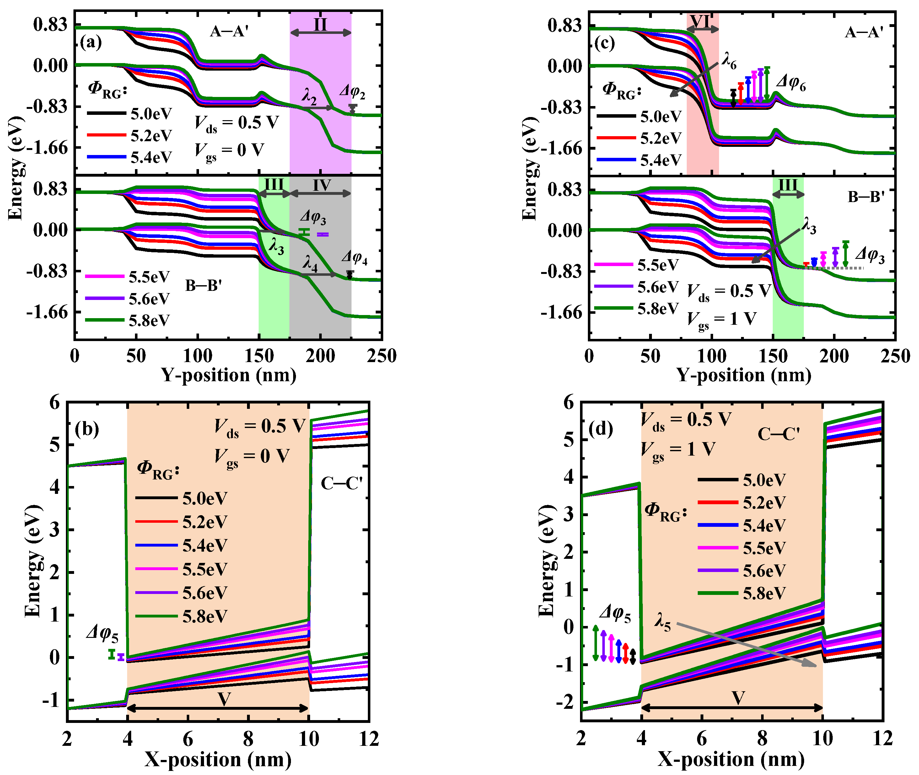
Here, we investigate the effect of the work-functions of the right-gate RG, the tunneling-gate TG, and the control-gate CG (i.e., ΦRG, ΦTG, and ΦCG, respectively) on DGNP-EHBTFET, respectively. Table 2 shows the extracted parameters at ΦRG = 5.0~5.8 eV. It is found that IOFF maintains a relatively low value at ΦRG ≤ 5.5 eV, but boosts sharply by six orders of magnitude with the further increase in ΦRG, which can be seen in the energy band profiles. As shown in Figure 8a, PT occurs in regions II and IV is exactly the same under different ΦRG levels. Moreover, because the hole concentration near RG increases with ΦRG so as to lift the energy bands in region III, PT can also take place in this region when ΦRG > 5.5 eV. Since narrow Δφ and wide λ exist in these tunneling regions, the effect of ΦRG on PT is insignificant in the OFF-state. Furthermore, it is observed from Figure 8b that LT is opened in region V when ΦRG > 5.5 eV. According to the changing trend of IOFF, it can be concluded that when ΦRG > 5.5 eV, the rapid increase in IOFF is mainly caused by LT. Figure 8c,d show the energy band profiles in the ON-state regarding PT and LT, respectively. It is seen that with the decrease in ΦRG, Δφ reduces but λ increases in regions III, V, and VI, particularly when ΦRG = 5.0 eV, and there is no tunneling in region III. Therefore, ION shows a monotonic decreasing trend with the reduction in ΦRG and achieves the minimum value at ΦRG = 5.0 eV. Both SSavg and Vth cannot be extracted at ΦRG = 5.0 eV as DGNP-EHBTFET is still turned off, even when Vgs = 1.0 V. Note that parameters that cannot be extracted in this paper are all represented by N/A. Moreover, with the increase in ΦRG, ION/IOFF represents a trend of increasing first, and then, decreasing, and Vth exhibits the opposite trend to ION. By comparing these parameters, we assume that DGNP-EHBTFET can maintain better device performance when ΦRG = 5.5 eV.
Table 3 lists the parameters extracted from the transfer characteristic curves at different ΦTG levels. It is found that with the increase in ΦTG, IOFF decreases first, and then, increases, and obtains the minimum value when ΦTG = 4.5 eV. To explain in detail, the energy band profiles of LT and PT are calculated. As shown in Figure 9a, when ΦTG < 4.5 eV, the accumulation of a large number of electrons near TG opens LT in the OFF-state; thus, the IOFF values are much higher than that in other cases. In addition, with the increase in ΦTG, Δφ5 decreases and λ5 increases, resulting in a gradual reduction in IOFF. When ΦTG ≥ 4.5 eV, IOFF is dependent on PT, which makes it have a substantial reduction. Since ΦTG just affects the carrier concentration of the gate overlap region (i.e., region V), only the energy bands in this region and the regions connected to it will be adjusted with the change in ΦTG. It is observed from Figure 9b that the energy bands in region III lift with the increase in ΦTG, and a new PT appears in this region when ΦTG > 4.6 eV; therefore, IOFF begins to increase obviously. It is found from Figure 9c that when ΦTG < 5.5 eV, LT is dominant in the ON-state, and ION shows a slowly decreasing trend with increasing ΦTG based on the variation in Δφ5 and λ5. It is worth noting that only PT exists when ΦTG = 5.5 eV, and it appears in regions I and III (not shown). As a result, the minimum ION is obtained at this ΦTG. Furthermore, the optimal values of ION/IOFF and SSavg can be obtained at ΦTG = 4.5 eV. Comprehensive analysis shows that ΦTG = 4.5 eV is the best choice for DGNP-EHBTFET.
Further, the influence of ΦCG on DGNP-EHBTFET is examined, and parameters related to DC performance are extracted and listed in Table 4. As shown in Figure 10a, since the variation in ΦCG can adjust the energy band profiles in regions I to IV, the region where PT appears varies with ΦCG. Because tunneling only exists in the regions with Δφ, we only compare E at the tunneling junction to explain the changing trend of IOFF. As shown in Figure 10b, when ΦCG < 4.5 eV, high E exists simultaneously at the tunneling junction of regions I and III, which results in a high IOFF and turns on DGNP-EHBTFET in the OFF-state. When ΦCG > 4.5 eV, E at the tunneling junction of regions II and IV increases with ΦCG, and there is also high E at the tunneling junction of region III at ΦCG = 4.9 eV. As a result, IOFF decreases first, and then, increases, and achieves the minimum IOFF at ΦCG = 5.0 eV. It is observed from Figure 10c that PT in region VI is insensitive to the change in ΦCG, but the energy band in region I elevates with the increase in ΦCG; especially when ΦCG > 4.5 eV it begins to hinder the drift of the tunneling electrons, eventually degrading device performance in the ON-state. Moreover, with the increase in ΦCG, E in the tunneling junction of region III gradually weakens, which reduces the Ptun of PT. As shown in Figure 10d, the varying trend of E at the LT junction of region V is the same as that in region III, thereby lowering the Ptun of LT with increasing ΦCG. Therefore, ION decreases with the increase in ΦCG, which is consistent with the results in Table 4. Furthermore, by comparison of the extracted parameters in Table 4, it follows that DGNP-EHBTFET can obtain optimal device performance only when ΦCG = 5.0 eV.
4. Conclusions
In conclusion, an In0.53Ga0.47As electron–hole bilayer TFET with a dual-metal left-gate and an N+-pocket is proposed and investigated in detail using the Silvaco Atlas 2D numerical simulation platform. The numerical simulations demonstrate that the simultaneous introduction of the control-gate and the N+-pocket for the proposed DGNP-EHBTFET can optimize the energy band profiles in the tunneling regions so as to substantially degrade the OFF-state current and maintain good ON-state performance. Further, the impact of the N+-pocket on DGNP-EHBTFET is investigated, and the results show that both N+D and Wp focus on the adjustment of the tunneling energy range and the tunneling distance of PT, thereby mainly affecting IOFF. By compromise of the extracted various parameters, the optimal DC performance can be obtained when N+D = 2 × 1019 cm−3 and Wp = 2 nm. Considering the change in ΦRG and ΦTG, it is observed that both can control LT and PT through the regulation of the carrier concentration in the overlap region, and comprehensive analysis illustrates that only when ΦRG = 5.5 eV and ΦTG = 4.5 eV can good device performance be maintained. Furthermore, the investigation shows that the variation in ΦCG can not only change the electric field of the tunneling junction, but it can also regulate and control the drift of tunneling electrons. The results show that ΦCG = 5.0 eV is the best choice for better DC performance. This paper focuses on revealing the OFF-state leakage suppression mechanism and optimizing the device parameters, without considering the static and dynamic behavior of the proposed DGNP-EHBTFET. In view of their importance, we will put emphasis on this aspect in our next work.
Author Contributions
Conceptualization, H.L., W.Z., Z.W., Y.L. and H.Z.; methodology, H.L. and W.Z.; software, H.L.; validation, Z.W. and H.L.; formal analysis, W.Z. and H.L.; investigation, Y.L. and H.L.; resources, H.Z. and H.L.; data curation, H.L.; writing—original draft preparation, H.L. and W.Z.; writing—review and editing, H.L. and Z.W.; visualization, H.L. and W.Z.; supervision, H.L.; project administration, H.L.; funding acquisition, H.L. and Y.L. All authors have read and agreed to the published version of the manuscript.
Funding
This research was funded by the National Natural Science Foundation of China (Grant No. 62264008), the Natural Science Foundation of Gansu Province (Grant No. 21JR7RA320), the Project of Construction of a strong Province with Intellectual Property Rights (Grant No. 20ZSCQ006), the Youth Program of the National Natural Science Foundation of China (Grant No. 61905102), and the Gansu Youth Science and Technology Fund Program (Grant No. 20JR5RA385).
Institutional Review Board Statement
Not applicable.
Informed Consent Statement
Not applicable.
Data Availability Statement
The data presented in this study are available on request from the corresponding author.
Conflicts of Interest
The authors declare no conflict of interest.
References
- Boucart, K.; Ionescu, A.M. Double-gate tunnel fet with high-κ gate dielectric. IEEE Trans. Electron. Devices 2007, 54, 1725–1733. [Google Scholar] [CrossRef]
- Ghosh, B.; Akram, M.W. Junctionless tunnel field effect transistor. IEEE Electron. Device Lett. 2013, 34, 584–586. [Google Scholar] [CrossRef]
- Kumar, M.J.; Janardhanan, S. Doping-less tunnel field effect transistor: Design and investigation. IEEE Trans. Electron. Devices 2013, 60, 3285–3290. [Google Scholar] [CrossRef] [Green Version]
- Kumar, N.; Raman, A. Performance Assessment of the Charge-Plasma-Based Cylindrical GAA Vertical Nanowire TFET with Impact of Interface Trap Charges. IEEE Trans. Electron. Devices 2019, 66, 4453–4460. [Google Scholar] [CrossRef]
- Gupta, A.K.; Raman, A.; Kumar, N. Design and Investigation of a Novel Charge Plasma-Based Core-Shell Ring-TFET: Analog and Linearity Analysis. IEEE Trans. Electron. Devices 2019, 66, 3506–3512. [Google Scholar] [CrossRef]
- Choi, Y.; Hong, Y.; Ko, E.; Shin, C. Optimization of double metal-gate InAs/Si heterojunction nanowire TFET. Semicond. Sci. Technol. 2020, 35, 075024. [Google Scholar] [CrossRef]
- Misra, R.; Singh, K.; Kumar, M.; Rastogi, R.; Kumar, A.; Dubey, S. An Ultra-Low-Power Black Phosphorus (B-Ph)/Si Heterojunction Dopingless-Tunnel FET (HD-TFET) with Enhanced Electrical Characteristics. Superlattices Microstruct. 2021, 149, 106752. [Google Scholar] [CrossRef]
- Tripathy, M.R.; Singh, A.K.; Samad, A.; Chander, S.; Baral, K.; Singh, P.K.; Jit, S. Device and Circuit-Level Assessment of GaSb/Si Heterojunction Vertical Tunnel-FET for Low-Power Applications. IEEE Trans. Electron. Devices 2020, 67, 1285–1292. [Google Scholar] [CrossRef]
- Liu, H.; Yang, L.A.; Jin, Z.; Hao, Y. An In0.53Ga0.47As/In0.52Al0.48As Heterojunction Dopingless Tunnel FET with a Heterogate Dielectric for High Performance. IEEE Trans. Electron. Devices 2019, 66, 3229–3235. [Google Scholar] [CrossRef]
- Pindoo, I.A.; Sinha, S.K.; Chander, S. Improvement of Electrical Characteristics of SiGe Source Based Tunnel FET Device. Silicon 2021, 13, 3209–3215. [Google Scholar] [CrossRef]
- Liu, H.; Yang, L.A.; Chen, Y.; Jin, Z.; Hao, Y. Performance enhancement of the dual-metal gate In0.53Ga0.47As dopingless TFET by using a platinum metal strip insertion. Jpn. J. Appl. Phys. 2019, 58, 104001. [Google Scholar] [CrossRef]
- Gedam, A.; Acharya, B.; Mishra, G.P. Junctionless Silicon Nanotube TFET for Improved DC and Radio Frequency Performance. Silicon 2021, 13, 167–178. [Google Scholar] [CrossRef]
- Raad, B.R.; Tirkey, S.; Sharma, D.; Kondekar, P. A new design approach of dopingless tunnel fet for enhancement of device characteristics. IEEE Trans. Electron. Devices 2017, 64, 1830–1836. [Google Scholar] [CrossRef]
- Liu, H.; Yang, L.A.; Zhang, H.W.; Zhang, B.T.; Zhang, W.T. An In0.53Ga0.47As/In0.52Al0.48As/In0.53Ga0.47As double hetero-junction junctionless TFET. Jpn. J. Appl. Phys. 2021, 60, 074001. [Google Scholar] [CrossRef]
- Xu, H.F.; Han, X.F.; Sun, W. Design and investigation of dopingless double-gate line tunneling transistor: Analog performance, linearity, and harmonic distortion analysis. Chin. Phys. B 2020, 29, 108502. [Google Scholar] [CrossRef]
- Ghosh, P.; Bhowmick, B. Investigation of Electrical Characteristics in a Ferroelectric L-Patterned Gate Dual Tunnel Diode TFET. IEEE Trans. Ultrason. Ferroelectr. Freq. Control 2020, 67, 2440–2444. [Google Scholar] [CrossRef]
- Xie, H.W.; Liu, H.X.; Han, T.; Li, W.; Chen, S.P.; Wang, S.L. TCAD Simulation of a Double L-shaped gate Tunnel Field Effect Transistor with covered source–channel. Micro Nano Lett. 2020, 15, 272–276. [Google Scholar] [CrossRef]
- Ahangari, Z. Performance investigation of steep-slope core–shell nanotube indium nitride electron–hole bilayer tunnel field effect transistor. Appl. Phys. A Mater. Sci. Process. 2019, 125, 405. [Google Scholar] [CrossRef]
- Kim, S.; Choi, W.Y.; Park, B.G. Vertical-Structured Electron-Hole Bilayer Tunnel Field-Effect Transistor for Extremely Low-Power Operation with High Scalability. IEEE Trans. Electron. Devices 2018, 65, 2010–2015. [Google Scholar] [CrossRef]
- Padilla, J.L.; Medina-Bailon, C.; Alper, C.; Gamiz, F.; Ionescu, A.M. Confinement-induced InAs/GaSb heterojunction electron–hole bilayer tunneling field-effect transistor. Appl. Phys. Lett. 2018, 112, 182101. [Google Scholar] [CrossRef]
- Masoudi, A.; Ahangari, Z.; Fathipour, M. Performance optimization of a nanoscale GaSb P-channel electron-hole bilayer tunnel field effect transistor using metal gate workfunction engineering. Mater. Res. Express 2019, 6, 096311. [Google Scholar] [CrossRef]
- Padilla, J.L.; Medina-Bailon, C.; Marquez, C.; Sampedro, C.; Donetti, L.; Gamiz, F.; Ionescu, A.M. Gate Leakage Tunneling Impact on the InAs/GaSb Heterojunction Electron-Hole Bilayer Tunneling Field-Effect Transistor. IEEE Trans. Electron. Devices 2018, 65, 4679–4686. [Google Scholar] [CrossRef]
- Ahangari, Z. Design and performance optimization of thin film tin monoxide (SnO)/silicon electron–hole bilayer tunnel field-effect transistor. J. Comput. Electron. 2020, 19, 1485–1493. [Google Scholar] [CrossRef]
- Shamloo, H.; Goharrizi, A.Y. Performance study of tunneling field effect transistors based on the graphene and phosphorene nanoribbons. Micro Nanostruct. 2022, 169, 207336. [Google Scholar] [CrossRef]
- Jiang, X.; Shi, X.; Zhang, M.; Wang, Y.; Zhang, D.W. A symmetric tunnel field-effect transistor based on mos2/black phosphorus/mos2 nanolayered heterostructures. ACS Appl. Nano Mater. 2019, 2, 5674–5680. [Google Scholar] [CrossRef]
- Jiao, X.; Jia, J.; Shen, L.; Ju, J.; Lee, S. Tunneling field effect transistor integrated with black phosphorus-mos2 junction and ion gel dielectric. Appl. Phys. Lett. 2017, 110, 033103. [Google Scholar]
- Iida, R.; Kim, S.H.; Yokoyama, M.; Taoka, N. Planar-type In0.53Ga0.47As channel band-to-band tunneling metal-oxide-semiconductor field-effect transistors. J. Appl. Phys. 2011, 110, 124505. [Google Scholar] [CrossRef]
- Ahn, D.H.; Yoon, S.H.; Takenaka, M.; Takagi, S. Effects of HfO2/Al2O3 gate stacks on electrical performance of planar InxGa1−xAs tunneling field-effect transistors. Appl. Phys. Express 2017, 10, 084201. [Google Scholar] [CrossRef]
- Seo, J.H.; Yoon, Y.J.; Cho, S.; Kang, I.M.; Lee, J.H. Design optimization and analysis of ingaas/inas/ingaas heterojunction-based electron hole bilayer tunneling fets. J. Nanosci. Nanotechnol. 2019, 19, 6070–6076. [Google Scholar] [CrossRef]
- Alper, C.; Palestri, P.; Padilla, J.L.; Ionescu, A.M. The Electron-Hole Bilayer TFET: Dimensionality Effects and Optimization. IEEE Trans. Electron. Devices 2016, 63, 2603–2609. [Google Scholar] [CrossRef] [Green Version]
- Alper, C.; Palestri, P.; Padilla, J.L.; Ionescu, A.M. Underlap counterdoping as an efficient means to suppress lateral leakage in the electron–hole bilayer tunnel FET. Semicond. Sci. Technol. 2016, 31, 045001. [Google Scholar] [CrossRef]
- Loan, S.A.; Alharbi, A.G.; Rafat, M. Ambipolar leakage suppression in electron–hole bilayer TFET: Investigation and analysis. J. Comput. Electron. 2018, 17, 977–985. [Google Scholar]
- Sahu, C.; Singh, J. Charge-Plasma Based Process Variation Immune Junctionless Transistor. IEEE Electron. Device Lett. 2014, 35, 411–413. [Google Scholar] [CrossRef]
- Hueting, R.J.E.; Rajasekharan, B.; Salm, C.; Schmitz, J. The Charge Plasma P-N Diode. IEEE Electron. Device Lett. 2008, 29, 1367–1369. [Google Scholar] [CrossRef] [Green Version]
- Lide, D.R. CRC Handbook of Chemistry and Physics, 89th ed.; Taylor and Francis: New York, NY, USA, 2008; p. 12. [Google Scholar]
- Kawano, H.; Takahashi, T.; Tagashira, Y.; Mine, H.; Moriyama, M. Work function of refractory metals and its dependence upon working conditions. Surf. Sci. 1999, 146, 105–108. [Google Scholar] [CrossRef]
- Vurgaftman, I.; Meyer, J.R.; Ram-Mohan, L.R. Band parameters for III–V compound semiconductors and their alloys. J. Appl. Phys. 2001, 89, 5815–5875. [Google Scholar] [CrossRef] [Green Version]
- Suzuki, R.; Taoka, N.; Yokoyama, M.; Lee, S.; Kim, S.H.; Hoshii, T.; Yasuda, T.; Jevasuwan, W.; Maeda, T.; Ichikawa, O.; et al. 1-nm-capacitance-equivalent-thickness HfO2/Al2O3/InGaAs metal-oxide-semiconductor structure with low interface trap density and low gate leakage current density. Appl. Phys. Lett. 2012, 100, 132906. [Google Scholar] [CrossRef]
- Zhao, H.; Chen, Y.; Wang, Y.; Zhou, F.; Xue, F.; Lee, J. InGaAs Tunneling Field-Effect-Transistors with Atomic-Layer-Deposited Gate Oxides. IEEE Trans. Electron. Devices 2011, 58, 2990–2995. [Google Scholar] [CrossRef]
Figure 1.
Cross sectional views of (a) NP-EHBTFET; (b) DG-EHBTFET; and (c) DGNP-EHBTFET. (d) A 3D schematic of DGNP-EHBTFET. Cutlines A–A’ and B–B’ are located at 0.5 nm on the right side of the left-gate dielectric and the left side of the right-gate dielectric, respectively, and cutline C–C’ is located in the middle of the tunneling-gate.

Figure 2.
Contour plots of the vertical non-local e-BTBT tunneling rate for (a) NP-EHBTFET; (b) DG-EHBTFET; and (c) DGNP-EHBTFET, in the OFF-state.
Figure 2.
Contour plots of the vertical non-local e-BTBT tunneling rate for (a) NP-EHBTFET; (b) DG-EHBTFET; and (c) DGNP-EHBTFET, in the OFF-state.

Figure 3.
Contour plots of the vertical non-local e-BTBT tunneling rate for (a) NP-EHBTFET; (b) DG-EHBTFET; and (c) DGNP-EHBTFET, in the ON-state. Contour plots of the lateral non-local e-BTBT tunneling rate for (d) NP-EHBTFET; (e) DG-EHBTFET; and (f) DGNP-EHBTFET, in the ON-state.
Figure 3.
Contour plots of the vertical non-local e-BTBT tunneling rate for (a) NP-EHBTFET; (b) DG-EHBTFET; and (c) DGNP-EHBTFET, in the ON-state. Contour plots of the lateral non-local e-BTBT tunneling rate for (d) NP-EHBTFET; (e) DG-EHBTFET; and (f) DGNP-EHBTFET, in the ON-state.

Figure 4.
Transfer characteristics of DG-EHBTFET, NP-EHBTFET, and DGNP-EHBTFET.

Figure 5.
(a) Energy band profiles along A–A’ and B–B’ in the OFF-state; (b) electric field profiles along A–A’ and B–B’ in the OFF-state; (c) energy band and electric field profiles along C–C’ in the OFF-state; (d) energy band profiles along A–A’ and B–B’ in the ON-state; (e) energy band and electric field profiles along C–C’ in the ON-state; and (f) point SS versus drain current for EHBTFETs.

Figure 6.
(a) Transfer characteristics and (b) energy band profiles along A–A’ and B–B’ in the OFF-state, for DGNP-EHBTFET with N+D = 5 × 10¹⁸~4 × 1019 cm−3.
Figure 6.
(a) Transfer characteristics and (b) energy band profiles along A–A’ and B–B’ in the OFF-state, for DGNP-EHBTFET with N+D = 5 × 10¹⁸~4 × 1019 cm−3.

Figure 7.
(a) Transfer characteristics; (b) energy band profiles along A–A’ and B–B’ in the OFF-state; and (c) energy band profiles along A–A’ and B–B’ in the ON-state, for DGNP-EHBTFET with Wp = 1~4 nm.
Figure 7.
(a) Transfer characteristics; (b) energy band profiles along A–A’ and B–B’ in the OFF-state; and (c) energy band profiles along A–A’ and B–B’ in the ON-state, for DGNP-EHBTFET with Wp = 1~4 nm.

Figure 8.
(a) Energy band profiles along A–A’ and B–B’ in the OFF-state; (b) energy band profiles along C–C’ in the OFF-state; (c) energy band profiles along A–A’ and B–B’ in the ON-state; and (d) energy band profiles along C–C’ in the ON-state, for DGNP-EHBTFET with ΦRG = 5.0~5.8 eV.
Figure 8.
(a) Energy band profiles along A–A’ and B–B’ in the OFF-state; (b) energy band profiles along C–C’ in the OFF-state; (c) energy band profiles along A–A’ and B–B’ in the ON-state; and (d) energy band profiles along C–C’ in the ON-state, for DGNP-EHBTFET with ΦRG = 5.0~5.8 eV.

Figure 9.
(a) Energy band profiles along C–C’ in the OFF-state; (b) energy band profiles along A–A’ and B–B’ in the OFF-state; and (c) energy band profiles along C–C’ in the ON-state, for DGNP-EHBTFET with ΦTG = 3.5~5.5 eV.
Figure 9.
(a) Energy band profiles along C–C’ in the OFF-state; (b) energy band profiles along A–A’ and B–B’ in the OFF-state; and (c) energy band profiles along C–C’ in the ON-state, for DGNP-EHBTFET with ΦTG = 3.5~5.5 eV.

Figure 10.
(a) Energy band profiles along A–A’ and B–B’ in the OFF-state; (b) electric field profiles along A–A’ and B–B’ in the OFF-state; (c) energy band profiles along A–A’ and electric field profiles along B–B’, in the ON-state; and (d) electric field profiles along C–C’ in the ON-state, for DGNP-EHBTFET with ΦCG = 3.5~5.5 eV.


Table 1.
Device structure parameters used in simulations.
| Parameters | Value |
|---|---|
| Bulk material width (W) | 6 nm |
| N+-pocket width (Wp) | 2 nm |
| N+-pocket length (Lp) | 50 nm |
| Drain length (LD) | 50 nm |
| Source length (LS) | 50 nm |
| Tunneling-gate length (LTG) | 50 nm |
| Control-gate length (LCG) | 50 nm |
| Right-gate length (LRG) | 100 nm |
| HfO2 length (LHfO2) | 150 nm |
| SiO2 length (LSiO2) | 100 nm |
| Dielectric width near gate (Wox) | 2 nm |
| Tunneling-gate work-function (ΦTG) | 4.5 eV |
| Control-gate work-function (ΦCG) | 5.0 eV |
| Right-gate work-function (ΦRG) | 5.5 eV |
Table 2.
Extracted parameters from transfer characteristic curves at ΦRG = 5.0~5.8 eV.
| ΦRG (eV) | IOFF (A/μm) | ION (A/μm) | ION/IOFF | Vth (V) | SSavg (mV/dec) |
|---|---|---|---|---|---|
| 5.0 | 1.50 × 10⁻¹⁹ | 1.87 × 10⁻⁸ | 1.25 × 10¹¹ | N/A | N/A |
| 5.2 | 1.15 × 10⁻¹⁸ | 1.20 × 10⁻⁶ | 1.04 × 10¹² | 0.52 | 30.7 |
| 5.4 | 2.59 × 10⁻¹⁷ | 5.79 × 10⁻⁶ | 2.24 × 10¹¹ | 0.32 | 33.4 |
| 5.5 | 3.54 × 10⁻¹⁵ | 1.92 × 10⁻⁵ | 5.42 × 10⁹ | 0.17 | 22.8 |
| 5.6 | 2.58 × 10⁻⁹ | 2.87 × 10⁻⁵ | 1.11 × 10⁴ | 0.14 | 88.1 |
| 5.8 | 5.16 × 10⁻⁹ | 4.30 × 10⁻⁵ | 8.33 × 10³ | 0.11 | 85.4 |
Table 3.
Extracted parameters from transfer characteristic curves at ΦTG = 3.5~5.5 eV.
| ΦTG (eV) | IOFF (A/μm) | ION (A/μm) | ION/IOFF | Vth (V) | SSavg (mV/dec) |
|---|---|---|---|---|---|
| 3.5 | 1.64 × 10⁻⁷ | 2.19 × 10⁻⁵ | 1.34 × 10² | N/A | N/A |
| 4.0 | 7.87 × 10⁻⁸ | 2.11 × 10⁻⁵ | 2.68 × 10² | 0.02 | 192.3 |
| 4.4 | 7.90 × 10⁻⁹ | 1.99 × 10⁻⁵ | 2.52 × 10³ | 0.12 | 108.9 |
| 4.5 | 3.54 × 10⁻¹⁵ | 1.92 × 10⁻⁵ | 5.42 × 10⁹ | 0.17 | 22.8 |
| 4.6 | 8.51 × 10⁻¹⁵ | 1.81 × 10⁻⁵ | 2.13 × 10⁹ | 0.24 | 33.9 |
| 5.0 | 1.03 × 10⁻¹³ | 9.93 × 10⁻⁶ | 9.64 × 10⁷ | 0.48 | 80.2 |
| 5.5 | 6.86 × 10⁻¹³ | 3.43 × 10⁻⁶ | 5.00 × 10⁶ | 0.51 | 98.8 |
Table 4.
Extracted parameters from transfer characteristic curves at ΦCG = 3.5~5.5 eV.
| ΦCG (eV) | IOFF (A/μm) | ION (A/μm) | ION/IOFF | Vth (V) | SSavg (mV/dec) |
|---|---|---|---|---|---|
| 3.5 | 1.47 × 10⁻⁵ | 4.57 × 10⁻⁵ | 3.11 × 100 | N/A | N/A |
| 4.0 | 3.43 × 10⁻⁶ | 3.79 × 10⁻⁵ | 1.10 × 101 | N/A | N/A |
| 4.5 | 9.13 × 10⁻⁸ | 2.90 × 10⁻⁵ | 3.18 × 10² | 0.02 | 506 |
| 4.9 | 4.39 × 10⁻¹² | 2.13 × 10⁻⁵ | 4.85 × 10⁶ | 0.14 | 32.1 |
| 5.0 | 3.54 × 10⁻¹⁵ | 1.92 × 10⁻⁵ | 5.42 × 10⁹ | 0.17 | 22.8 |
| 5.1 | 4.96 × 10⁻¹⁵ | 1.68 × 10⁻⁵ | 3.39 × 10⁹ | 0.23 | 31.5 |
| 5.5 | 7.04 × 10⁻¹⁰ | 6.37 × 10⁻⁶ | 9.05 × 10³ | 0.52 | 105 |
Publisher’s Note: MDPI stays neutral with regard to jurisdictional claims in published maps and institutional affiliations. |
© 2022 by the authors. Licensee MDPI, Basel, Switzerland. This article is an open access article distributed under the terms and conditions of the Creative Commons Attribution (CC BY) license (https://creativecommons.org/licenses/by/4.0/).
Share and Cite
MDPI and ACS Style
Liu, H.; Zhang, W.; Wang, Z.; Li, Y.; Zhang, H. OFF-State Leakage Suppression in Vertical Electron–Hole Bilayer TFET Using Dual-Metal Left-Gate and N+-Pocket. Materials 2022, 15, 6924. https://doi.org/10.3390/ma15196924
AMA Style
Liu H, Zhang W, Wang Z, Li Y, Zhang H. OFF-State Leakage Suppression in Vertical Electron–Hole Bilayer TFET Using Dual-Metal Left-Gate and N+-Pocket. Materials. 2022; 15(19):6924. https://doi.org/10.3390/ma15196924
Chicago/Turabian StyleLiu, Hu, Wenting Zhang, Zaixing Wang, Yao Li, and Huawei Zhang. 2022. "OFF-State Leakage Suppression in Vertical Electron–Hole Bilayer TFET Using Dual-Metal Left-Gate and N+-Pocket" Materials 15, no. 19: 6924. https://doi.org/10.3390/ma15196924
Note that from the first issue of 2016, this journal uses article numbers instead of page numbers. See further details here.