
Mode I Fatigue and Fracture Assessment of Polyimide–Epoxy and Silicon–Epoxy Interfaces in Chip-Package Components

 , ,
, , 
Abstract
:1. Introduction
2. Experimental Section
2.1. Materials
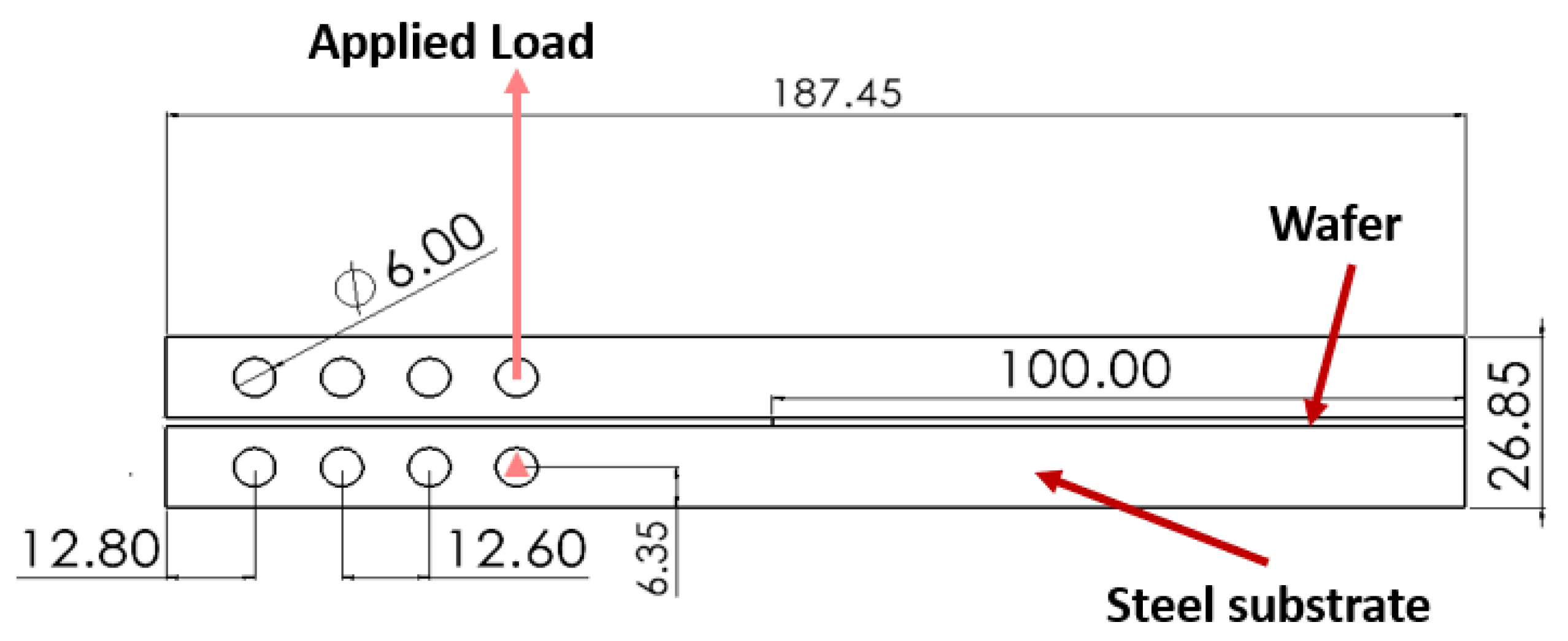
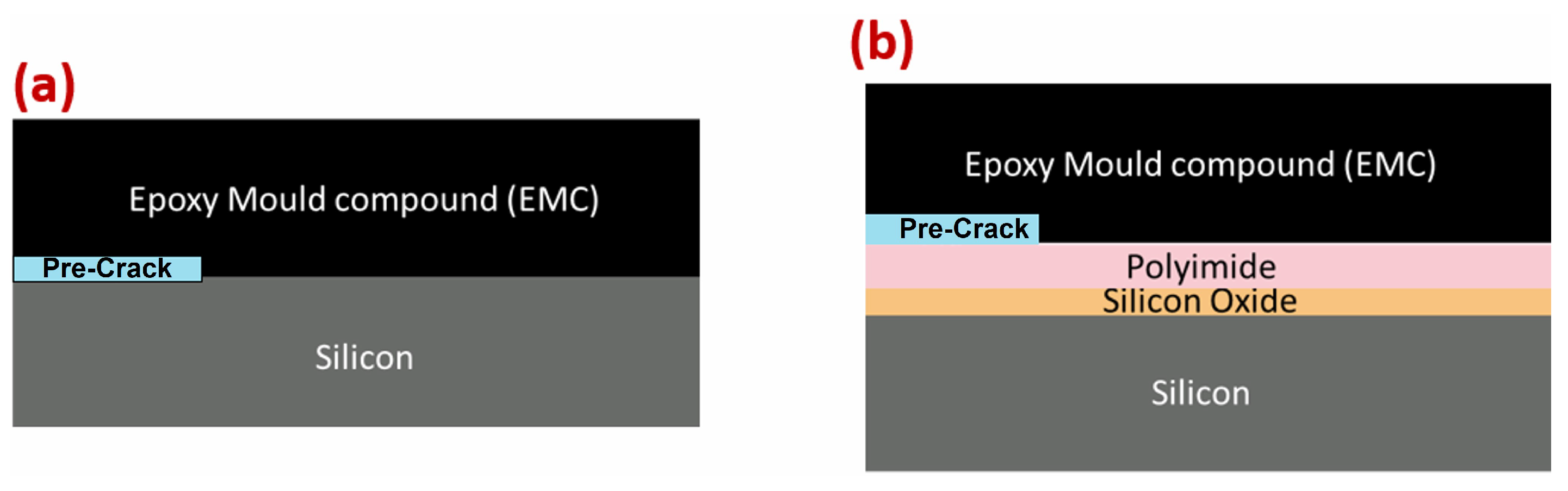
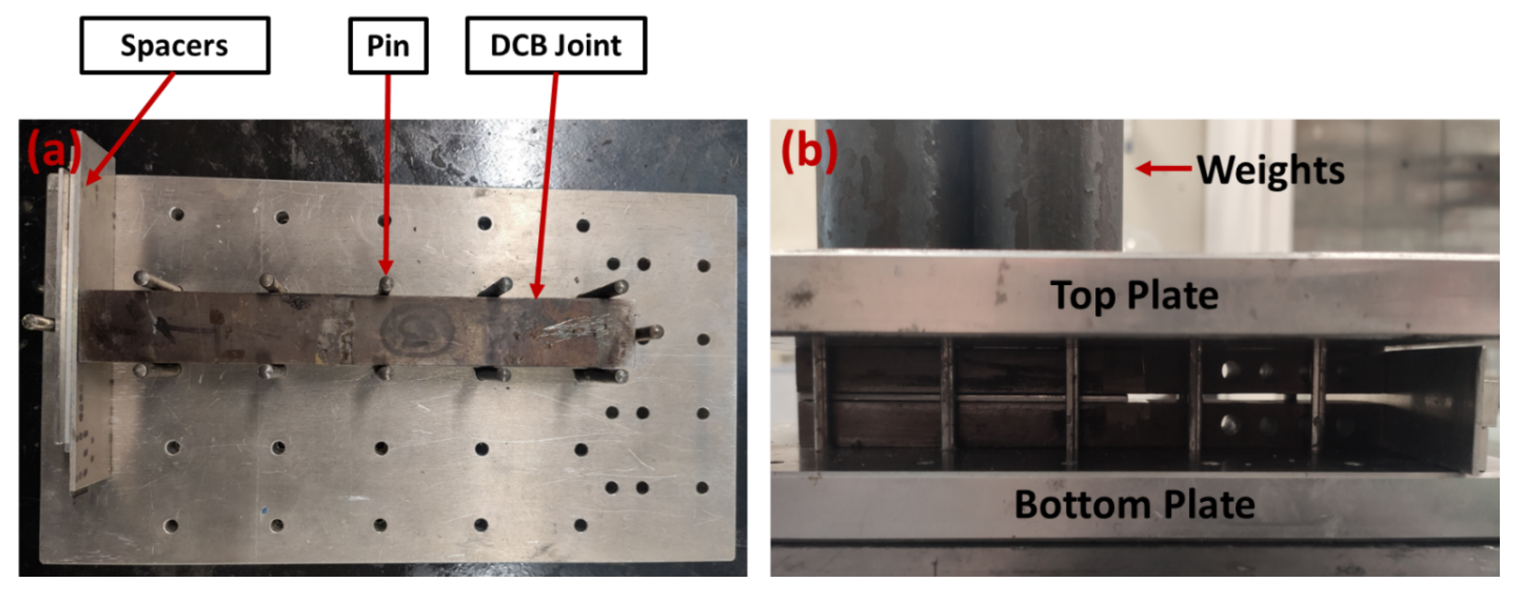
Specimen Manufacture and Geometry
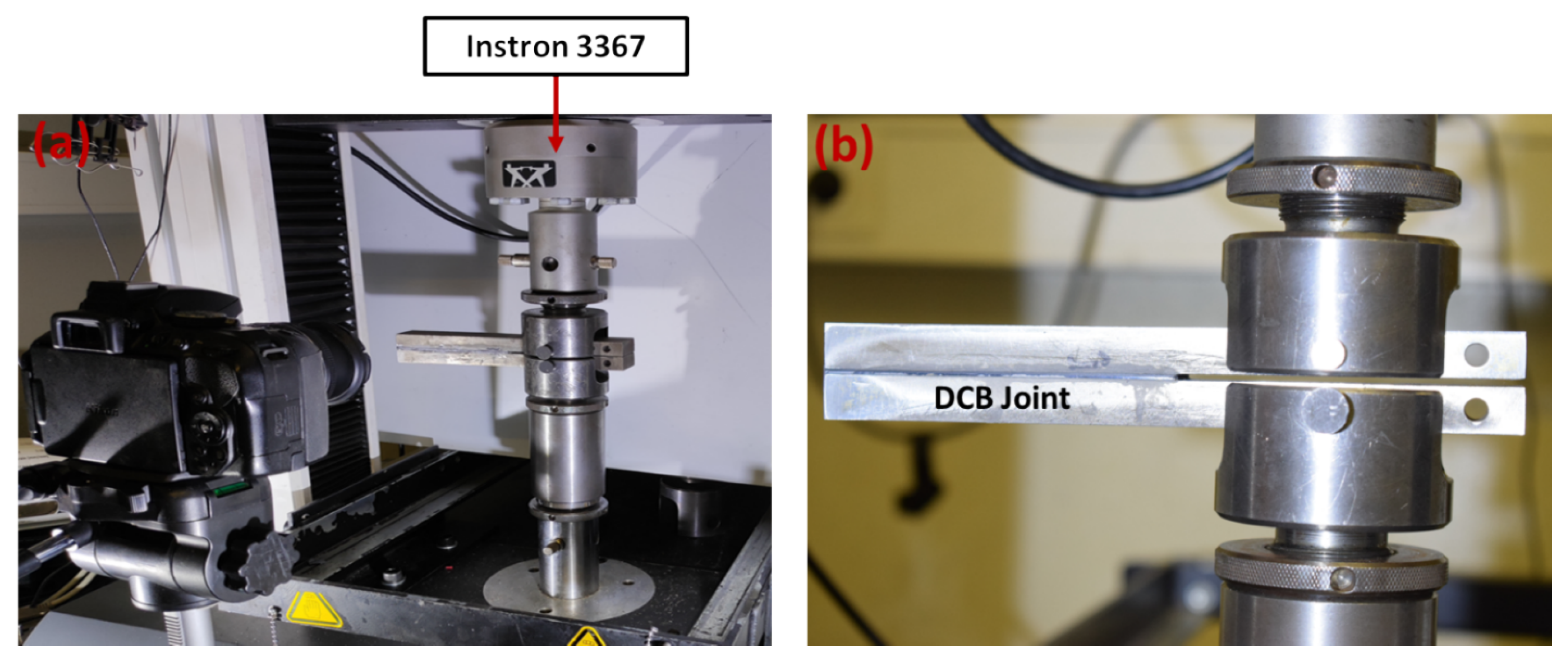
2.2. Test Procedure
2.3. Data Reduction Approach
2.4. Results and Discussion
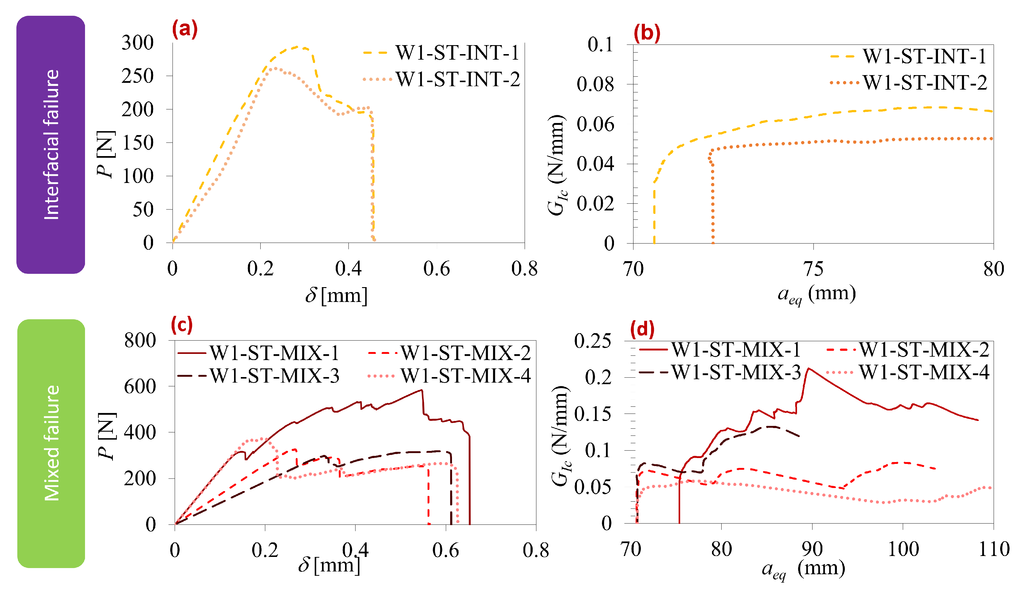
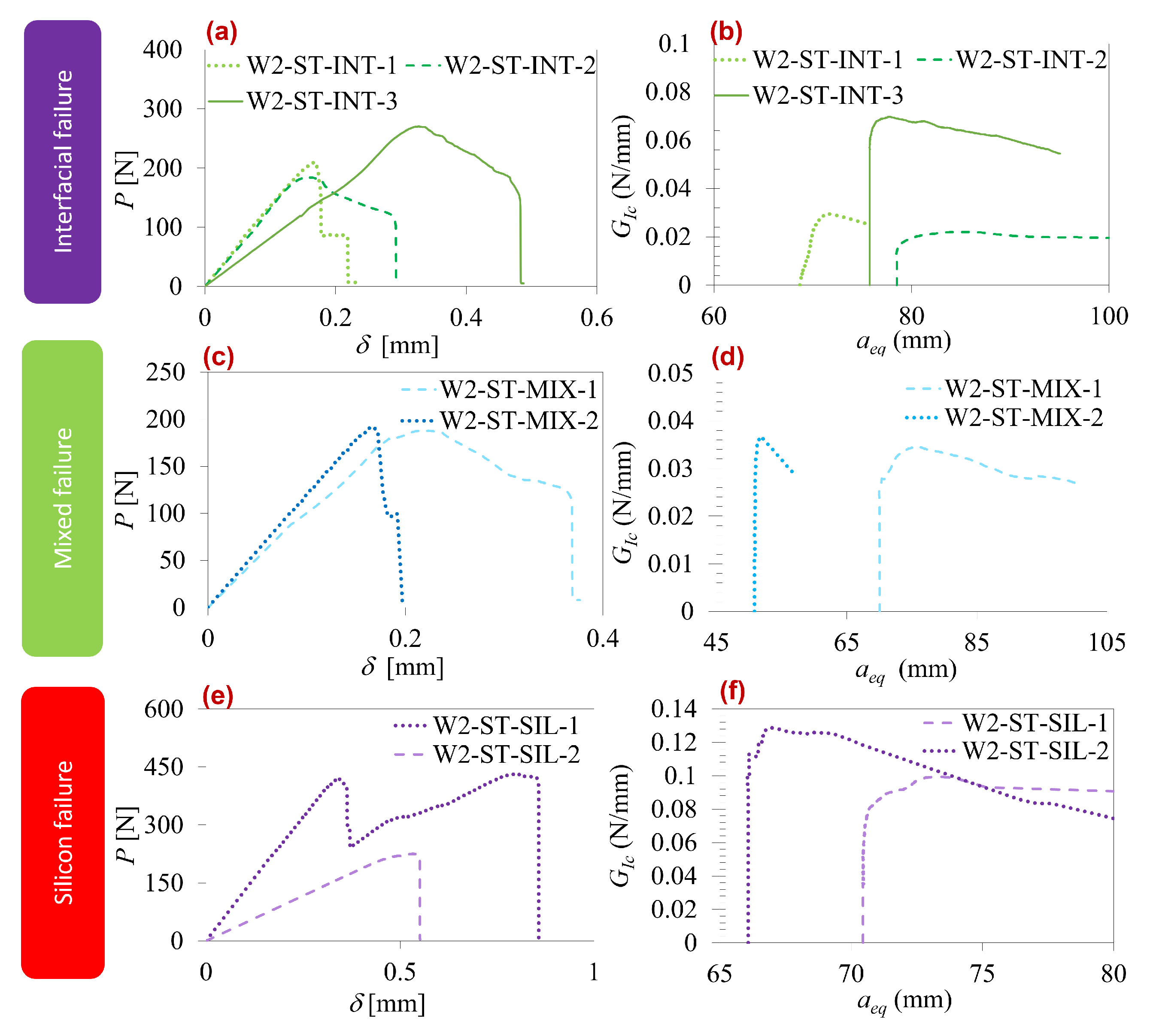
2.4.1. Quasi-Static Results
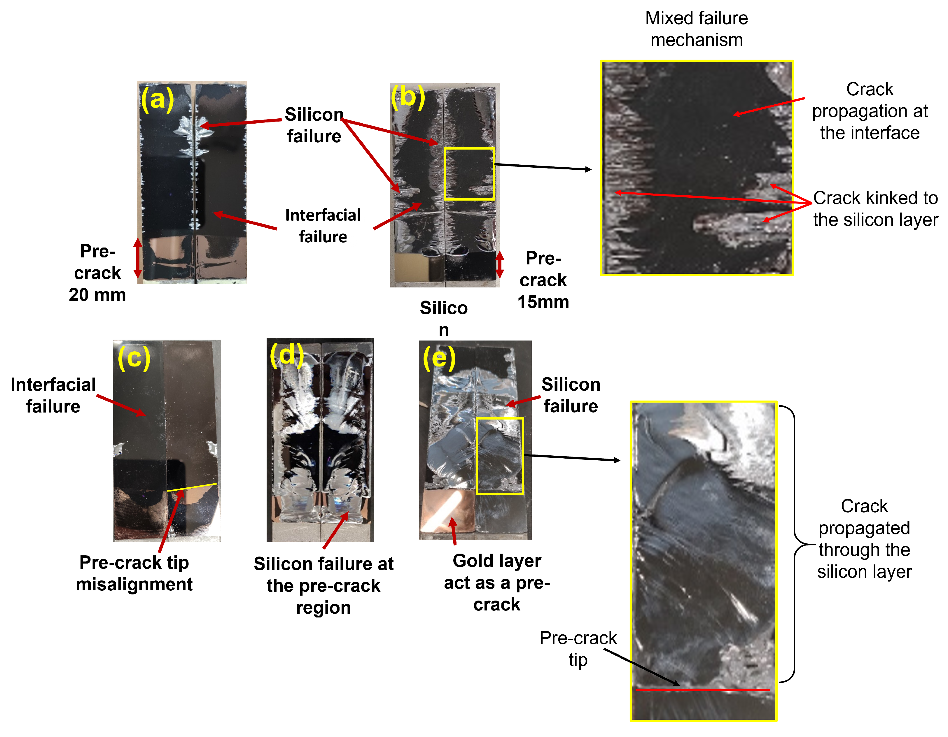
Failure Modes
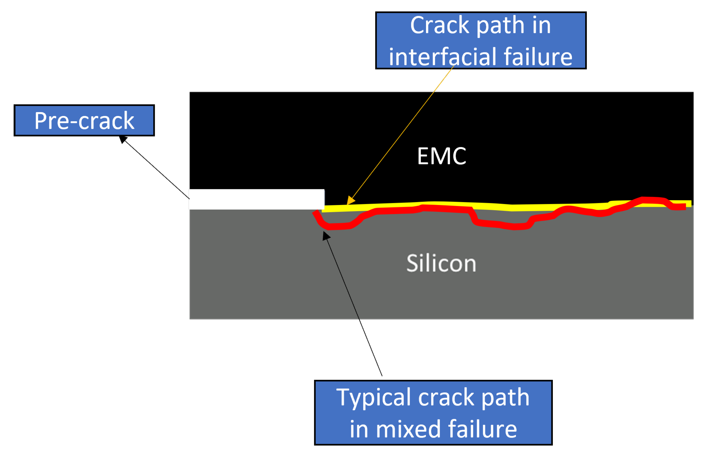
Fracture Analysis
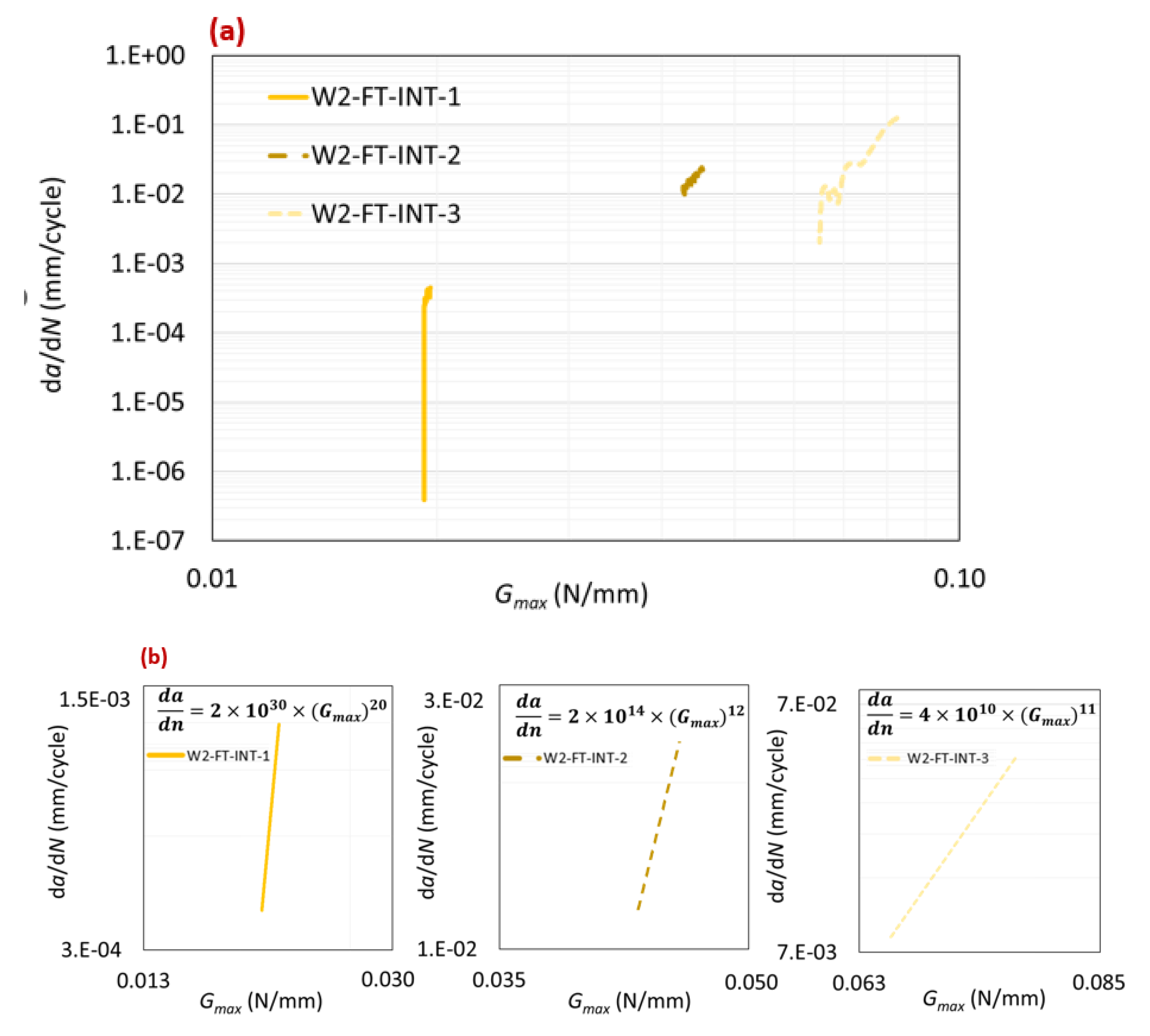
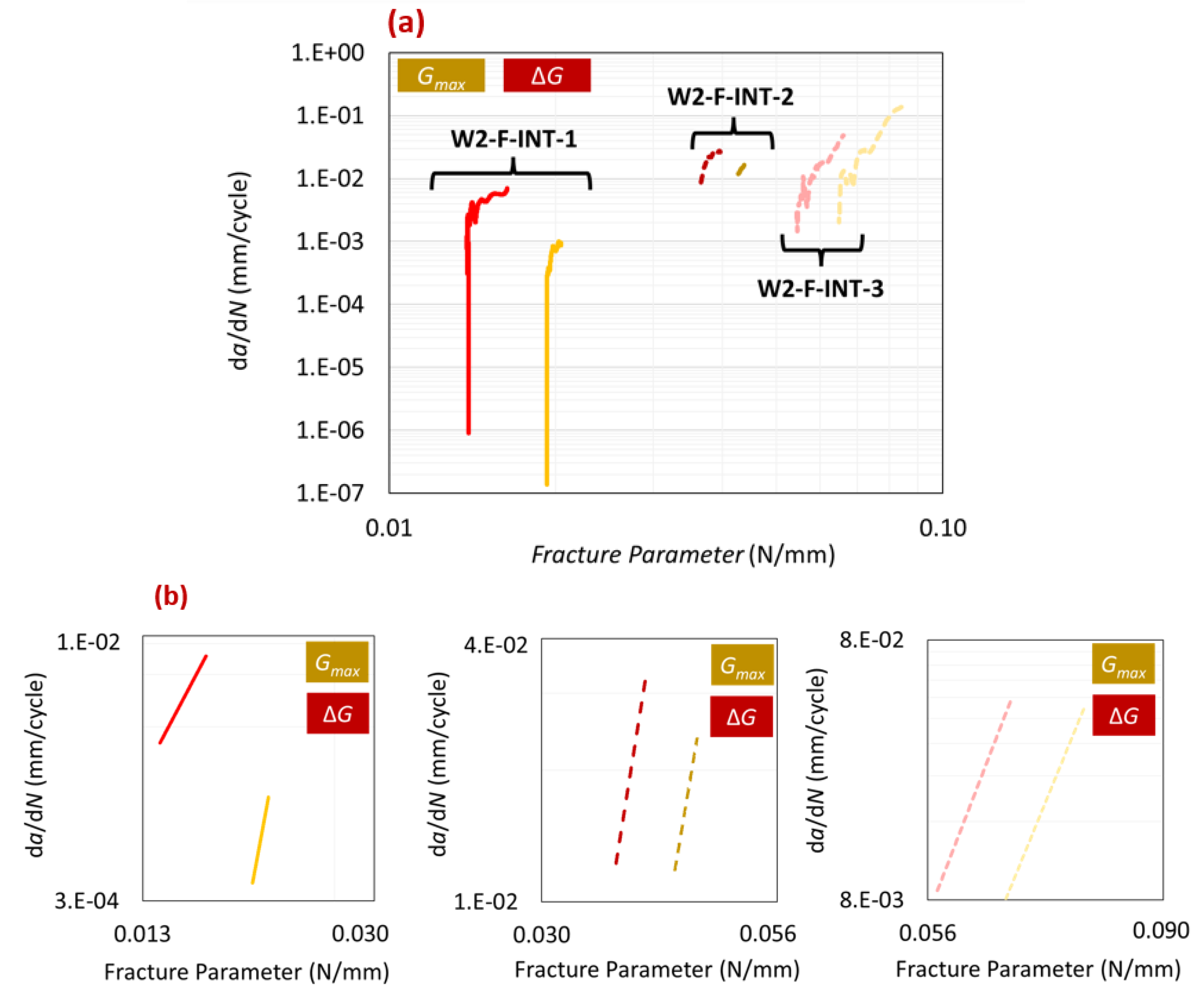
2.5. Fatigue Results
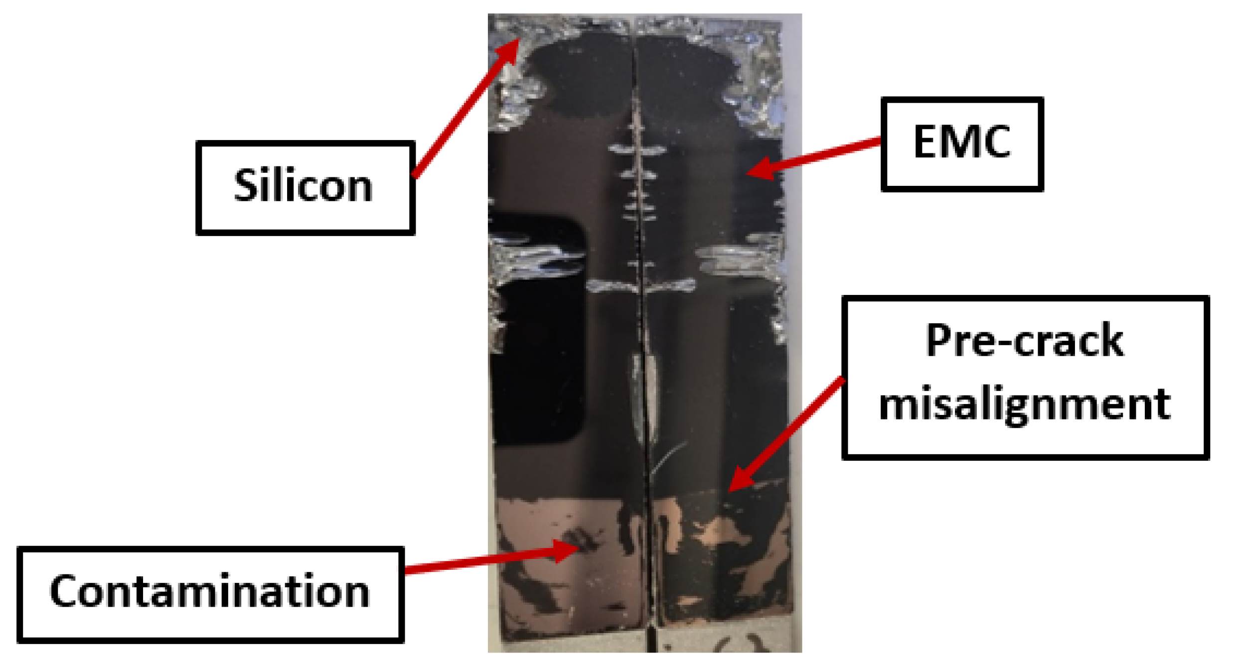
2.5.1. Failure Modes
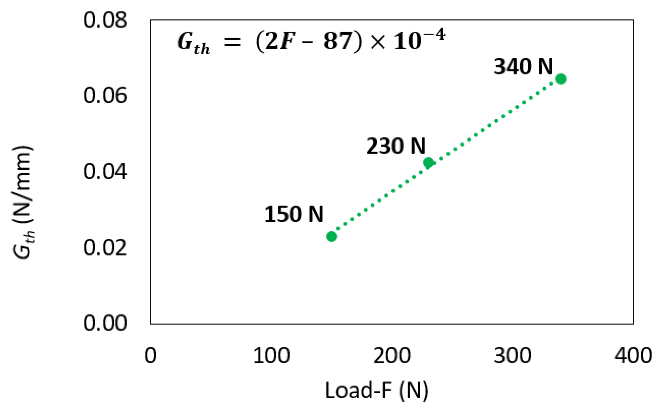
2.5.2. Fracture Analysis
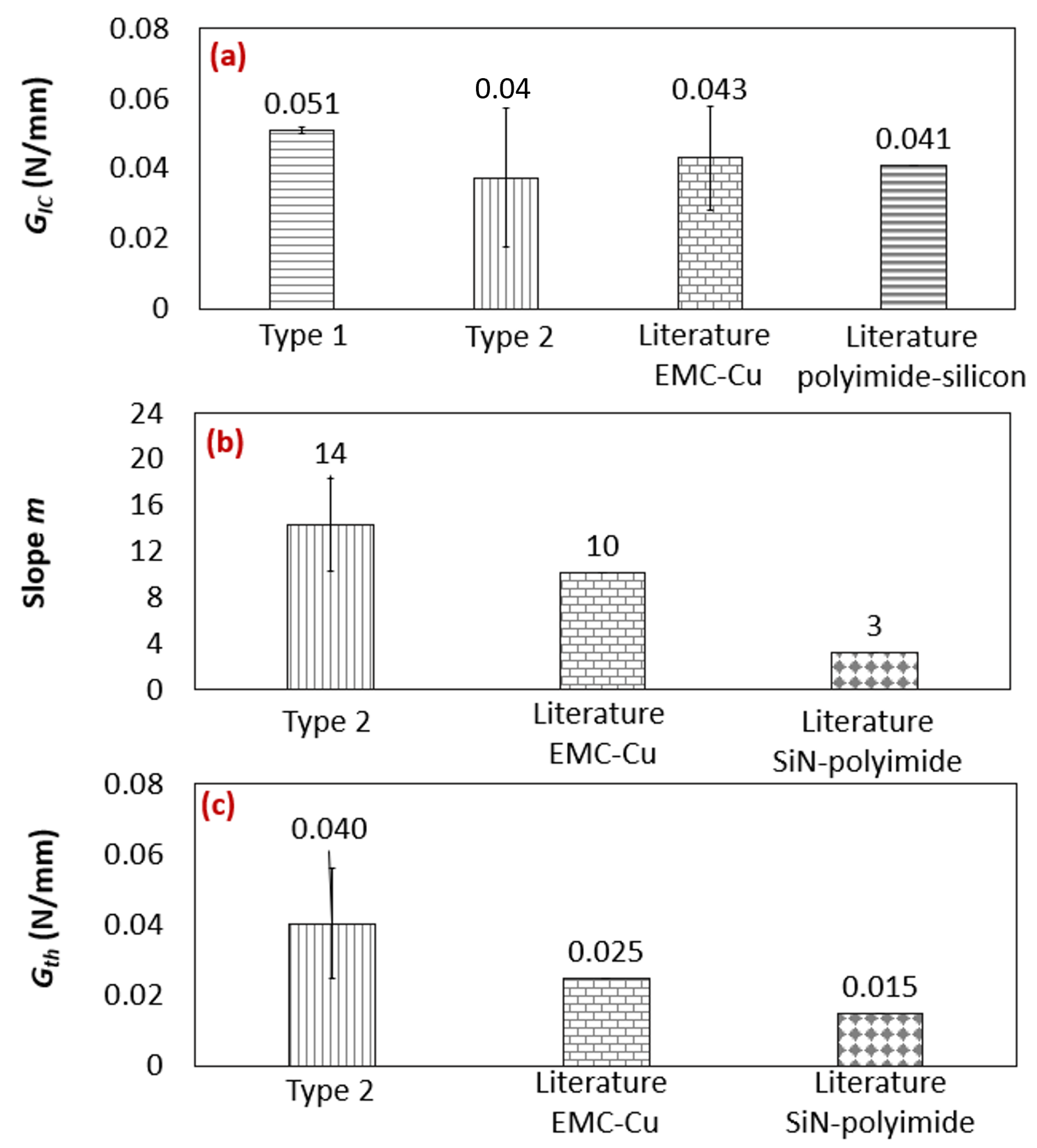
2.6. Comparison with the Literature
3. Conclusions
Author Contributions
Funding
Institutional Review Board Statement
Data Availability Statement
Acknowledgments
Conflicts of Interest
References
- Samet, D.S. Development of a Fatigue-Compatible Cohesive Zone Method for A Copper-Epoxy Molding Compound Bimaterial Interface. Ph.D. Thesis, Georgia Institute of Technology, Atlanta, GA, USA, 2018. [Google Scholar]
- Samet, D.; Rambhatla, V.T.; Kwatra, A.; Sitaraman, S.K. A fatigue crack propagation model with resistance curve effects for an epoxy/copper interface. Eng. Fract. Mech. 2017, 180, 60–72. [Google Scholar] [CrossRef]
- Rambhatla, V.T.; Sitaraman, S.K. Crowbar Loading-A New Test Technique to Characterize Interfacial Delamination. Eng. Fract. Mech. 2023, 282, 109144. [Google Scholar] [CrossRef]
- Calabretta, M.; Sitta, A.; Oliveri, S.M.; Sequenzia, G. Copper to resin adhesion characterization for power electronics application: Fracture toughness and cohesive zone analysis. Eng. Fract. Mech. 2022, 266, 108339. [Google Scholar] [CrossRef]
- Thijsse, J.; Van Driel, W.; Van Gils, M.; Van Der Sluis, O. Interfacial adhesion method for semiconductor applications covering the full mode mixity. In Proceedings of the EuroSime 2006—7th International Conference on Thermal, Mechanical and Multiphysics Simulation and Experiments in Micro-Electronics and Micro-Systems, Como, Italy, 24–26 April 2006; pp. 1–5. [Google Scholar]
- Yan, Y.; Huang, K.; Sumigawa, T.; Kitamura, T. Fracture criterion of mixed-mode crack propagation along the interface in nanoscale components. Eng. Fract. Mech. 2018, 193, 137–150. [Google Scholar] [CrossRef]
- Zhu, S.W.; Shih, C.P.; Chiu, T.C.; Shen, G. Delamination fracture characteristics for polyimide-related interfaces under fatigue loadings. In Proceedings of the 2010 5th International Microsystems Packaging Assembly and Circuits Technology Conference, Taipei, Taiwan, 20–22 October 2010; pp. 1–4. [Google Scholar]
- Schlottig, G. Reliability at the Chip Interfaces: Delaminating the Silicon Die From Molding Compound. Ph.D. Thesis, Delft University of Technology, Delft, The Netherlands, 2012. [Google Scholar]
- Wang, J.; Zou, D.; Lu, M.; Ren, W.; Liu, S. Evaluation of interfacial fracture toughness of a flip-chip package and a bimaterial system by a combined experimental and numerical method. Eng. Fract. Mech. 1999, 64, 781–797. [Google Scholar] [CrossRef]
- Mavinkurve, A.; Goumans, L.; Martens, J. Epoxy molding compounds for high temperature applications. In Proceedings of the 2013 Eurpoean Microelectronics Packaging Conference (EMPC), Grenoble, France, 9–12 September 2013; pp. 1–7. [Google Scholar]
- Masolin, A.; Bouchard, P.O.; Martini, R.; Bernacki, M. Thermo-mechanical and fracture properties in single-crystal silicon. J. Mater. Sci. 2013, 48, 979–988. [Google Scholar] [CrossRef]
- Gouzman, I.; Grossman, E.; Verker, R.; Atar, N.; Bolker, A.; Eliaz, N. Advances in polyimide-based materials for space applications. Adv. Mater. 2019, 31, 1807738. [Google Scholar] [CrossRef] [PubMed]
- Ehrhardt, J.; Klimmer, A.; Eisenmenger, J.; Müller, T.; Boyen, H.G.; Ziemann, P.; Biskupek, J.; Kaiser, U. Influence of ion induced amorphicity on the diffusion of gold into silicon. J. Appl. Phys. 2006, 100. [Google Scholar] [CrossRef]
- A Background to Silicon and Its Applications. Available online: https://www.azom.com/properties.aspx?ArticleID=599 (accessed on 5 December 2023).
- Silica—Silicon Dioxide (SiO2). Available online: https://www.azom.com/article.aspx?ArticleID=1114 (accessed on 5 December 2023).
- Da Silva, L.F.; Rodrigues, T.; Figueiredo, M.; De Moura, M.; Chousal, J. Effect of adhesive type and thickness on the lap shear strength. J. Adhes. 2006, 82, 1091–1115. [Google Scholar] [CrossRef]
- Neto, J.; Campilho, R.D.; Da Silva, L. Parametric study of adhesive joints with composites. Int. J. Adhes. Adhes. 2012, 37, 96–101. [Google Scholar] [CrossRef]
- Perez, M.; Akhavan-Safar, A.; Carbas, R.J.; Marques, E.A.; Wenig, S.; da Silva, L.F. Loading rate and temperature interaction effects on the mode I fracture response of a ductile polyurethane adhesive used in the automotive industry. Materials 2022, 15, 8948. [Google Scholar] [CrossRef] [PubMed]
- Rocha, A.; Akhavan-Safar, A.; Carbas, R.; Marques, E.; Goyal, R.; El-Zein, M.; Da Silva, L. Paris law relations for an epoxy-based adhesive. Proc. Inst. Mech. Eng. Part J. Mater. Des. Appl. 2020, 234, 291–299. [Google Scholar] [CrossRef]
- Erpolat, S.; Ashcroft, I.; Crocombe, A.; Abdel-Wahab, M. Fatigue crack growth acceleration due to intermittent overstressing in adhesively bonded CFRP joints. Compos. Part A Appl. Sci. Manuf. 2004, 35, 1175–1183. [Google Scholar] [CrossRef]
- Krieger, W.E.; Raghavan, S.; Sitaraman, S.K. Experiments for obtaining cohesive-zone parameters for copper-mold compound interfacial delamination. IEEE Trans. Compon. Packag. Manuf. Technol. 2016, 6, 1389–1398. [Google Scholar] [CrossRef]


| Materials | Ultimate Tensile Strength (MPa) | Poisson’s Ratio | Young’s Modulus (GPa) |
|---|---|---|---|
| Silicon | 165 | 0.28 | 112 |
| EMC | 90 | 0.38 | 2.36 |
| PM300 | 1020 | 0.33 | 205 |
| Polyimide | 300 | 0.4 | 3.73 |
| Silicon oxide | 45 | 0.17 | 73 |
| Young´s modulus (GPa) | 4.59 ± 0.81 |
| Tensile yield strength (MPa) | 36.49 ± 2.47 |
| Ultimate tensile strength (MPa) | 41.01 ± 7.28 |
| Tensile failure strain (%) | 7.80 ± 0.70 |
| Poisson’s ratio | 0.35 |
| Test Code | Interface Type | Failure Mechanism | Max Load (N) | Max Displacement (mm) | (N/mm) |
|---|---|---|---|---|---|
| W1-ST-INT1 | 1 | Interfacial | 292 | 0.456 | 0.052 |
| W1-ST-INT2 | 260 | 0.454 | 0.050 | ||
| W2-ST-INT-1 | 2 | 210 | 0.219 | 0.028 | |
| W2-ST-INT-2 | 184 | 0.292 | 0.019 | ||
| W2-ST-INT-3 | 270 | 0.483 | 0.065 | ||
| W1-ST-MIX-1 | 1 | Mixed | 574 | 0.653 | 0.155 |
| W1-ST-MIX-2 | 321 | 0.561 | 0.065 | ||
| W1-ST-MIX-3 | 317 | 0.611 | 0.075 | ||
| W1-ST-MIX-4 | 371 | 0.626 | 0.045 | ||
| W2-ST-MIX-1 | 2 | 188 | 0.369 | 0.03 | |
| W2-ST-MIX-2 | 194 | 0.192 | 0.035 | ||
| W2-ST-SIL-1 | 2 | Silicon | 431 | 0.857 | 0.125 |
| W2-ST-SIL-2 | 225 | 0.551 | 0.095 |
| Test Code | Interface Type | Failure Mechanism | Fatigue Load (N) | FCG Rate (mm) | (N/mm) |
|---|---|---|---|---|---|
| W2-FT-INT-1 | Two | Interfacial | 150 | 20 | 0.0192 |
| W2-FT-INT-2 | 230 | 11 | 0.0427 | ||
| W2-FT-INT-3 | 340 | 11 | 0.0645 |
| Fracture Parameter | Test Code | Slope, m | (N/mm) |
|---|---|---|---|
| W2-FT-INT-1 | 20 | 0.0192 | |
| W2-FT-INT-2 | 11 | 0.0427 | |
| W2-FT-INT-3 | 11 | 0.0645 | |
| W2-FT-INT-1 | 7 | 0.0138 | |
| W2-FT-INT-2 | 12 | 0.0367 | |
| W2-FT-INT-3 | 11 | 0.0546 |
Disclaimer/Publisher’s Note: The statements, opinions and data contained in all publications are solely those of the individual author(s) and contributor(s) and not of MDPI and/or the editor(s). MDPI and/or the editor(s) disclaim responsibility for any injury to people or property resulting from any ideas, methods, instructions or products referred to in the content. |
© 2024 by the authors. Licensee MDPI, Basel, Switzerland. This article is an open access article distributed under the terms and conditions of the Creative Commons Attribution (CC BY) license (https://creativecommons.org/licenses/by/4.0/).
Share and Cite
Morais, P.; Akhavan-Safar, A.; Carbas, R.J.C.; Marques, E.A.S.; Karunamurthy, B.; da Silva, L.F.M. Mode I Fatigue and Fracture Assessment of Polyimide–Epoxy and Silicon–Epoxy Interfaces in Chip-Package Components. Polymers 2024, 16, 463. https://doi.org/10.3390/polym16040463
Morais P, Akhavan-Safar A, Carbas RJC, Marques EAS, Karunamurthy B, da Silva LFM. Mode I Fatigue and Fracture Assessment of Polyimide–Epoxy and Silicon–Epoxy Interfaces in Chip-Package Components. Polymers. 2024; 16(4):463. https://doi.org/10.3390/polym16040463
Chicago/Turabian StyleMorais, Pedro, Alireza Akhavan-Safar, Ricardo J. C. Carbas, Eduardo A. S. Marques, Bala Karunamurthy, and Lucas F. M. da Silva. 2024. "Mode I Fatigue and Fracture Assessment of Polyimide–Epoxy and Silicon–Epoxy Interfaces in Chip-Package Components" Polymers 16, no. 4: 463. https://doi.org/10.3390/polym16040463