Article

Investigating the Device Performance Variation of a Buried Locally Gated Al/Al2O3 Graphene Field-Effect Transistor Process

by
Tzu-Jung Huang
1,
Adheesh Ankolekar
2,
Anibal Pacheco-Sanchez
3 and
Ivan Puchades
2,*
1
Department of Microsystems Engineering, Rochester Institute of Technology, Rochester, NY 14623, USA
2
Department of Electrical and Microelectronic Engineering, Rochester Institute of Technology, Rochester, NY 14623, USA
3
Departament d’Enginyeria Electrònica, Escola d’Enginyeria, Universitat Autònoma de Barcelona, 08193 Bellaterra, Spain
*
Author to whom correspondence should be addressed.
Appl. Sci. 2023, 13(12), 7201; https://doi.org/10.3390/app13127201
Submission received: 21 May 2023 / Revised: 10 June 2023 / Accepted: 12 June 2023 / Published: 16 June 2023
(This article belongs to the Special Issue Laser-Induced Graphene and Its Applications in Flexible Electronics)

Abstract

:
In this study, a process is developed for the fabrication of buried top-gated graphene transistors with Al2O3 as a gate dielectric, yielding devices that can be suitable for not only flexible electronics but also laser-induced graphene (LIG)-based technology implementations. A new processing option is presented with the use of tetraethyl-orthosilicate (TEOS) as an etch stop for contact via etching of Al2O3. Buried locally gated Al/Al2O3 graphene field-effect transistors (GFETs) are fabricated with Dirac points as low as 4 V, with a metal-to-graphene contact resistance as low as ∼1.7 kΩ·µm, and an average hole mobility of 457.97 cm2/V·s with a non-uniformity of 93%. Large device variation and non-uniformity in electrical performance are not uncommon for graphene-based devices, as process-induced defects play a major role in such variation. AFM, SEM, Raman spectroscopy, and model fitting indicated that the rough Al/Al2O3 surface was the main factor for the observed device variation. AFM analysis indicated a graphene surface roughness Ra of 16.19 nm on top of the buried Al/Al2O3 gate in contrast to a Ra of 4.06 nm over Al2O3/SiO2. The results presented indicate the need to reduce device variability and non-uniformity by improving transfer methods, as well as the use of smoother surfaces and compatible materials. The presented analyses provide a framework with which other researchers can analyze and correlate device variation and non-uniformities while methods to reduce variability are investigated.

1. Introduction

Graphene is a low-dimensionality material which offers several advantages as an emerging electronic material in terms of high mobility (200,000 cm2/V·s) [1], high carrier concentration [2], high tensile strength (125 GPa) [3], and high thermal conductivity (∼4000 W·m−1·K−1) [4]. In addition, graphene is inherently flexible, transparent, and chemically inert. Moreover, it has been adopted in several applications, such as bendable display technology, electrochemical energy storage devices, metal corrosion inhibitors, and signal processing and signal modulation applications [5,6,7,8]. Graphene does not have a bandgap; as such, it has found limited applications as a logic gate [9,10,11,12], although attempts have been made to form a bandgap with a bilayer graphene (BLG) structure [13]. On the other hand, due to its high mobility, there have been significant efforts toward the fabrication of graphene field-effect transistors (GFETs) for their application in high-frequency amplifiers, modulators, and resonators [14,15,16]. In addition, due to the sensitivity of graphene to physical and chemical stimuli, there are numerous reports of graphene-based physical and chemical sensors [17,18,19,20].
There are several reported fabrication methods of graphene-based devices [21,22,23,24,25]. The choice of the fabrication method comes down to the final application and the required performance, as well as the available resources. High-performing GFETs typically consist of nanometer-length channels and reduced S/D capacitance techniques [26], and reported studies have achieved an extrinsic cutoff frequency (fT) of 34 GHz, as well as an extrinsic maximum oscillation frequency (fmax) of 37 GHz with gate lengths <350 nm fabricated via electron beam lithography [26]. Gate electrodes for these devices are generally fabricated with a top [27], buried [28], or trench-filled (damascene process) [29] structure. Gate dielectric materials of ultrathin AlOx (naturally grown or ALD), hBN (transferred), and other high-k materials are used in order to maximize the performance of these devices [30,31,32]. Additionally, the substrate that creates an interface with graphene is carefully selected to minimize adverse effects [33]. Published reports have shown that, even though high-volume production of such transistors results in a reasonably high number of working devices (high yield), the device-to-device variation and non-uniformity of their electrical characteristics remain quite high [34,35,36,37,38]. Non-uniformity (NU) is a value of device variation and can be calculated as NU = (max − min)/average. The value of non-uniformity can be used as a figure of merit of variability when not enough data exists to obtain a statistical meaningful normal distribution. For example, Smith et al. reported the fabrication of 4500 top-gated GFETs with a yield of 75%, a median Dirac point of 4 V, and mobility of 40 cm2/V·s, but non-uniformity of 150% and 300% [34]. The observed device variation was explained by graphene defects during transfer, the strain of graphene, transfer polymer residue, and interface substrate effects [34,35,36,39].
In contrast, in the design and fabrication of graphene-based THz resonators for communication systems and chemical/physical sensors, the dimensions of the proposed devices are in the micrometer range (1–100 s·µm) to meet the required performance of the application. THz resonators have been proposed through the hydrodynamic electron fluid concept applied to the Dyakonov and Shur (DS) instability [40,41,42]. THz radiation has been predicted in structures with high electron density and high-carrier-mobility materials with certain boundary conditions. The dimensions of these THz resonators are designed to match the targeted wavelengths at resonance [43]. Likewise, the design and fabrication of graphene-based chemical and physical sensors require devices with graphene dimensions in the micrometer range [44] to provide enough sensing area [17]. While sensors do not require large mobility, they do require repeatability between devices for robust and consistent signals [18]. In both cases, due to the larger relative dimensions of the graphene channel (1–100 µm), it is expected that these large-area devices will be more susceptible to material variations that have been observed and reported in the graphene transfer and/or synthesis process [24,34]. For example, Lerner et al. reported the fabrication and testing of >12,000 global back gate GFET sensors with an average Dirac point and hole mobility of 22.5 V and 4959 cm2/V·s, but non-uniformities of 88% and 200% [36].
The fabrication methods for larger-area sensor devices require that graphene be exposed to the stimuli; as such, a back-gated or buried-gate process is preferred. A buried-gate process not only provides the extra advantage and flexibility of being able to access each sensor individually on the same substrate but also assists in the decrease in parasitic source-to-gate and source-to-drain capacitance in comparison to global back gates. In a buried-gate process, aluminum can be used as the gate material as it is readily available, is inexpensive, and can be deposited in multiple ways (sputter, thermal, and e-beam evaporation). In addition, the gate dielectric does not need to be ultrathin, as higher bias levels may be required to obtain more robust signals [24]. As such, atomic layer-deposited (ALD) Al2O3 is often used as a dielectric as it generally provides lower interface traps than other CVD-based dielectrics, a lower Dirac point, and more repeatable results [24]. The integration of a buried aluminum gate with an ALD Al2O3 dielectric presents the challenge of etch compatibility when accessing the buried aluminum gate electrode. Although some have reported that the top Al2O3 can be simply scratched away during testing [45], the general approach is to apply the Al2O3 layer in a fluorine-based plasma etch, as it has excellent selectivity to the underlying aluminum [46,47], a wet chemical etch in BOE, or a diluted resist developer [26,48]. As a downside, the fluorinated plasma etch of Al2O3 is slow with only CF4 gas at an etch rate of 4.5 nm/min [47]. The inclusion of O2 in etch gas can increase the etch rate [49] but it may become challenging to complete with a standard photoresist mask as the etch selectivity to any organic materials decreases.
There are several methods to synthesize graphene [50]. Among these, chemical vapor deposition (CVD) on a copper substrate results in large-area and high-quality single-layer graphene [51]. This CVD-grown graphene on Cu can then be transferred onto any needed substrate through wet, dry, or other alternative methods, thus providing process flexibility [52]. Another synthesis method, laser-induced graphene (LIG), has recently attracted extensive interest for chemical and biological sensors [19,50,51]. LIG can be integrated with both resistive-based [19] and field-effect transistor-based devices [53], where the graphene channel is exposed for sensing applications. One of the great advantages of LIG synthesis is that it completely eliminates the need for a graphene transfer process. Graphene formed directly on a polyimide (PI) [54] or any cross-linked hybrid lignocellulose [55] substrate via a laser writer offers the ability to achieve a minimum spatial resolution of 12 µm and has been reported by Stanford et al. [56]. The synthesized LIG consists of multilayer graphene with a high porosity characteristic that provides a much larger surface area when compared to monolayer graphene, which is favorable for chemical sensing applications. As with other graphene-based devices, the reported variation in sensitivity and performance remains a significant challenge of this method that must be investigated. For instance, Tour et al. reported the fabrication and test of LIG gas sensors with an average gas sensitivity (ΔR/RHe) of 2.99 with a non-uniformity of 206% [19].
There is a need to understand device variability of micrometer-size GFETs, as well as the sources of variation. The work presented in this paper focuses on a large area process for devices with a 1–10 µm channel length and a buried aluminum local gate electrode aimed at applications such as graphene-based THz modulators and sensors. An alternative method to integrate an ALD Al2O3 gate dielectric using chlorine chemistry and an etch stop is presented. A large number of fabricated devices are electrically tested in order to analyze device variability in terms of electrical performance. In addition, SEM, Raman spectroscopy, and AFM are used to investigate the sources of variation as they relate to the process and electrical results. Lastly, the conclusions provide insights into the sources of variation and possible solutions that can be used to improve variability.

2. Materials and Methods

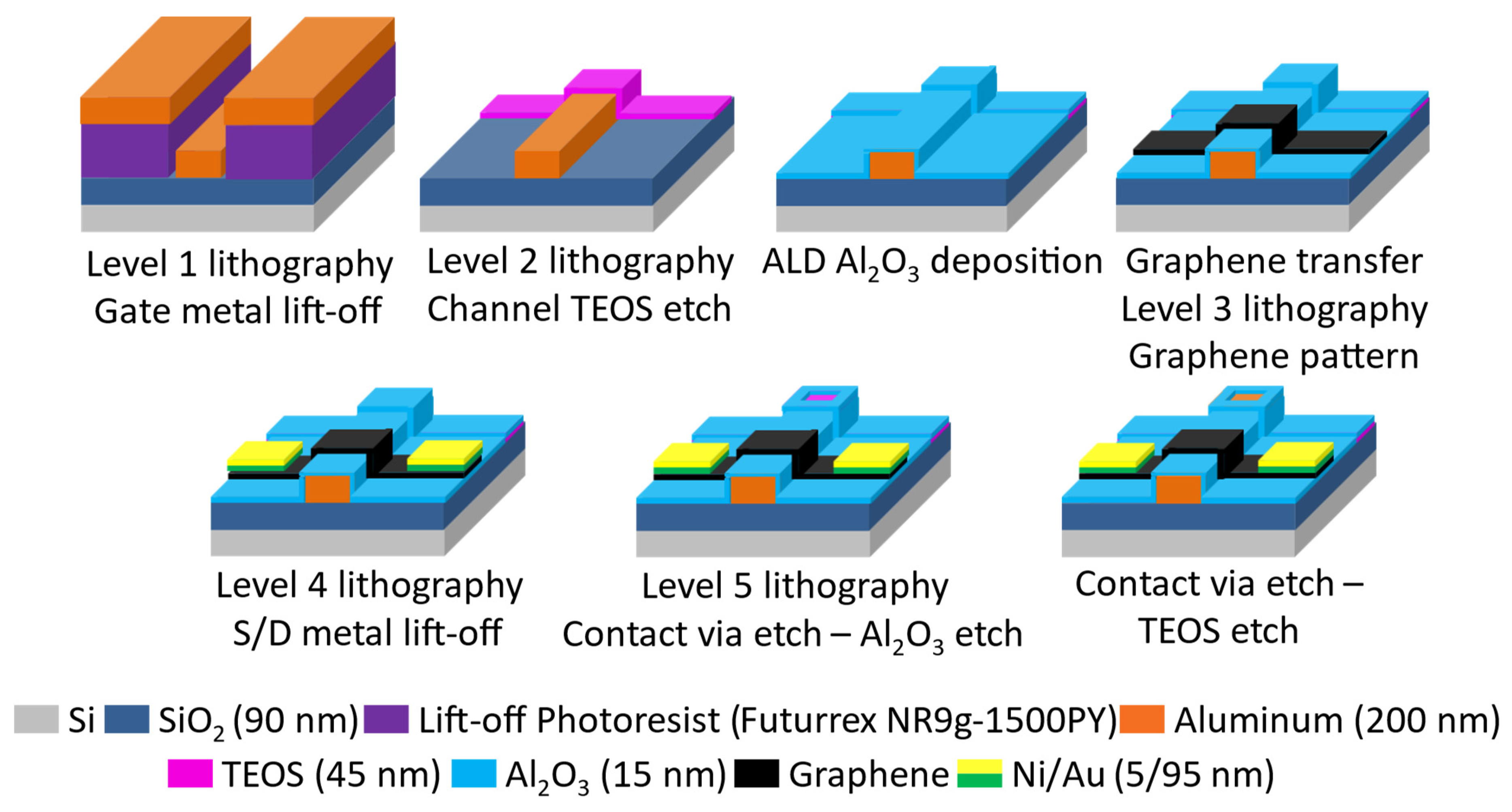
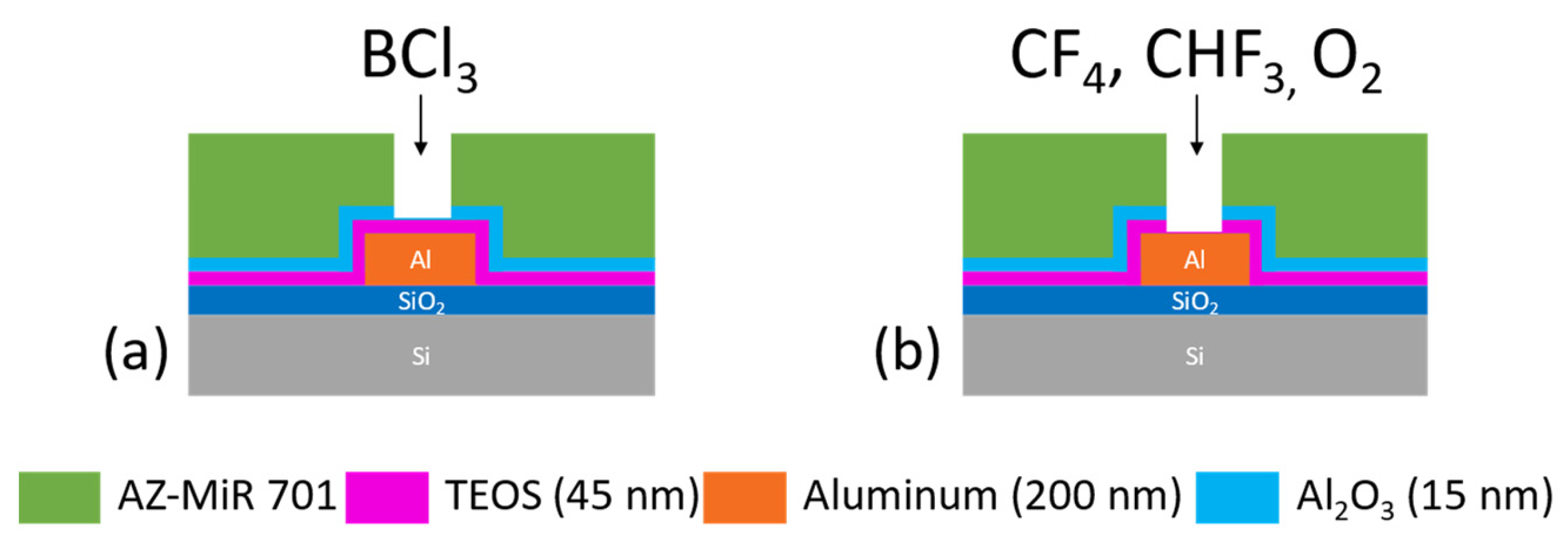
2.1. Device Fabrication

Shown in Figure 1 is a step-by-step process diagram of the device fabrication. The devices presented in this work were processed on a 6″ Si wafer to demonstrate the scalability of the proposed process. Alignment marks were first etched into n-type silicon wafers (100) for the ASML PAS 5500 i-line stepper, where all standard and lift-off lithography steps were performed thereafter. Following a standard RCA clean, 90 nm of SiO2 was thermally grown at 1000 °C. Next, 200 nm of aluminum was thermally evaporated and patterned through a lift-off lithography process to serve as a gate electrode. The evaporation was conducted using a CVC thermal evaporator with 99.95% purity aluminum pellets. A 45 nm layer of PECVD TEOS was then deposited directly on top of the patterned gate electrodes to serve as an alumina etch stop when opening up contact vias. TEOS was patterned and etched away in a Trion Phantom III RIE with 60 sccm of CF4, CHF3 and 8 sccm of O2 with RF power of 200 W to expose the aluminum gate electrode in the active area. Next, 15 nm of Al2O3 was deposited using an Ultratech S200 G2 Savannah atomic layer deposition (ALD) system with 150 cycles. High-quality CVD-grown monolayer graphene on copper foil (6″ × 6″) was commercially purchased from Graphenea, Inc. An area of 3″ by 2″ was cut out and transferred onto the surface of the wafer with a double PMMA-assisted process, described in detail in the next section. Graphene was then patterned through standard lithography by oxygen plasma via Trion Phantom III RIE for 60 s. The resist was removed by acetone soak and rinsed with DI water. Ni and Au (5 and 95 nm, respectively) were thermally evaporated sequentially and patterned for source and drain contacts via a lift-off process. Finally, the wafers were coated with photoresist, and contact vias were patterned and etched away to expose the aluminum gate contact pads. This was performed in a two-step process, first etching the Al2O3 in the Plasmatherm ICP Etcher with chlorine-based chemistry and then the etch-stop TEOS layer in the Trion Phantom III with fluorine-based chemistry (details in Section 3). Individual chips containing several graphene FETs and test structures were cut into 1 cm by 1 cm chips using an ADT Dicing Saw 7120 prior to removing the photoresist protecting the graphene in the previous step.

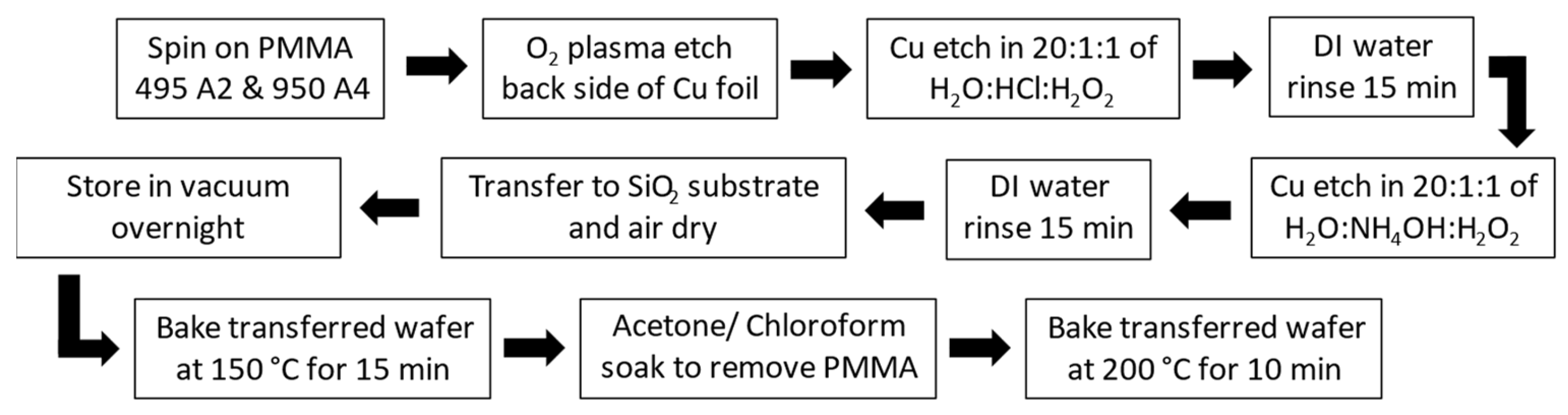
2.2. Graphene Transfer

High-quality CVD-grown monolayer graphene on copper foil was commercially purchased from Graphenea, Inc., Cambridge, MA, USA. [57]. An area of 3″ by 2″ was carefully cut out, and a modified PMMA-assisted graphene transfer, depicted in Figure 2, was used to transfer the monolayer graphene to the destination substrate [12,13]. Graphene on copper foil was taped onto a carrier wafer using Kapton tape. Two different PMMA solvents, 495 A2 and 950 A4 manufactured and purchased from Kayaku Advanced Materials, were used to compensate the stress of the stack of hard-baked polymer. The spin speeds for both PMMA 495 A2 and 950 A4 were kept at 1000 rpm for 30 s, each with a goal of obtaining a thicker coat (0.6 µm thickness in comparison to 0.25 µm at a 3000 rpm spin speed). PMMA was used to prevent the polymer/graphene stack from folding, warping, or ripping during transfer steps. The transfer process also consisted of baking the PMMA/graphene/copper stack on a hotplate at 200 °C for 2 min after each coat. The graphene was stored under vacuum overnight as reported from Langston et al. for a better adhesion of graphene to its substrate and for PMMA removal [58]. The PMMA was then removed by soaking the transferred wafer in an acetone bath at room temperature overnight, followed by baking the transferred sample stack on a hotplate at 200 °C for 10 min.

2.3. Test Methods

Electrical testing was conducted with a semi-automated RK probe card station, an HP-4156 parameter analyzer, and a manual SUSS electrical testing station with an HP-4145B parameter analyzer. Working devices were mapped out over 100 devices on the fabricated wafer across two dozen dies. Experimental data were collected for IDVG sweep and hysteresis tests with and without a pulse. Pulsed measurements were operated in a manner such that, after each applied VGS bias, a constant voltage was applied with the purpose of removing trap charges.
Raman spectroscopy was carried out with the JY Horiba Labram-HR Raman spectroscope for further analysis on the quality of post-processing transferred graphene at multiple interest points within the active device area. A red 633 nm laser was used for the spectroscopy measurement with a measurement accumulation time of 30 s per data point.
Contact resistance estimations were obtained using a well-known total resistance model of GFETs presented elsewhere [59]. The goal of the estimation of contact resistance is to understand the key factor of device performance determinants. This method provides an immediate and straightforward approximation of the device performance, as well as eliminates the need for building and designing transfer length measurement structures (TLMs).

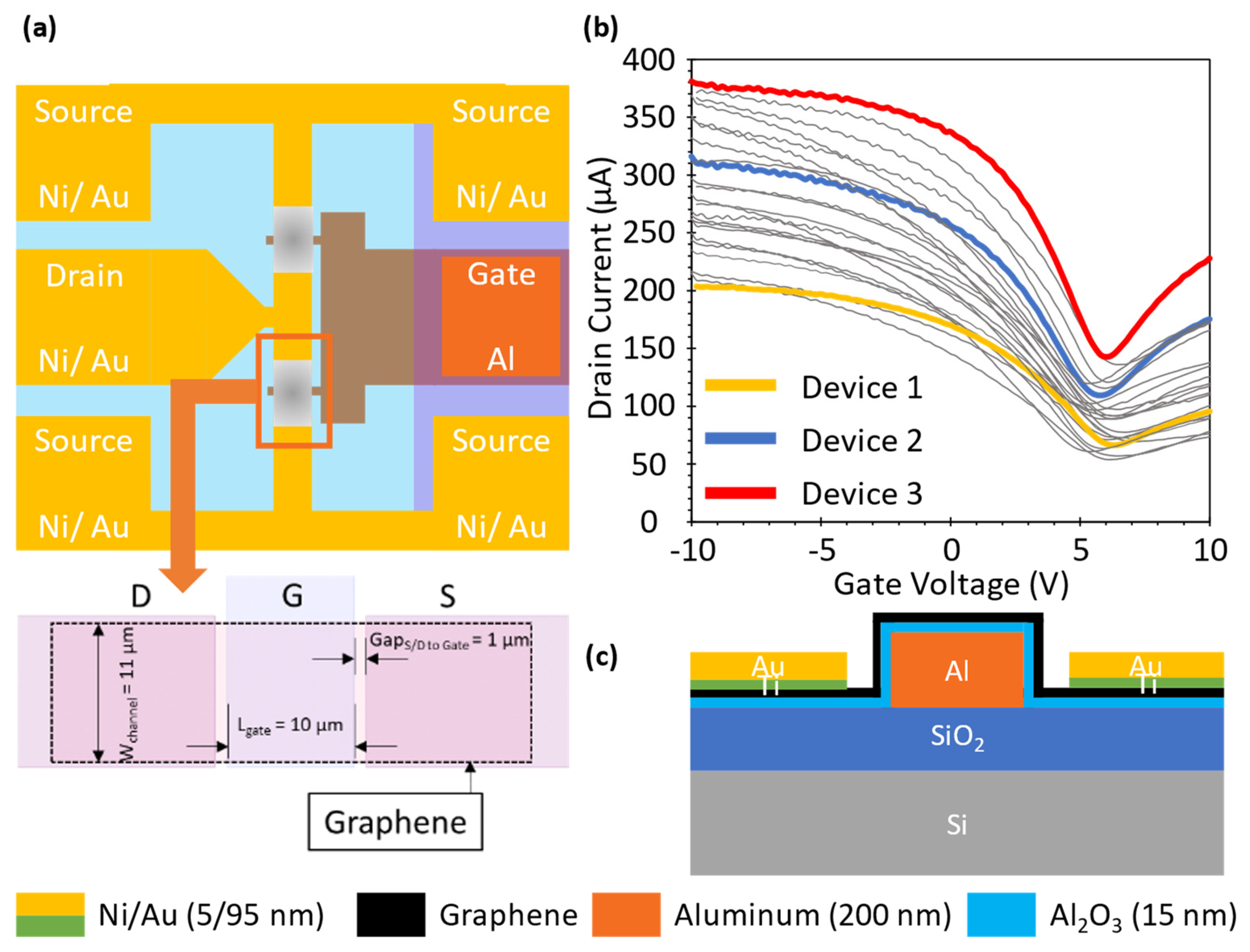
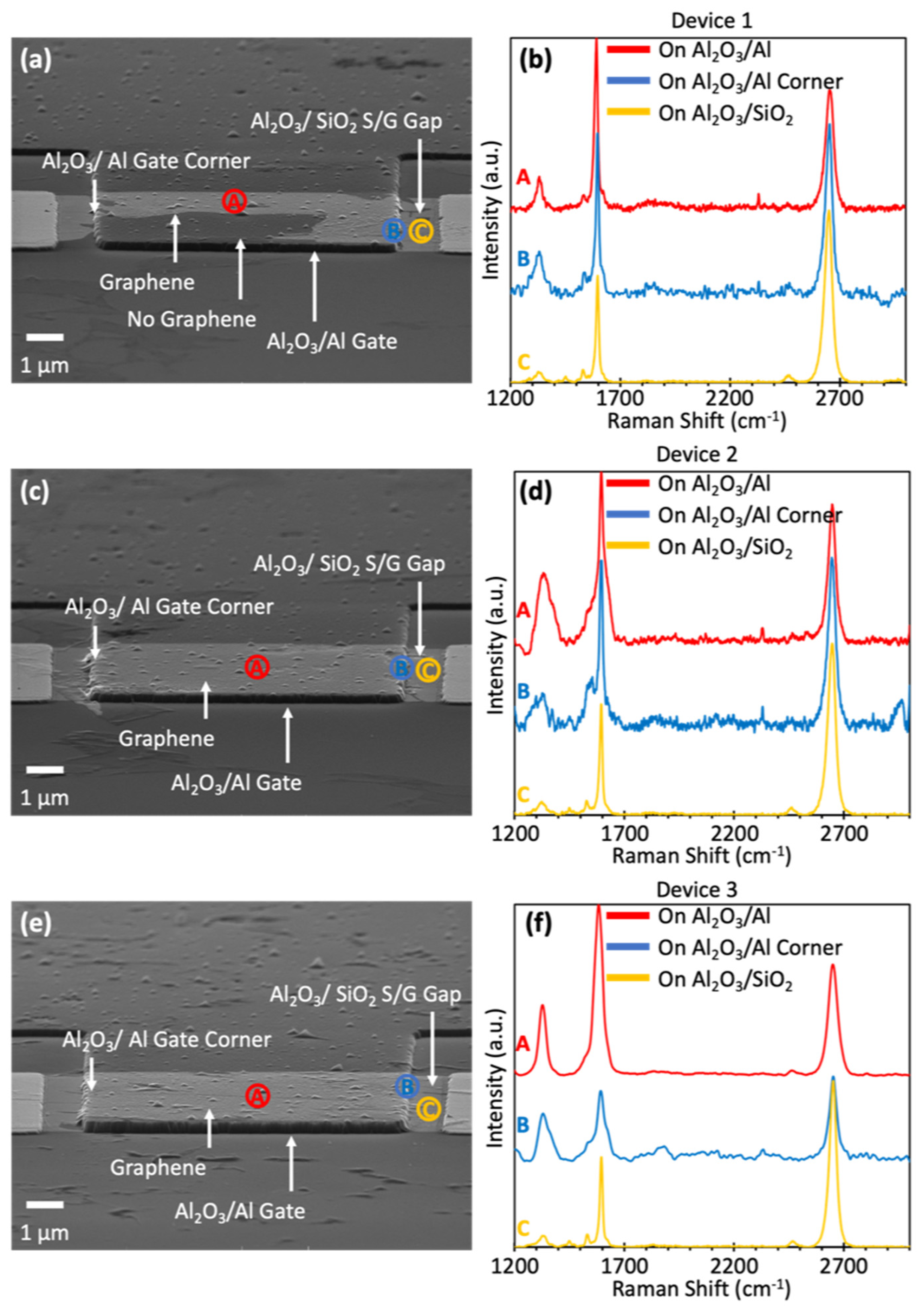
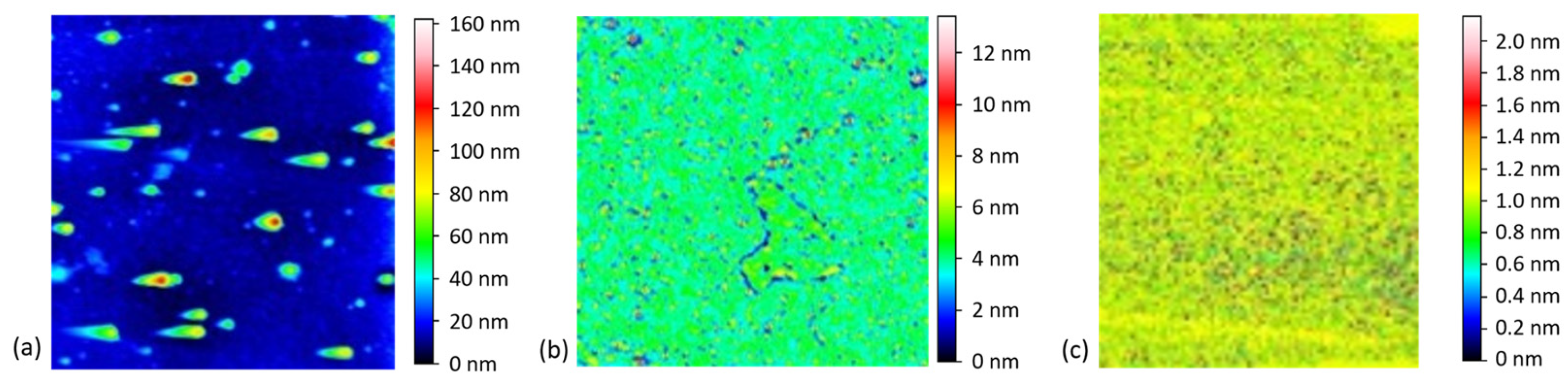
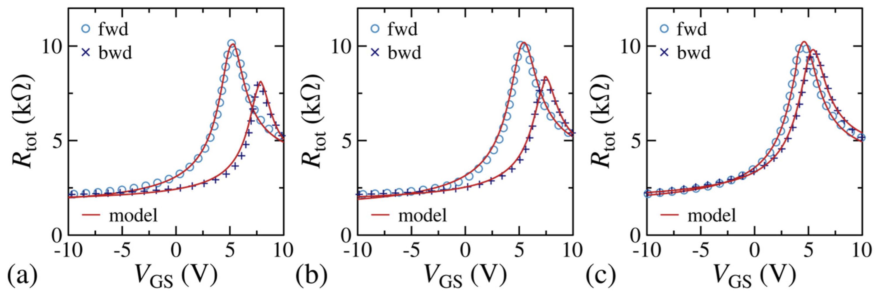
3. Results and Discussion

As presented in Section 1, the integration of a buried aluminum gate with an ALD Al2O3 dielectric presents the challenge of etch compatibility when accessing the buried Al gate electrode. Although Al2O3 can be etched in a fluorine-based chemistry, with very high selectivity to Al, this etch is slow and requires nonstandard lithography, such as the use of a hard mask or a thicker photoresist. A selective method to etch the Al2O3 gate over the buried Al gate electrode using standard lithography has been developed and is shown in Figure 3. The proposed method includes a thin etch-stop TEOS layer between the Al and the Al2O3. This TEOS layer is 45 nm thick and deposited after the Al gate has been patterned. After deposition, the TEOS is patterned and etched in a fluorine-based dry chemistry as to only remain over the gate electrode contact locations away from the active channel area of the GFET, as shown in Figure 1. A 15 nm Al2O3 gate dielectric is then deposited via ALD and remains on the entire wafer. The graphene is then transferred and patterned, and the metal contacts are deposited and patterned, as described in Section 2. Finally, the contacts must also be patterned and etched to access the Al bottom gate. This is accomplished via a two-step etch process as shown in Figure 3a,b. The contact vias are patterned using conventional lithography with a 1 µm AZ-MiR 701 positive photoresist. The Al2O3 is then etched in the Plasmatherm ICP Etcher with 30 sccm of BCl3 for 23 s under a chamber pressure of 4 mTorr and 500 W of ICP source along with a 50 W RF bias where the high-selectivity to TEOS makes this layer act as an etch stop, as shown in Figure 3a. This BCl3 etch has an etch rate of 40 nm/min and allows the process to complete with the photoresist still remaining for the next step. The etch-stop TEOS layer is removed in the Trion Phantom III with 60 sccm of CF4, 70 sccm of CHF3, and 6 sccm of O2 for 60 s under 130 mTorr chamber pressure and 200 W of RF power as shown in Figure 3b, thereby exposing the Al gate contact.
Moreover, the proposed process may also be applicable to other etch materials for similar device structures to this work. Other published studies have demonstrated the use of other high-k atomic layer deposited materials such as HfO2 and TiO2 [29,60] for graphene or 2D material-based devices. While most high-k ALD dielectric materials can be etched with chlorine-based gas chemistries, the proposed etch process provides great value with minimum process optimization, and it can be easily adapted for a wide variety of device structures.
A schematic top view of the tested GFETs is shown in Figure 4a indicating the gate length (Lgate), width (Wchannel), and source/drain-to-gate gap (GapS/D to Gate). Although the fabricated devices are designed as dual-gated transistors, only one gate was tested at a time. Presented in Figure 4b are the IDS–VGS curves for 24 devices with identical device footprints with a channel width of 11 µm, a gate length of 12 µm, and a 1 µm source/drain-to-gate gap. The drain current levels range between 200 and 400 µA with a Dirac voltage between 5 and 8 V across the 24 reported devices. The average and standard deviation for the drain current at VGS = −10 V are 292 µA and 54.5 µA, respectively, with a range of 106 µA and a non-uniformity of 63%. The average and standard deviation of the Dirac point are 6.6 V and 1.05 V, respectively, with a range of 3.8 V and a non-uniformity of 59%. Figure 4c shows a cross-section of the active area of the transistor, showing that the graphene goes over the 200 nm thick Al gate and under the Ni/Au source/drain metal contact pads.
Mobility was calculated using Equation (1) from the point of maximum transconductance, gm, of the IDS–VGS curves shown in Figure 4b. W is the width of the transistor, L the length, and Cox is the capacitance per unit area of the gate dielectric. An estimated dielectric constant of 9.8 was used for mobility calculation. As a first approximation to characterize the entire batch of devices of this technology, the hole mobility was calculated with Vch = VDS, without taking into account the contact resistance. The average and standard deviation for hole mobility are 457.97 cm2/V·s and 110.35 cm2/V·s with a range of 396 cm2/V·s and a non-uniformity of 93%. Figure S1 shows the histograms of Dirac voltage and hole mobility for these devices. The shape of the distributions confirms that the values obtained are not normally distributed; as such, it is justified to use the value of non-uniformity as a figure of merit to assess variability.
μ = g m W L × V c h × C o x
The measured variation in the device electrical characteristics is typical of other similar reported graphene-based transistors [19,24,34,36,38,61,62]. The non-uniformity reported can be as large as 200% in some cases. In order to understand and investigate the large non-uniformity of the electrical characteristics of the tested devices and their correlation to the two-dimensional material qualities and properties, SEM, Raman, AFM, and electrical model fitting of trapped charged particles were performed on characteristic devices with high, medium, and low drain current levels, labeled as Devices 1, 2, and 3, respectively, in Figure 4b.
Figure 5 shows the SEM pictures and the related Raman spectra at different locations of three different devices on three separate die areas. These devices correspond to devices with low current (∼200 µA, Dirac point at 6.2 V), identified as Device 1, (Figure 5a,b), medium current (∼310 µA, Dirac point at 5.8 V), identified as Device 2 (Figure 5c,d), and high current (379 µA, Dirac point at 6.0 V), identified as Device 3 (Figure 5e,f), with current levels at a VGS = −10 V and VDS = 1 V. The SEM of Device 1 in Figure 5a shows that the source and drain are connected with graphene, and approximately 50% of its width is missing. Device 2 and Device 3 illustrate a relatively continuous graphene connection in the SEM image across the channel when compared to Device 1. However, some micro-tears between the gap of source and gate of Device 2 in Figure 5c may be observed, thus resulting in a slightly lower current readout than Device 3.
Traces A, B, and C in Figure 5b,d,f correspond to Raman spectra data of graphene collected in the regions on top of the gate, at the edge of the gate electrode, and in the gap between the source and gate electrode, respectively. The graphene supplied by Graphenea Inc., Cambridge, MA, USA. was inspected prior to transfer and showed a comparable Raman spectrum with Trace C confirming a monolayer of graphene as shown in Figure S2. The ratio of D (∼1350 cm−1) and G (∼1600 cm−1) peaks provides information on the state of disorder in the graphene crystal lattice [63]. A high D peak can be easily observed in Traces A and B in comparison to Trace C, indicating an increase in defect density wherever the Al is present. The increased defect density in these areas correlates to areas with rougher surfaces as observed with SEM in all three devices. In addition, the reduction in the 2D peak (∼2650 cm−1) with respect to the G peak on the regions over the Al/Al2O3 (Trace A) indicates that the quality of the monolayer nature of the graphene is lost when compared to the regions away from the Al surfaces (Trace A) and even at the step edge (Trace B), as the Raman resonance may be influenced by the rougher surface. Further analysis of the defect density and separation is presented in the Supplementary Materials [64,65].
Atomic force microscopy (AFM) results are shown in Figure 6. These measurements were taken on the Al gate electrode (Figure 6a), at the gap between source/drain to gate (Figure 6b), and in an area without graphene (Figure 6c) for a surface roughness analysis comparison. The surface roughness Ra was 16.19 nm for graphene on the Al/Al2O3 gate electrode and 4.06 nm for the gate-to-source gap on the Al2O3/SiO2 surface. Additional AFM on the Al2O3/SiO2 surface without graphene yielded an Ra value of 1.06 nm. Thus, AFM analysis showed that the Al2O3 layer was not the cause of roughness on the aluminum gate electrode. With the Al gate electrode taking up more than 80% of the channel area, it is evident that the mobility of the devices may be heavily degraded due to the rough Al surface. Such results are in agreement with published work showing a decrease in mobility from 106 cm2/V·s to 103 cm2/V·s with just a modest increase in substrate surface roughness amplitude from 0.25 nm to 0.3 nm [66].
SEM, AFM, and Raman analyses show that the surface of the aluminum gate electrode is not smooth and presents hillocks and irregularities when compared to the other material surfaces on the devices. In addition, the edge of the aluminum gate electrodes is rough, and the graphene layer does not appear to conform to this edge, resulting in wrinkles and/or a gap in some regions for all three devices. The leading factor contributing to the low mobility and large electrical non-uniformity reported here is attributed to graphene’s underlying surface roughness of the Al gate electrode that can also be observed from AFM, Raman spectroscopy, and SEM imaging. It has been previously reported that the underlying surface roughness has a great effect on the mobility of graphene [66]. The random and non-uniform nature of the roughness results in carriers that are more prone to scattering effects traveling through defect sites in the graphene channel.
In order to show the impact of traps on the variation and non-uniformity of the fabricated buried top-gated graphene FETs, forward and backward VGS sweeps with a staircase scheme and different bias stress conditions prior to the acquisition of the measurement data were performed. The Supplementary Materials show the results of this analysis for low, high, and medium devices, while the data presented here correspond to an additional device with high current level. The stress was set by applying VGS pulses of 0 V and −10 V before measuring the drain current within a pulse of 500 μs duration. The total device resistance curves obtained under such conditions are shown in Figure 7. Data obtained with the 0 V pulse reveal a slight improvement in the hysteresis window with respect to the staircase, i.e., no pulse, scheme, whereas the case with higher stress (−10 V pulse) reduces the impact of traps. A hysteresis window is the result of trap charges on the gate dielectric interface. It is inherent to graphene field-effect transistors due to traps within channel, substrate, and high-k dielectric materials, as well as the interfaces between them. Technological efforts, such as encapsulation within two-dimensional dielectrics [67], additional costly processes [68], and high-quality interface between the graphene and the dielectric [33], have shown success in reducing trap charges and, thus, mitigating hysteresis. A pre-charging condition of the traps benefits the reproducibility conditions of devices with high-k dielectrics such as GFETs [69]. A well-known unipolar resistance GFET model [59] has been used to describe the experimental data in Figure 7 toward obtaining key device parameters such as the contact resistance and low-field constant mobility. The model accurately describes the data at each unipolar region, as observed in Figure 7; hence, parameters for p- and n-type regions were obtained for each measurement condition, as reported in Figure 7.
As shown in the data of Table 1 and Tables S1–S3 in the Supplementary Materials, the extracted contact resistance values have a smaller variation than the extracted mobility values for each particular device when comparing each of the test conditions. This indicates that the traps along the channel have a minimum impact for device variation and non-uniformity. On the other hand, there is large variation in the contact resistance values and the mobility observed between the devices. For example, high- and low-current devices have an extracted p-type contact resistance of 1.4 kΩ and 4.2 kΩ, respectively, as well as a hole mobility of 185 cm2/V·s and 315 cm2/V·s and an electron mobility of 240 cm2/V·s and 445 cm2/V·s, respectively. As shown in other reports [70], contact resistance can be affected by the defect density of the graphene layer, as it is more favorable to contact the graphene edge than the top surface. The graphene contacts are made under the metal layers and, thus, cannot be analyzed with Raman spectroscopy, although visual SEM inspections indicate a smooth and uniform surface. On the other hand, graphene non-uniformity has been reported as a result of wet PMMA transfers and could also have been the cause of the variation of contact resistance observed here [71].
As a point of comparison, Table 2 shows published large-scale integrated graphene-based devices, their process yield, and the most significant electrical results with their corresponding variation and non-uniformity. As seen in Table 2, variation and non-uniformity between devices can be observed across different graphene-based processes with typical NU values of 150% to 300%. Similar variation is reported across a broad range of processes including top, bottom, or buried gates and in processes targeting high-frequency performance and/or large-area sensors. This work, which is based on a buried local gate process, resulted in a non-uniformity as high as 93% on mobility values. In contrast, the work from Smith et al., which was based on a top gate process, reported a non-uniformity of 300% in mobility [34]. Lerner et al. reported the fabrication of global back-gate GFET sensors with hole mobility non-uniformities of 200% [36]. Tour et al. reported the fabrication and test of LIG gas sensors with a non-uniformity of 209% for device sensitivity to benchmarked gases [19].
As show in this work through SEM, Raman, AFM, and model fitting, the roughness on the underlying surface of graphene plays a major role in the performance of the device as previously reported [66]. In addition, the graphene transfer process may induce defects or leave residues in the active and contact areas leading to additional variation. The presented analysis provides a framework with which other researchers can analyze and correlate device variation and non-uniformities while methods to reduce this variability are investigated. Device-to-device variability may be mitigated or improved with the use of smoother surfaces that would be beneficial for the fabrication of graphene-based FETs, as well as a more rigid transfer medium than PMMA that does not induce physical defects in the graphene during the transfer process. Advanced techniques such as thermal annealing and electron beam-induced cleaning have been reported to assist in an effective removal of PMMA residue that may induce device to device variabilities [72]. Techniques to obtain a smother surface include improved deposition techniques, electro-polishing, and/or the use of hBN [29,67].

4. Conclusions

In summary, a process was developed for the fabrication of buried locally gated graphene transistors with Al2O3 as a gate dielectric that can be suitable for not only flexible electronics but also LIG-based technology implementations. A new processing option was illustrated and presented with the use of TEOS as an etch stop for contact via etching of Al2O3. The proposed process is also compatible with other ALD materials such as HfO2 and TiO2. The process presented here resulted in Dirac points as low as 4 V with metal-to-graphene contact resistance as low as ∼1.7 kΩ·µm. The hole mobility had an average of 457.97 cm2/V·s with a non-uniformity of 93%. SEM, Raman, and AFM inspections were carried out to agree and validate that an inconsistent graphene channel area, degraded monolayer characteristic, and heavily roughened Al/Al2O3 surface were the main factors contributing to electrical performance non-uniformity. In addition, model fitting indicated that the extracted contact resistance values had a smaller variation than the extracted mobility values for each particular device when comparing each of the test conditions. This indicated that traps along the channel had a minimum impact on device variation and non-uniformity. On the other hand, there was large variation in the contact resistance values and mobility observed between devices, the latter still being a consequence of the Al roughness. The results presented demonstrate the need to reduce device variability and non-uniformity by improving not only transfer methods but also the use of smoother surfaces and compatible materials. The presented analysis provides a framework with which other researchers can analyze and correlate device variation and non-uniformities while methods to reduce variability are investigated.

Supplementary Materials

The following supporting information can be downloaded at https://www.mdpi.com/article/10.3390/app13127201/s1: Figure S1. (a) Dirac point voltage and (b) mobility distribution of 24 identical devices; Figure S2. (a) Overlay of IDVG characteristics. (b) Raman of starting graphene on copper foil; Figure S3. IV curve of fabricated GFET without gate bias for ohmic behavior observation; Figure S4. ID–VG curve of (a) graphene GFET S-10 and (b) RIT Nanofab fabricated GFET with device dimensions of W/L = 100/80 µm; Table S1. Average defect separation and density of each inspected Raman sample; Table S2. Extracted parameters of a low max IDS (≤200 µA) sample device for contact resistance, mobility, and density of carriers at Dirac point for a device from this technology; Table S3. Extracted parameters of a medium max IDS (>275 µA) sample device; Table S4. Extracted parameters of a high max IDS (>350 µA) sample device.

Author Contributions

Conceptualization, T.-J.H., A.A., A.P.-S. and I.P.; methodology, T.-J.H.; software, A.P.-S.; validation, T.-J.H., A.A., A.P.-S. and I.P.; formal analysis, T.-J.H., A.P.-S. and I.P.; investigation, T.-J.H., A.P.-S. and I.P.; resources, T.-J.H., A.P.-S. and I.P.; data curation, T.-J.H., A.P.-S. and I.P.; writing—original draft preparation, T.-J.H.; writing—review and editing, T.-J.H., A.P.-S. and I.P.; visualization, T.-J.H. and I.P.; supervision, I.P.; project administration, I.P.; funding acquisition, A.P.-S. and I.P. All authors have read and agreed to the published version of the manuscript.

Funding

This research is primarily funded by Kate Gleason College of Engineering at Rochester Institute of Technology and partially supported from the Ministerio de Ciencia, Innovación, y Universidades under grant agreement FJC2020-046213-I.

Institutional Review Board Statement

Not applicable.

Informed Consent Statement

Not applicable.

Data Availability Statement

Data are available on request due to restrictions of privacy.

Acknowledgments

We would like to thank Kate Gleason College of Engineering at Rochester Institute of Technology and Ministerio de Ciencia, Innovación for the support, RIT NanoFab and its affiliates, Zijian Zhao for SEM support, and Matt Seitz for AFM support.

Conflicts of Interest

The authors declare no conflict of interest.

References

  1. Ferrari, A.C.; Bonaccorso, F.; Fal’ko, V.; Novoselov, K.S.; Roche, S.; Bøggild, P.; Borini, S.; Koppens, F.H.L.; Palermo, V.; Pugno, N.; et al. Science and Technology Roadmap for Graphene, Related Two-Dimensional Crystals, and Hybrid Systems. Nanoscale 2015, 7, 4598–4810. [Google Scholar] [CrossRef] [PubMed] [Green Version]
  2. Shishir, R.S.; Ferry, D.K.; Goodnick, S.M. Intrinsic Mobility Limit in Graphene at Room Temperature. In Proceedings of the 2009 9th IEEE Conference on Nanotechnology (IEEE-NANO), Genoa, Italy, 26–30 July 2009; pp. 21–24. [Google Scholar]
  3. Kim, K.S.; Zhao, Y.; Jang, H.; Lee, S.Y.; Kim, J.M.; Kim, K.S.; Ahn, J.-H.; Kim, P.; Choi, J.-Y.; Hong, B.H. Large-Scale Pattern Growth of Graphene Films for Stretchable Transparent Electrodes. Nature 2009, 457, 706–710. [Google Scholar] [CrossRef] [PubMed]
  4. Sang, M.; Shin, J.; Kim, K.; Yu, K. Electronic and Thermal Properties of Graphene and Recent Advances in Graphene Based Electronics Applications. Nanomaterials 2019, 9, 374. [Google Scholar] [CrossRef] [PubMed] [Green Version]
  5. Park, J.; Heo, S.; Park, K.; Song, M.H.; Kim, J.-Y.; Kyung, G.; Ruoff, R.S.; Park, J.-U.; Bien, F. Research on Flexible Display at Ulsan National Institute of Science and Technology. Npj Flex. Electron. 2017, 1, 9. [Google Scholar] [CrossRef] [Green Version]
  6. Raccichini, R.; Varzi, A.; Passerini, S.; Scrosati, B. The Role of Graphene for Electrochemical Energy Storage. Nat. Mater. 2015, 14, 271–279. [Google Scholar] [CrossRef]
  7. Wang, J.; Hu, X. Graphene-Enhanced Optical Signal Processing. In Graphene Materials—Advanced Applications; Kyzas, G.Z., Mitropoulos, A.C., Eds.; InTech: London, UK, 2017; ISBN 978-953-51-3141-0. [Google Scholar]
  8. Duan, Z. Application of Graphene in Metal Corrosion Protection. IOP Conf. Ser. Mater. Sci. Eng. 2019, 493, 012020. [Google Scholar] [CrossRef]
  9. Nourbakhsh, A.; Agarwal, T.K.; Klekachev, A.; Asselberghs, I.; Cantoro, M.; Huyghebaert, C.; Heyns, M.; Verhelst, M.; Thean, A.; De Gendt, S. Chemically Enhanced Double-Gate Bilayer Graphene Field-Effect Transistor with Neutral Channel for Logic Applications. Nanotechnology 2014, 25, 345203. [Google Scholar] [CrossRef]
  10. Wang, X.-R.; Shi, Y.; Zhang, R. Field-Effect Transistors Based on Two-Dimensional Materials for Logic Applications. Chin. Phys. B 2013, 22, 098505. [Google Scholar] [CrossRef]
  11. Wang, X.; Jiang, X.; Wang, T.; Shi, J.; Liu, M.; Zeng, Q.; Cheng, Z.; Qiu, X. Electrically Configurable Graphene Field-Effect Transistors with a Graded-Potential Gate. Nano Lett. 2015, 15, 3212–3216. [Google Scholar] [CrossRef]
  12. Ciampalini, G.; Fabbri, F.; Menichetti, G.; Buoni, L.; Pace, S.; Mišeikis, V.; Pitanti, A.; Pisignano, D.; Coletti, C.; Tredicucci, A.; et al. Unexpected Electron Transport Suppression in a Heterostructured Graphene–MoS2 Multiple Field-Effect Transistor Architecture. ACS Nano 2022, 16, 1291–1300. [Google Scholar] [CrossRef]
  13. Schwierz, F.; Pezoldt, J.; Granzner, R. Two-Dimensional Materials and Their Prospects in Transistor Electronics. Nanoscale 2015, 7, 8261–8283. [Google Scholar] [CrossRef] [PubMed] [Green Version]
  14. Hamed, A.; Asad, M.; Wei, M.-D.; Vorobiev, A.; Stake, J.; Negra, R. Integrated 10-GHz Graphene FET Amplifier. IEEE J. Microw. 2021, 1, 821–826. [Google Scholar] [CrossRef]
  15. Liu, J.; Khan, Z.U.; Wang, C.; Zhang, H.; Sarjoghian, S. Review of Graphene Modulators from the Low to the High Figure of Merits. J. Phys. Appl. Phys. 2020, 53, 233002. [Google Scholar] [CrossRef]
  16. Xiao, Y.; Luo, F.; Zhang, Y.; Hu, F.; Zhu, M.; Qin, S. A Review on Graphene-Based Nano-Electromechanical Resonators: Fabrication, Performance, and Applications. Micromachines 2022, 13, 215. [Google Scholar] [CrossRef] [PubMed]
  17. Yavari, F.; Koratkar, N. Graphene-Based Chemical Sensors. J. Phys. Chem. Lett. 2012, 3, 1746–1753. [Google Scholar] [CrossRef]
  18. Choi, J.H.; Lee, J.; Byeon, M.; Hong, T.E.; Park, H.; Lee, C.Y. Graphene-Based Gas Sensors with High Sensitivity and Minimal Sensor-to-Sensor Variation. ACS Appl. Nano Mater. 2020, 3, 2257–2265. [Google Scholar] [CrossRef]
  19. Stanford, M.G.; Yang, K.; Chyan, Y.; Kittrell, C.; Tour, J.M. Laser-Induced Graphene for Flexible and Embeddable Gas Sensors. ACS Nano 2019, 13, 3474–3482. [Google Scholar] [CrossRef]
  20. Noll, D.; Schwalke, U. Yield and Reliability of Nanocrystalline Graphene Field-Effect Gas Sensors. ECS Trans. 2018, 86, 41–49. [Google Scholar] [CrossRef]
  21. You, R.; Liu, Y.; Hao, Y.; Han, D.; Zhang, Y.; You, Z. Laser Fabrication of Graphene-Based Flexible Electronics. Adv. Mater. 2020, 32, 1901981. [Google Scholar] [CrossRef]
  22. Tour, J.M. Top-Down versus Bottom-Up Fabrication of Graphene-Based Electronics. Chem. Mater. 2014, 26, 163–171. [Google Scholar] [CrossRef]
  23. Avsar, A.; Yang, T.-Y.; Bae, S.; Balakrishnan, J.; Volmer, F.; Jaiswal, M.; Yi, Z.; Ali, S.R.; Güntherodt, G.; Hong, B.H.; et al. Toward Wafer Scale Fabrication of Graphene Based Spin Valve Devices. Nano Lett. 2011, 11, 2363–2368. [Google Scholar] [CrossRef] [PubMed] [Green Version]
  24. Quellmalz, A.; Wang, X.; Sawallich, S.; Uzlu, B.; Otto, M.; Wagner, S.; Wang, Z.; Prechtl, M.; Hartwig, O.; Luo, S.; et al. Large-Area Integration of Two-Dimensional Materials and Their Heterostructures by Wafer Bonding. Nat. Commun. 2021, 12, 917. [Google Scholar] [CrossRef]
  25. Salvo, P.; Melai, B.; Calisi, N.; Paoletti, C.; Bellagambi, F.; Kirchhain, A.; Trivella, M.G.; Fuoco, R.; Di Francesco, F. Graphene-Based Devices for Measuring PH. Sens. Actuators B Chem. 2018, 256, 976–991. [Google Scholar] [CrossRef]
  26. Bonmann, M.; Asad, M.; Yang, X.; Generalov, A.; Vorobiev, A.; Banszerus, L.; Stampfer, C.; Otto, M.; Neumaier, D.; Stake, J. Graphene Field-Effect Transistors With High Extrinsic fT and fmax. IEEE Electron Device Lett. 2019, 40, 131–134. [Google Scholar] [CrossRef] [Green Version]
  27. Xu, H.; Zhang, Z.; Xu, H.; Wang, Z.; Wang, S.; Peng, L.-M. Top-Gated Graphene Field-Effect Transistors with High Normalized Transconductance and Designable Dirac Point Voltage. ACS Nano 2011, 5, 5031–5037. [Google Scholar] [CrossRef]
  28. Wei, W.; Zhou, X.; Deokar, G.; Kim, H.; Belhaj, M.M.; Galopin, E.; Pallecchi, E.; Vignaud, D.; Happy, H. Graphene FETs With Aluminum Bottom-Gate Electrodes and Its Natural Oxide as Dielectrics. IEEE Trans. Electron Devices 2015, 62, 2769–2773. [Google Scholar] [CrossRef]
  29. Lyu, H.; Lu, Q.; Liu, J.; Wu, X.; Zhang, J.; Li, J.; Niu, J.; Yu, Z.; Wu, H.; Qian, H. Deep-Submicron Graphene Field-Effect Transistors with State-of-Art Fmax. Sci. Rep. 2016, 6, 35717. [Google Scholar] [CrossRef] [Green Version]
  30. Yang, H.; Chen, W.; Li, M.-Y.; Xiong, F.; Wang, G.; Zhang, S.; Deng, C.-Y.; Peng, G.; Qin, S.-Q. Ultrathin Al Oxide Seed Layer for Atomic Layer Deposition of High-κ Al2O3 Dielectrics on Graphene. Chin. Phys. Lett. 2020, 37, 076801. [Google Scholar] [CrossRef]
  31. Liao, L.; Bai, J.; Cheng, R.; Lin, Y.-C.; Jiang, S.; Huang, Y.; Duan, X. Top-Gated Graphene Nanoribbon Transistors with Ultrathin High-k Dielectrics. Nano Lett. 2010, 10, 1917–1921. [Google Scholar] [CrossRef] [Green Version]
  32. Xiao, M.; Qiu, C.; Zhang, Z.; Peng, L.-M. Atomic-Layer-Deposition Growth of an Ultrathin HfO2 Film on Graphene. ACS Appl. Mater. Interfaces 2017, 9, 34050–34056. [Google Scholar] [CrossRef]
  33. Jung, D.Y.; Yang, S.Y.; Park, H.; Shin, W.C.; Oh, J.G.; Cho, B.J.; Choi, S.-Y. Interface Engineering for High Performance Graphene Electronic Devices. Nano Converg. 2015, 2, 11. [Google Scholar] [CrossRef] [Green Version]
  34. Smith, A.D.; Wagner, S.; Kataria, S.; Malm, B.G.; Lemme, M.C.; Östling, M. Wafer-Scale Statistical Analysis of Graphene Field-Effect Transistors—Part II: Analysis of Device Properties. IEEE Trans. Electron Devices 2017, 64, 3927–3933. [Google Scholar] [CrossRef]
  35. Lee, S.; Lee, S.K.; Kang, C.G.; Cho, C.; Lee, Y.G.; Jung, U.; Lee, B.H. Graphene Transfer in Vacuum Yielding a High Quality Graphene. Carbon 2015, 93, 286–294. [Google Scholar] [CrossRef]
  36. Lerner, M.B.; Pan, D.; Gao, Y.; Locascio, L.E.; Lee, K.-Y.; Nokes, J.; Afsahi, S.; Lerner, J.D.; Walker, A.; Collins, P.G.; et al. Large Scale Commercial Fabrication of High Quality Graphene-Based Assays for Biomolecule Detection. Sens. Actuators B Chem. 2017, 239, 1261–1267. [Google Scholar] [CrossRef]
  37. Xin, H.; Zhao, Q.; Chen, D.; Li, W. Roll-to-Roll Mechanical Peeling for Dry Transfer of Chemical Vapor Deposition Graphene. J. Micro Nano-Manuf. 2018, 6, 031004. [Google Scholar] [CrossRef] [Green Version]
  38. Chen, X.; Xie, Y.; Sheng, Y.; Tang, H.; Wang, Z.; Wang, Y.; Wang, Y.; Liao, F.; Ma, J.; Guo, X.; et al. Wafer-Scale Functional Circuits Based on Two Dimensional Semiconductors with Fabrication Optimized by Machine Learning. Nat. Commun. 2021, 12, 5953. [Google Scholar] [CrossRef] [PubMed]
  39. Bungon, T.; Haslam, C.; Damiati, S.; O’Driscoll, B.; Whitley, T.; Davey, P.; Siligardi, G.; Charmet, J.; Awan, S.A. Graphene FET Sensors for Alzheimer’s Disease Protein Biomarker Clusterin Detection. Front. Mol. Biosci. 2021, 8, 651232. [Google Scholar] [CrossRef]
  40. Zakrajsek, L.; Einarsson, E.; Thawdar, N.; Medley, M.; Jornet, J.M. Lithographically Defined Plasmonic Graphene Antennas for Terahertz-Band Communication. IEEE Antennas Wirel. Propag. Lett. 2016, 15, 1553–1556. [Google Scholar] [CrossRef]
  41. Crowne, F.J. Dyakonov–Shur Plasma Excitations in the Channel of a Real High-Electron Mobility Transistor. J. Appl. Phys. 2000, 87, 8056–8063. [Google Scholar] [CrossRef]
  42. Nafari, M.; Aizin, G.R.; Jornet, J.M. Plasmonic HEMT Terahertz Transmitter Based on the Dyakonov-Shur Instability: Performance Analysis and Impact of Nonideal Boundaries. Phys. Rev. Appl. 2018, 10, 064025. [Google Scholar] [CrossRef] [Green Version]
  43. Crabb, J.; Roman, X.C.; Jornet, J.M.; Aizin, G.R. Plasma Instability in Graphene Field-Effect Transistors with a Shifted Gate. Appl. Phys. Lett. 2022, 121, 143502. [Google Scholar] [CrossRef]
  44. Jornet, J.M.; Thawdar, N.; Woo, E.; Andrello, M.A., III. Temporal Dynamics of Frequency-Tunable Graphene-Based Plasmonic Grating Structures for Ultra-Broadband Terahertz Communication. In Proceedings of the Disruptive Technologies in Sensors and Sensor Systems, Anaheim, CA, USA, 11–12 April 2017; Hall, R.D., Blowers, M., Williams, J., Eds.; SPIE: Bellingham, WA, USA, 2017; Volume 10206. [Google Scholar]
  45. McClellan, C.J.; Yalon, E.; Smithe, K.K.H.; Suryavanshi, S.V.; Pop, E. High Current Density in Monolayer MoS2 Doped by AlOx. ACS Nano 2021, 15, 1587–1596. [Google Scholar] [CrossRef]
  46. Wang, H.; Hsu, A.; Wu, J.; Kong, J.; Palacios, T. Graphene-Based Ambipolar RF Mixers. IEEE Electron Device Lett. 2010, 31, 906–908. [Google Scholar] [CrossRef]
  47. Chen, C.-W.; Cho, W.-H.; Chang, C.-Y.; Su, C.-Y.; Chu, N.-N.; Kei, C.-C.; Li, B.-R. CF4 Plasma-Based Atomic Layer Etching of Al2O3 and Surface Smoothing Effect. J. Vac. Sci. Technol. A 2023, 41, 012602. [Google Scholar] [CrossRef]
  48. Vieira, N.C.S.; Borme, J.; Machado, G., Jr.; Cerqueira, F.; Freitas, P.P.; Zucolotto, V.; Peres, N.M.R.; Alpuim, P. Graphene Field-Effect Transistor Array with Integrated Electrolytic Gates Scaled to 200 Mm. J. Phys. Condens. Matter 2016, 28, 085302. [Google Scholar] [CrossRef] [PubMed] [Green Version]
  49. Van Den Hoek, W.G.M. The ETCH Mechanism for Al2O3 in Fluorine and Chlorine Based RF Dry Etch Plasmas. MRS Online Proc. Libr. (OPL) 1986, 68, 71. [Google Scholar] [CrossRef]
  50. Bhuyan, M.d.S.A.; Uddin, M.d.N.; Islam, M.d.M.; Bipasha, F.A.; Hossain, S.S. Synthesis of Graphene. Int. Nano Lett. 2016, 6, 65–83. [Google Scholar] [CrossRef] [Green Version]
  51. Liu, W.; Li, H.; Xu, C.; Khatami, Y.; Banerjee, K. Synthesis of High-Quality Monolayer and Bilayer Graphene on Copper Using Chemical Vapor Deposition. Carbon 2011, 49, 4122–4130. [Google Scholar] [CrossRef]
  52. Ullah, S.; Yang, X.; Ta, H.Q.; Hasan, M.; Bachmatiuk, A.; Tokarska, K.; Trzebicka, B.; Fu, L.; Rummeli, M.H. Graphene Transfer Methods: A Review. Nano Res. 2021, 14, 3756–3772. [Google Scholar] [CrossRef]
  53. Sadighbayan, D.; Minhas-Khan, A.; Ghafar-Zadeh, E. Laser-Induced Graphene-Functionalized Field-Effect Transistor-Based Biosensing: A Potent Candidate for COVID-19 Detection. IEEE Trans. NanoBiosci. 2022, 21, 232–245. [Google Scholar] [CrossRef]
  54. Lin, J.; Peng, Z.; Liu, Y.; Ruiz-Zepeda, F.; Ye, R.; Samuel, E.L.G.; Yacaman, M.J.; Yakobson, B.I.; Tour, J.M. Laser-Induced Porous Graphene Films from Commercial Polymers. Nat. Commun. 2014, 5, 5714. [Google Scholar] [CrossRef] [PubMed] [Green Version]
  55. Ye, R.; Chyan, Y.; Zhang, J.; Li, Y.; Han, X.; Kittrell, C.; Tour, J.M. Laser-Induced Graphene Formation on Wood. Adv. Mater. 2017, 29, 1702211. [Google Scholar] [CrossRef] [PubMed]
  56. Stanford, M.G.; Zhang, C.; Fowlkes, J.D.; Hoffman, A.; Ivanov, I.N.; Rack, P.D.; Tour, J.M. High-Resolution Laser-Induced Graphene. Flexible Electronics beyond the Visible Limit. ACS Appl. Mater. Interfaces 2020, 12, 10902–10907. [Google Scholar] [CrossRef]
  57. Monolayer Graphene on Cu. Available online: https://www.graphenea.com/products/monolayer-graphene-on-cu-4-inches (accessed on 2 May 2023).
  58. Langston, X.; Whitener, K.E. Graphene Transfer: A Physical Perspective. Nanomaterials 2021, 11, 2837. [Google Scholar] [CrossRef]
  59. Kim, S.; Nah, J.; Jo, I.; Shahrjerdi, D.; Colombo, L.; Yao, Z.; Tutuc, E.; Banerjee, S.K. Realization of a High Mobility Dual-Gated Graphene Field-Effect Transistor with Al2O3 Dielectric. Appl. Phys. Lett. 2009, 94, 062107. [Google Scholar] [CrossRef] [Green Version]
  60. Park, J.B.; Lim, W.S.; Park, S.D.; Park, B.J.; Yeom, G.Y. Etch Characteristics of TiO2 Etched by Using an Atomic Layer Etching Technique with BCl3 Gas and an Ar Neutral Beam. J. Korean Phys. Soc. 2009, 54, 976–980. [Google Scholar] [CrossRef]
  61. Tian, M.; Hu, B.; Yang, H.; Tang, C.; Wang, M.; Gao, Q.; Xiong, X.; Zhang, Z.; Li, T.; Li, X.; et al. Wafer Scale Mapping and Statistical Analysis of Radio Frequency Characteristics in Highly Uniform CVD Graphene Transistors. Adv. Electron. Mater. 2019, 5, 1800711. [Google Scholar] [CrossRef]
  62. Hong, N.; Kireev, D.; Zhao, Q.; Chen, D.; Akinwande, D.; Li, W. Roll-to-Roll Dry Transfer of Large-Scale Graphene. Adv. Mater. 2022, 34, 2106615. [Google Scholar] [CrossRef]
  63. Sandoz-Rosado, E.; Page, W.; O’Brien, D.; Przepioski, J.; Mo, D.; Wang, B.; Ngo-Duc, T.-T.; Gacusan, J.; Winter, M.W.; Meyyappan, M.; et al. Vertical Graphene by Plasma-Enhanced Chemical Vapor Deposition: Correlation of Plasma Conditions and Growth Characteristics. J. Mater. Res. 2014, 29, 417–425. [Google Scholar] [CrossRef]
  64. Cançado, L.G.; Jorio, A.; Ferreira, E.H.M.; Stavale, F.; Achete, C.A.; Capaz, R.B.; Moutinho, M.V.O.; Lombardo, A.; Kulmala, T.S.; Ferrari, A.C. Quantifying Defects in Graphene via Raman Spectroscopy at Different Excitation Energies. Nano Lett. 2011, 11, 3190–3196. [Google Scholar] [CrossRef] [Green Version]
  65. Tuinstra, F.; Koenig, J.L. Raman Spectrum of Graphite. J. Chem. Phys. 1970, 53, 1126–1130. [Google Scholar] [CrossRef] [Green Version]
  66. Touski, S.B.; Hosseini, M. A Comparative Study of Substrates Disorder on Mobility in the Graphene Nanoribbon: Charged Impurity, Surface Optical Phonon, Surface Roughness. Phys. E Low-Dimens. Syst. Nanostruct. 2020, 116, 113763. [Google Scholar] [CrossRef] [Green Version]
  67. Nathawat, J.; Zhao, M.; Kwan, C.-P.; Yin, S.; Arabchigavkani, N.; Randle, M.; Ramamoorthy, H.; He, G.; Somphonsane, R.; Matsumoto, N.; et al. Transient Response of H-BN-Encapsulated Graphene Transistors: Signatures of Self-Heating and Hot-Carrier Trapping. ACS Omega 2019, 4, 4082–4090. [Google Scholar] [CrossRef] [PubMed] [Green Version]
  68. Kim, Y.J.; Lee, Y.G.; Jung, U.; Lee, S.; Lee, S.K.; Lee, B.H. A Facile Process to Achieve Hysteresis-Free and Fully Stabilized Graphene Field-Effect Transistors. Nanoscale 2015, 7, 4013–4019. [Google Scholar] [CrossRef] [PubMed]
  69. Pacheco-Sanchez, A.; Mavredakis, N.; Feijoo, P.C.; Wei, W.; Pallecchi, E.; Happy, H.; Jimenez, D. Experimental Observation and Modeling of the Impact of Traps on Static and Analog/HF Performance of Graphene Transistors. IEEE Trans. Electron Devices 2020, 67, 5790–5796. [Google Scholar] [CrossRef]
  70. Leong, W.S.; Gong, H.; Thong, J.T.L. Low-Contact-Resistance Graphene Devices with Nickel-Etched-Graphene Contacts. ACS Nano 2014, 8, 994–1001. [Google Scholar] [CrossRef] [Green Version]
  71. Lee, J.; Kim, Y.; Shin, H.-J.; Lee, C.; Lee, D.; Moon, C.-Y.; Lim, J.; Chan Jun, S. Clean Transfer of Graphene and Its Effect on Contact Resistance. Appl. Phys. Lett. 2013, 103, 103104. [Google Scholar] [CrossRef]
  72. Son, B.H.; Kim, H.S.; Jeong, H.; Park, J.-Y.; Lee, S.; Ahn, Y.H. Electron Beam Induced Removal of PMMA Layer Used for Graphene Transfer. Sci. Rep. 2017, 7, 18058. [Google Scholar] [CrossRef] [Green Version]
Figure 1. Buried locally gated Al/Al2O3 GFET fabrication process showing the multistep process to etch the out-of-plane contact to the gate electrode.
Applsci 13 07201 g001
Figure 2. Block diagram description of a double PMMA assisted transfer process of graphene.
Applsci 13 07201 g002
Figure 3. Cross-sectional depiction of the TEOS etch-stop method to selectively etch (a) Al2O3 and (b) PECVD TEOS over the buried Al gate electrode.
Applsci 13 07201 g003
Figure 4. (a) Top view of a general GFET structure indicating the electrodes, gate length (Lgate) and width (Wchannel), and channel gap (GapS/D to Gate). (b) Overlay of IDS–VGS of 24 identical devices. VDS = 1 V for all these tests. Devices 1, 2, and 3 were selected for further analysis as representative of low, medium, and high current, respectively. (c) Cross-section of GFET channel structure where graphene (black) goes over the gate electrode step.
Applsci 13 07201 g004
Figure 5. SEM pictures of fabricated GFETs, and Raman spectroscopic measurements of graphene at each indicated point (A, B, and C) in the fabricated devices for (a,b) Device 1 with a low current level of 200 µA (c,d) Device 2 with a medium current level of 310 µA, and (e,f) Device 3 with a high current level of 379 µA; all devices had VGS = −10 V and VDS = 1 V.
Applsci 13 07201 g005
Figure 6. Atomic force microscopy (AFM) images with color scale bar indicating measured data of (a) graphene on Al2O3/Al gate electrode with arithmetic mean height (Ra) of 16.19 nm, (b) graphene on Al2O3/SiO2 source and gate gap with Ra of 4.06 nm, and (c) bare Al2O3/SiO2 with Ra of 1.06 with no graphene present in region.
Applsci 13 07201 g006
Figure 7. Total device resistance obtained with forward (fwd) and backward (bwd) sweeps of VGS applied with (a) no bias stress, (b) a pulsed VGS = 0 V prior to measurement, and (c) a pulsed VGS = −10 V prior to measurement. Markers are experimental data and lines are modeling results.
Applsci 13 07201 g007
Table 1. Extracted parameters of contact resistance, mobility, and density of carriers at Dirac point for a device from this technology.
Measurement ConditionRc,p (kΩ)µ0,p (cm2/V·s)Rc,n (kΩ)µ0,n (cm2/V·s)n0 (cm−2)
No pulse (forward)1.371853.452403.52 × 1012
No pulse (reverse)1.672853.073553.18 × 1012
Pulse 0 V (forward)1.21573.52104.02 × 1012
Pulse 0 V (reverse)1.652553.53353.52 × 1012
Pulse −10 V (forward)1.411653.52153.92 × 1012
Pulse −10 V (reverse)1.6518242553.81 × 1012
Table 2. Reported high-volume fabrication results of GFETs.
AuthorGFET Channel Structure# of DevicesNon-Uniformity
This work, 2023Local buried gate24Dirac point: 6.7 V, NU: 59%
µ: 457.97 cm2/V·s, NU: 93%
Chen et al., 2021 [38]Dual top gate50µ: 60 cm2/V·s, NU: 66.7%
Quellmalz et al., 2021 [24]Top gate18µ: 2800 cm2/V·s, NU: 10.7%
Stanford et al., 2019 [19]Back gate, LIG10Average sensitivity (ΔR/RHe): 2.99, NU: 209%
Tian et al., 2019 [61]Back gate54fT: 8 GHz, NU: 75%
fmax: 8 GHz, NU: 62.5%
Hong et al., 2018 [62]Back gate36µ: 206 cm2/V·s, NU: 63%
µPMMA: 180 cm2/V·s, NU: 542%
Smith et al., 2017 [34]Top gate4500Dirac point: 4 V, NU: 150%
µ: 40 cm2/V·s, NU: 300%
Lerner et al., 2016 [36]Back gate>12,000Dirac point: 22.5, NU: 88%
µ: 4945 cm2/V·s, NU: 200%
Disclaimer/Publisher’s Note: The statements, opinions and data contained in all publications are solely those of the individual author(s) and contributor(s) and not of MDPI and/or the editor(s). MDPI and/or the editor(s) disclaim responsibility for any injury to people or property resulting from any ideas, methods, instructions or products referred to in the content.

