
Recent Advances in Metal-Oxide Thin-Film Transistors: Flexible/Stretchable Devices, Integrated Circuits, Biosensors, and Neuromorphic Applications


1
Department of Biomedical Engineering, Gachon University, 191 Hambangmoe-ro, Incheon 21936, Korea
2
Department of Electronic Engineering, Gachon University, 1342 Seongnam-daero, Seongnam 13120, Korea
*
Author to whom correspondence should be addressed.
Coatings 2022, 12(2), 204; https://doi.org/10.3390/coatings12020204
Submission received: 31 December 2021
/
Revised: 28 January 2022
/
Accepted: 31 January 2022
/
Published: 4 February 2022
(This article belongs to the Special Issue Preparation, Characterization and Applications of Thin Film Transistors)
Abstract
:Thin-film transistors using metal oxides have been investigated extensively because of their high transparency, large area, and mass production of metal oxide semiconductors. Compatibility with conventional semiconductor processes, such as photolithography of the metal oxide offers the possibility to develop integrated circuits on a larger scale. In addition, combinations with other materials have enabled the development of sensor applications or neuromorphic devices in recent years. Here, this paper provides a timely overview of metal-oxide-based thin-film transistors focusing on emerging applications, including flexible/stretchable devices, integrated circuits, biosensors, and neuromorphic devices. This overview also revisits recent efforts on metal oxide-based thin-film transistors developed with high compatibility for integration to newly reported applications.
Keywords:
metal-oxide semiconductor; flexible; stretchable; transparent; IC circuit; inverter; ring oscillator; NAND; NOR; biosensor; neuromorphic1. Introduction
Metal-oxide semiconductors have attracted considerable attention over the past few decades because of their high transparency [1,2,3,4], large area [5,6,7], and mass production [8], and compatibility with conventional device fabrication processes. Metal-oxide semiconductors contain a metal cation (i.e., Zn, Cu, and Ni) [9,10] and an oxide anion, including ternary metal oxides, such as IZO [11], and quaternary metal oxides, such as IGZO [12]. Moreover, because conventional silicon-based transistors suffer from a limited form-factor, difficulty of the large-area process, and high-cost complex-to-fabricate process, metal oxide-based transistors have attracted interest for next-generation thin-film transistors (TFTs) in foldable, flexible, and stretchable displays and other electronic products [13,14,15].
In addition to the traditional purpose of TFTs of display driving arrays, efforts have been made to implement integrated circuits (ICs) using metal-oxide TFTs. The extremely low leakage current and high uniformity enable circuits with a high level of integration [16,17]. Furthermore, a new type of electronic device using metal oxides has been developed recently [18,19]. Biosensors [20] and neuromorphic devices [21] based on metal oxides as the active layer have also been developed.
This paper provides an overview of metal-oxide TFTs-based applications and summarizes recent developments. Section 2 introduces the latest efforts in fabricating flexible and stretchable TFT devices. Section 3 classifies the results of the latest IC implementations based on the metal-oxide semiconductors, focusing on their circuit structures. Metal-oxide-based biosensors are also summarized in Section 4. Section 5 discusses the recent advances of neuromorphic devices using metal oxides with an emphasis on their application to synaptic behaviors and photo-induced neuromorphic properties. Section 6 discusses the opportunities and future directions in the metal-oxide-based TFTs.
2. New Technology of Metal-Oxide Semiconductors
2.1. Vaccum and Solution Process for Metal-Oxide Semiconductor
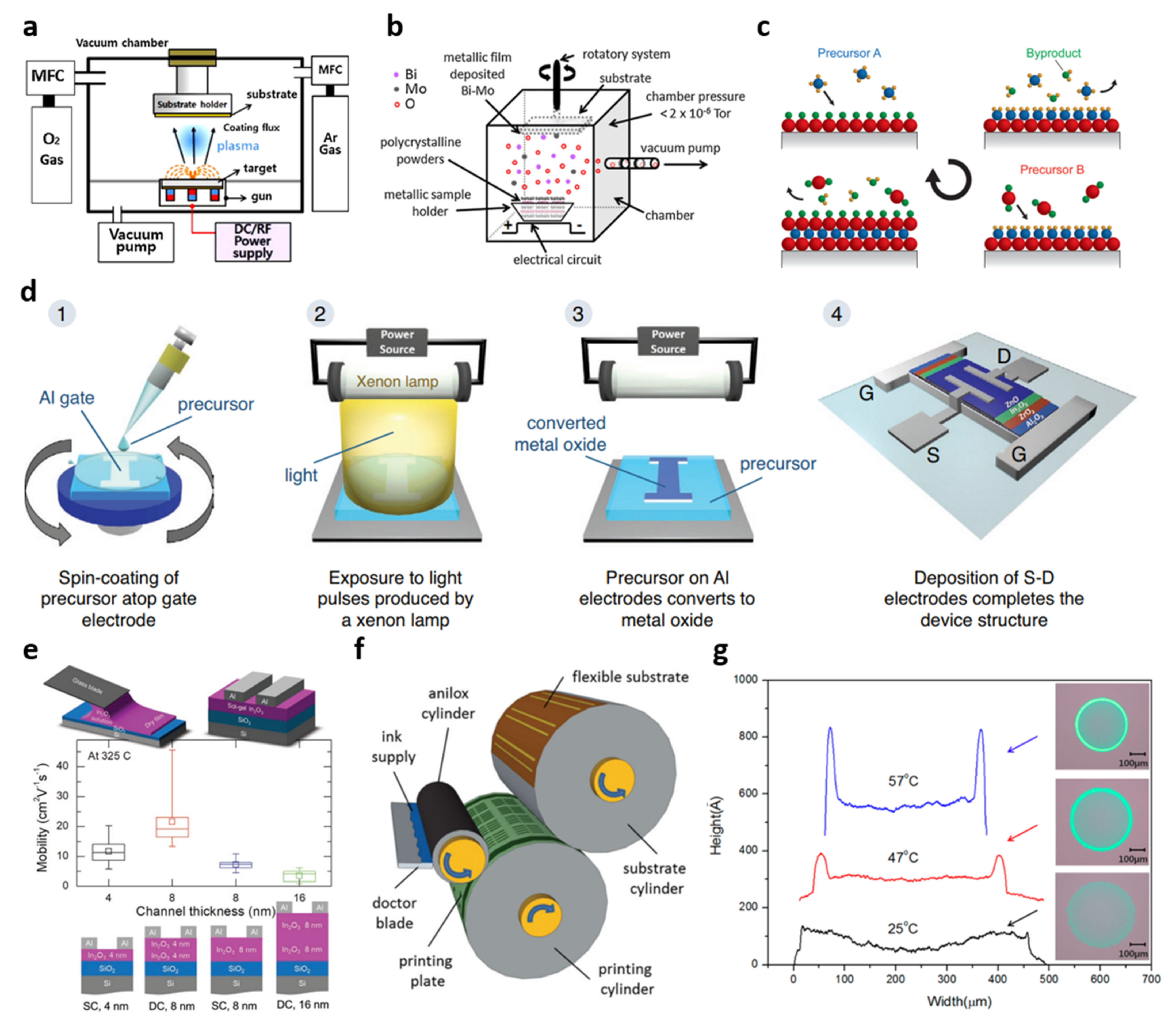
Synthesis methods of metal-oxide semiconductors are divided into a vacuum-based process including sputtering method, thermal evaporation method, and atomic layer deposition (ALD) method (Figure 1a–c) [22,23,24] and solution-based process (Figure 1d–g) [25,26,27,28]. The sputtering method uses plasma to separate material from a target surface and the material particles are deposited on a substrate [29]. The film fabricated by sputtering has the advantages of excellent adhesion to the substrate and uniformity of the deposited film. Thermal evaporation and electron beam evaporation are methods enabled by evaporated materials using a resistive heater and electron beam [30]. The evaporation method has the advantage of low consumption and could apply to most of materials. The ALD method produces an atomic layer unit thin film by repeating precursor and reactant supply and purge cycles [31]. The thin films fabricated with ALD method rarely occur step coverage issues and pinholes. As a result, vacuum-based process methods enable to secure highly uniform film quality.
Recently, a solution-based process for metal-oxide semiconductor thin film has been actively studied. Additionally, the solution process has various methods for fabricating metal-oxide semiconductors such as spin coating [25,32,33,34,35], spray coating [26,36], blade coating [37,38], flexographic printing [27], and inkjet printing [28,39]. Most solution-based processes have advantages for manufacturing flexible and printable devices because of the low annealing temperature. Moreira et al. fabricated solution-based IGZO films with a 300 °C annealing process [40]. Song et al. demonstrated a flexible transistor by annealing ZnO at 200 °C [41]. Yarali et al. demonstrated high-k dielectrics Al2O3/ZrO2 bilayer and In2O3/ZnO heterojunction channel layers-based transistor using spin coating and photonic process (Figure 1d) [37]. Wang et al. presented transistors based on IZO and IGZO using spray-combustion synthesis (SCS) [26]. Kirmani et al. demonstrated an In2O3 semiconductor-based transistor using a blade-coating method. The reported charge mobility of TFT composed of a 4 nm-thickness double-stacked In2O3 was 45.5 cm2 V−1 s−1 (Figure 1e) [38]. Leppäniemi et al. used a flexographic printing process and in-nitrate precursor solution to form a nanocrystalline In2O3 semiconductor layer (Figure 1f) [27]. Twyman et al. deposited In2O3 on glass, PI, and PEN substrates using In(NO3)3 precursors, and replaced the annealing method with a xenon flash lamp photonic sintering method [42]. Lee et al. demonstrated an In2O3 semiconductor-based transistor by inkjet printing [28]. Figure 1g shows surface profiles of single droplets according to various substrate temperatures. The droplets have different morphological characteristics depending on the temperature of the substrate. Table 1 summarizes the electrical characteristics of metal-oxide semiconductor by the fabrication process method.
2.2. Flexible Device
The interest in flexible electronic transistors is increasing due to the demands of individual consumers. Flexible substrates, such as polyimide (PI), polyethylene terephthalate (PET), polyethylene naphthalate (PEN), polytetrafluoroethylene (PTFE), and polydimethylsiloxane (PDMS) are used instead of the conventional rigid substrates to realize flexible electronics. However, since flexible substrates generally have lower thermal resistance than that of rigid substrates (i.e., silicon and glass), it is relatively difficult to implement stable transistor operation [46,47,48,49]. Metal-oxide semiconductors that can be processed at low temperatures (<350 °C) and offer stable electrical performance are promising active materials for flexible transistors. Therefore, an amorphous metal-oxide semiconductor-based transistor is capable of large-area and low-temperature processing, making it possible to fabricate a device on a plastic-based substrate [50,51,52]. This section introduces an oxide semiconductor-based flexible electronic device.
Hwang et al. fabricated an In2O3-based flexible transistor on a PEN substrate (Figure 2a) [53]. The device showed a charge mobility of 3.14 cm2/Vs and a subthreshold voltage of 158 mV/decade despite the bending test. In addition, the device had a stable Ion/off ratio of 109 or higher under bias stress. Recently, inkjet printing technology has been used to manufacture transistor arrays and integrated circuits with high electrical performance and high resolution with a low-cost process [54]. Kim et al. produced flexible semiconductors by depositing an In2O3 semiconductor on PI substrates using inkjet printing technology [55]. Under the condition of a bending radius of 3.5 mm (tensile strain 0.03%), the mobility (5 cm2/Vs) and Ion/off ratio (105) were measured using a bending test. The electrical properties of the device were retained despite the repeated bending tests.
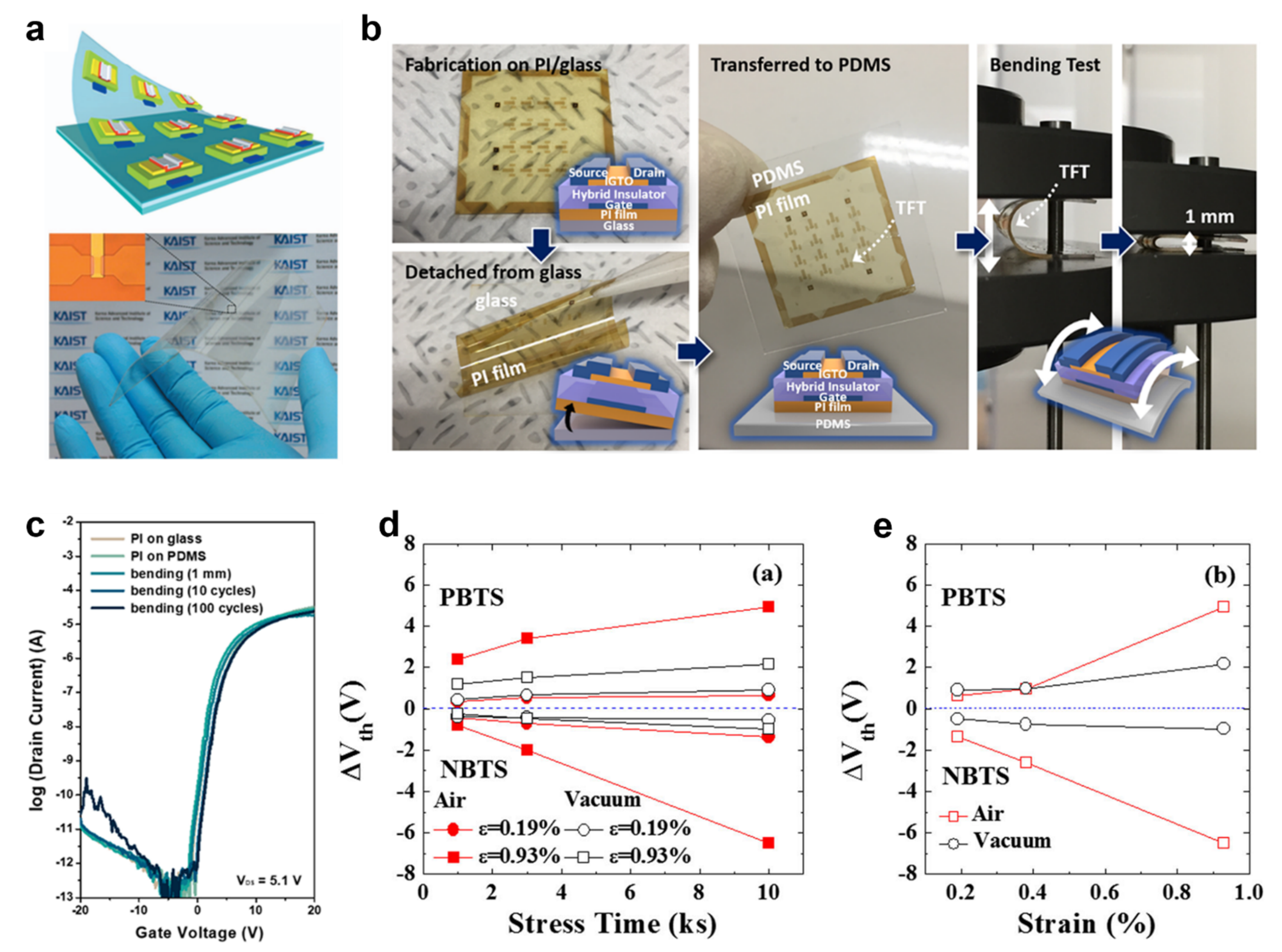
Hur et al. fabricated an indium gallium tin oxide (IGTO) transistor using a H50UV hybrid dielectric film on a PI/Polydimethylsiloxane (PDMS) substrate (Figure 2b,c) [56]. High insulating characteristics of the hybrid gate dielectric films were improved significantly with the reduction of residual hydroxyl groups due to the combination of highly ionic hafnium oxide by a UV treatment. Accordingly, a film having excellent interfacial matching with the IGTO channel layer and a high density was produced. As a result, the device using the hybrid dielectric film had a high mobility up to 25.9 cm2/Vs and an Ion/off ratio of more than 107. Furthermore, the device showed stable transistor operation even in the bending test repeated 100 times under a radius of curvature of 1 mm. Jung et al. reported a flexible indium gallium zinc oxide (IGZO) thin-film transistor on a PI substrate (Figure 2d,e) [57]. Compared to conventional amorphous silicon, the device had a mechanically flexible property as well as a high mobility up to 12.5 cm2/Vs with ε = 0.19%, and low process temperature and uniformity. In the bias temperature stress (BTS) condition, the device was subjected to tensile strain while applying a gate voltage of ± 20 V at 60 °C for 10,000 s in the same negative and positive conditions. In addition, comparison measurements were taken in a 100 mTorr vacuum and an air environment (relative humidity: 30%) to analyze the influence of the air exposure. The Vth increased from −0.5 to −0.97 V as the strain changed from 0.19% to 0.93% in a vacuum ambient. When measured in air, after positive bias temperature stress (PBTS) the device with ε = 0.19% and ε = 0.93% showed a Vth shift of 0.65 V and 4.96 V, respectively.
2.3. Stretchable Device
A stretchable device is considered as a next-generation electronic device in which the electrical characteristics of the device are maintained despite being stretched or bent [58]. The stretchable technology easily reduces the lifespan and destroys the device structure as the physical stress applied to the device is considerably larger than the conventional flexible technology that bends or rolls. Most of previous studies have focused on developing mechanically stable devices when physical deformation, such as using flexible substrates, modifications in the device structure, and tuning in materials, to realize highly robust devices with stretchability [59]. In this context, this chapter introduces metal-oxide semiconductor-based stretchable electronic devices.
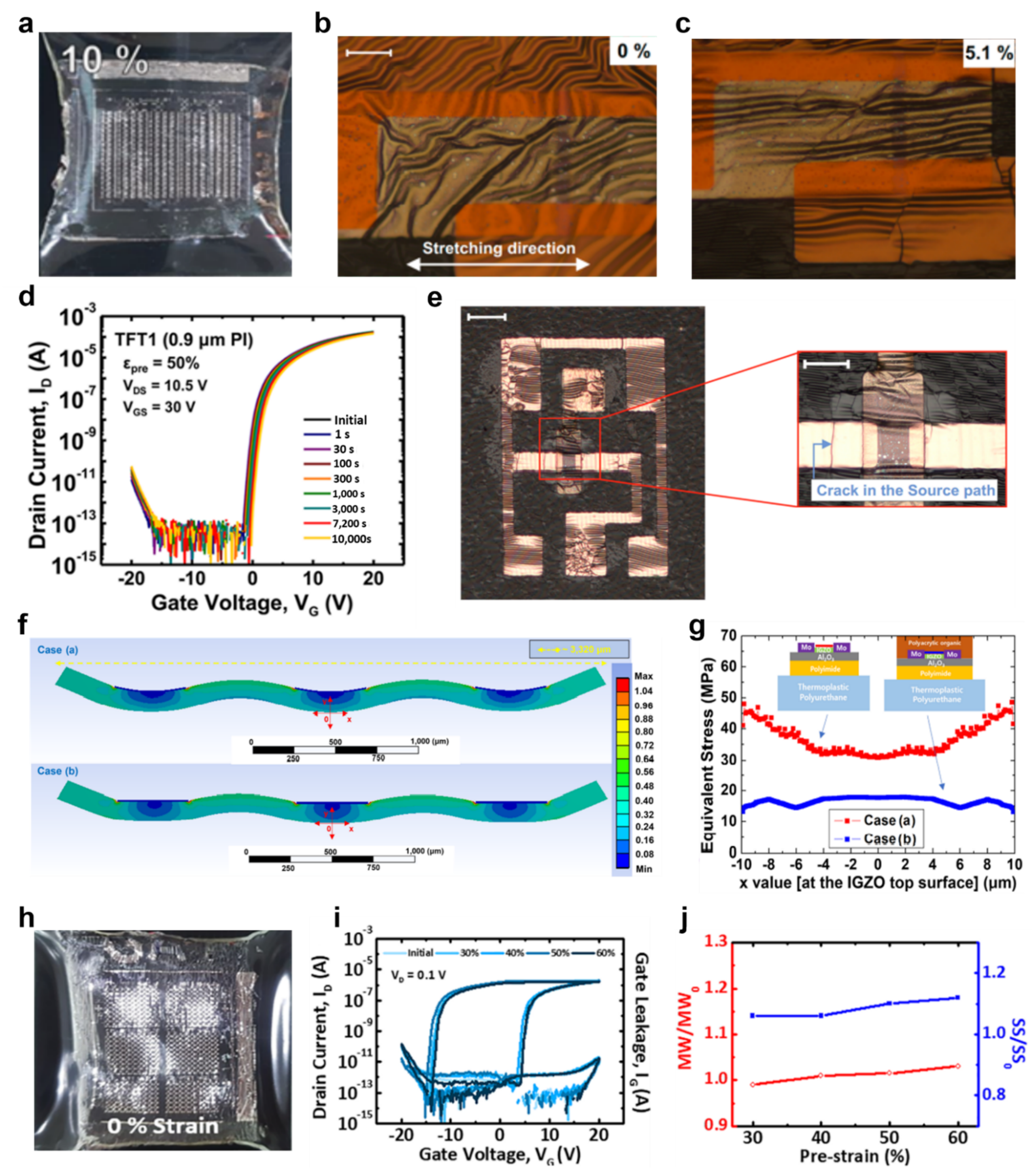
Jang et al. reported an IGZO-based TFT with a wavy-dimensional structure using a PI film (Figure 3a,d) [60]. The IGZO-based TFT showed excellent device operation robustness under compression/stretch conditions with a strain of 40%. In addition, as a result of comparison according to the thickness of the PI film (2 and 0.9 μm), the thinner the film, the more stable the operation when stretching. Park et al. implemented a stretchable active matrix with a novel fabrication technique [61]. After producing all the other components on a rigid substrate, they used a photolithography-based technique to form liquid metal wiring interconnects. Highly conductive and intrinsically flexible liquid metal interconnects can be integrated monolithically with TFT arrays. The fabricated stretchable TFTs had no deformation during elongation up to 40% in the semiconductor region and no deformation after elongation of 20% in the electrode region. At higher tensile strains, some cracks began to appear. The device was manufactured in a 4 × 4 matrix, and it operates stably, even at a maximum strain of 40%, and the threshold voltage and mobility were maintained unchanged. Cantarella et al. fabricated a wrinkled surface on PDMS, implementing a TFT and circuit based on IGZO, and induced stretching in random directions (Figure 3b,c,e) [62]. To fabricate a corrugated surface, the elastomeric surface showed a similar thickness to that of the silica layer in proportion to the oxidation time. This process resulted in surface wrinkling. As a result, it was possible to bend up to 13 μm and maintain its electrical properties while stretching up to 5%, as shown in the Figure 2c. Cracks formed when bent more than 5%, as shown in Figure 2e. No degradation in performance was observed, even when attached to an artificial wrist.
Han et al. reported the electrical characteristics of flexible transistors by stacking IGZO on a PI substrate and implemented stretching simulations for two cases (with or without organic passivation layer) (Figure 3f,g) [63]. In this simulation, even after 10,000 cycles repeated stretching tests at 30% extension, there was no change in the electrical properties in either case. Furthermore, the organic passivation layer reduced the mechanical stress applied to the IGZO. An examination of the change in stress applied to the upper surface of IGZO revealed a decrease in stress at the center from 30.7 to 17.4 MPa. Based on the observed result, it is indicated that the organic passivation film enables the reduction of the mechanical stress applied to the inorganic material layer under both bending and stretching conditions.
Kim et al. fabricated a charge trapping memory thin-film transistor (CTM TFT) with a wavy-dimensional structure using IGZO and zinc oxide (ZnO) (Figure 3h-j) [64]. IGZO was used as the channel layer, and ZnO was used as the channel trap layer. The wavy-dimensional structure allows the device to withstand significant mechanical strain by reducing the applied strain force. As a result, the CTM TFT had a wide memory window of 23.8 V and obtained a large switching current ratio of 106 with a short program pulse of 1 μs. In addition, the transistor showed excellent stretching durability over 150,000 times through optimization of process conditions even at an elongation of 50%. Sim et al. attempted to improve the flexibility by fabricating indium zinc oxide (IZO) TFTs with an open mesh configuration, similar to a kirigami structure [65]. The manufactured IZO TFT had a mobility and threshold voltage of 2.24 cm2/Vs and 4.4 V, respectively. When IZO TFT was stretched, the mechanical elasticity was obtained up to 30%, and stable device operation was achieved. In addition, the ultra-thin thickness and open mesh geometry allowed firm adhesion to human skin without the need for additional adhesives. They could withstand rinsing in water and washing with soap.
2.4. Transparent Device
Metal-oxide semiconductors, such as IGZO, ZnO, zinc tin oxide (ZTO), and tin monoxide (SnO), offer attractive and potential possibilities for transparent electronic devices. Most metal-oxide semiconductors have high optical transmittance in the visible region because of the wide bandgap at more than 3 eV [66,67]. This optically superior metal-oxide semiconductor material can be applied to various industrial technologies, such as smart windows, wearables, transparent displays, and has been actively studied. The analysis of the transmittance of metal-oxide semiconductor TFT is summarized in Table 2. This chapter introduces a transparent transistor with metal-oxide semiconductors.
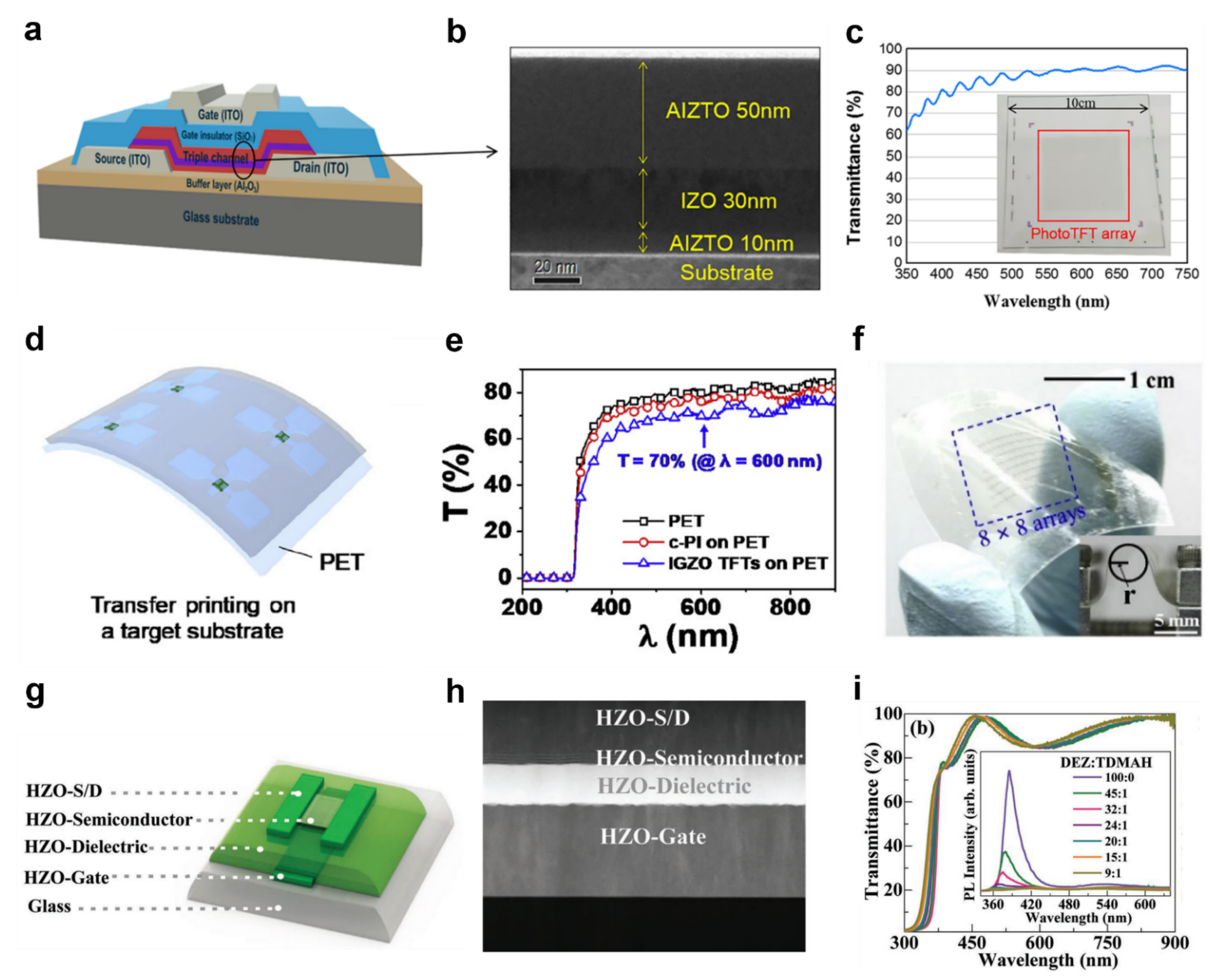
To utilize metal-oxide -semiconductor transistors as transparent display backplane devices, it is necessary to use a metal-oxide-semiconductor material and a material with high optical transmittance for the electrode and insulating film layer, respectively [68]. Lee et al. reported a transparent phototransistor using a three-layer heterojunction metal-oxide semiconductor based on Al: InZnSnO/InZnO/Al: InZnSnO. Figure 4a shows a schematic diagram of an AlZTO/IZO/ALZTO TFT. ITO was used as the source, drain, and gate electrodes, and SiO2 was used as the insulating layer. Figure 4b shows a transmission electron microscopy (TEM) image of all the layers used for the three-layer heterojunction metal-oxide semiconductor TFT. Figure 4c presents a phototransistor array with a 300 pixels per inch (PPI) resolution and 80% optical transmittance [69].
In addition, a metal-oxide semiconductor transistor was applied to transparent flexible substrates, such as PDMS, PI, and PET [70,71,72]. Transparent and flexible transistors bring freedom from morphological limitations caused by conventional rigid substrates and are applied to foldable, flexible, and portable electronic devices. Yoon et al. reported an IGZO-based deep ultraviolet (DUV) photodetector using a CPI and PET substrate. Figure 4d presents a schematic diagram of a transparent and flexible device that uses an ITO electrode. The DUV photodetector fabricated on the PET and CPI substrates showed superior optical transmittance of approximately 70% when the wavelength of light was 600 nm (Figure 4e). As shown in Figure 4f, an 8 × 8 IGZO TFT array fabricated on a PET substrate performed a mechanical bending test and exhibited stable electrical operation at a bending radius of r = 1.4 mm [73].
Figure 4.
(a) Schematic diagram of an AlZTO/IZO/ALZTO TFT; (b) Cross-section TEM image of the channel layer; (c) Transmittance of a phototransistor array with 300 pixels per inch (adapted from [69] with permission from the American Institute of Physics); (d) Schematic diagram of a transparent and flexible device; (e) Transmittance of DUV photodetector fabricated on the PET and CPI substrate; (f) 8 × 8 IGZO TFT array fabricated on a PET substrate. The inset shows bending the device in tensile mode, where r is a bending radius (adapted from [73] with permission from the Elsevier B.V.); (g) Schematic diagram of an HZO-based TFT; (h) Cross-section TEM image of HZO-based TFT; (i) Transmittance of the conducting HZO film (adapted from [74] with permission from the John Wiley and Sons).

The use of representative metal-oxide semiconductors containing indium, such as IGZO, ITO, and IZO, are limited due to their environmental issues (i.e., toxicity), scarcity of indium, and high cost of indium. Therefore, there has been considerable research on transparent metal-oxide semiconductor electronic devices using low toxicity and abundant materials. Alshammari et al. reported a process system in which the gate, source, drain, semiconductor, and insulating film layer constituting the transistor were all made of a hafnium zinc oxide (HZO) (Figure 4g) [74]. This study used HZO, which consists of zinc and hafnium with relatively low toxicity. The conductivity of HZO was controlled by the composition ratio of the two chemical precursors (DEZ) (C2H5)2 Zn and (TDMAH) C8H24HfN4. All layers of the HZO-based TFTs were confirmed by high-resolution electron microscopy (Figure 4h). Figure 4i shows the transmittance of the conducting HZO film in the visible region and has high optical transmittance of approximately 90%.

Table 2.
Transmittance of metal-oxide semiconductor-based transistors.
| Materials | Gate Electrodes |
Source/Drain Electrodes |
Dielectric Layer | Substrate | Semiconductors Transmittances (Visible Region) | Ref |
|---|---|---|---|---|---|---|
| IGZO | ITO | IGZO | Al2O3, PMMA | Glass | Over 80% | [75] |
| IGZO | Al | Al | Al2O3 | Quartz-coated glass | Over 98% | [76] |
| IGZO | ITO | Al | Ta2O5, Si3N4, SiO2 | ITO coated glass? | Over 80% | [77] |
| IZO | Si | Al | HfO2 | Si wafer | Over 90% | [78] |
| GZO | P+-Si | Au/Cr | Al2O3 | Si wafer | Over 80% | [79] |
| NiOX | P+-Si | Ni | Al2O3 | SiO2 wafer | Over 90% | [80] |
| SnO2 | P+-Si | Au | SiO2 | SiO2 wafer | Over 97% | [81] |
| ZTO | P+-Si | Al | Al2OX, SiO2 | SiO2 wafer, Si wafer | Over 85% | [82] |
| WZTO | P+-Si | Al | SiO2 | SiO2 wafer | Over 85% | [83] |
3. Integrated Circuits
3.1. Inverter
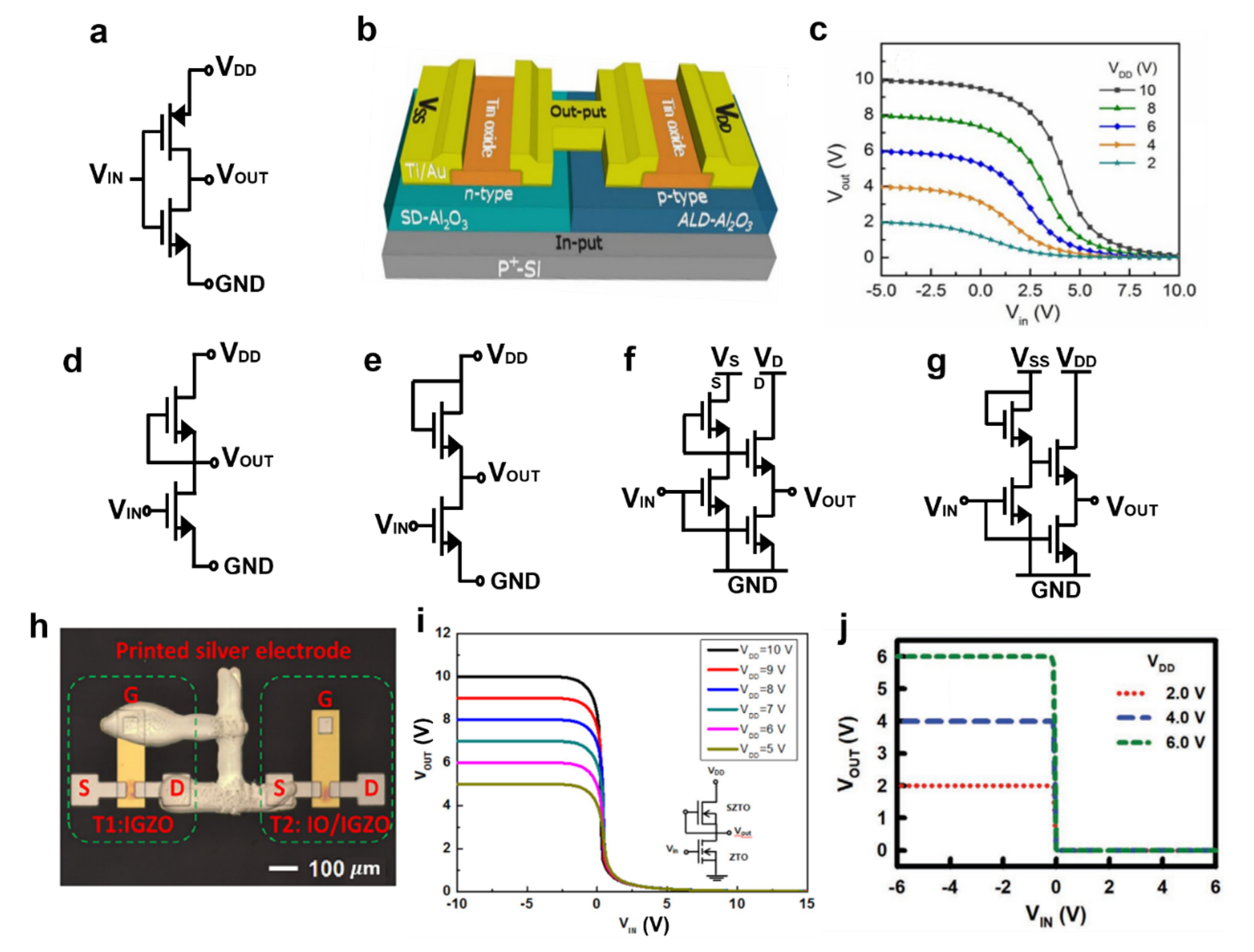
An inverter is a logic element in which output voltage has a value opposite to the input voltage and is the most basic circuit for designing a logic circuit [84,85,86]. A complementary metal-oxide-semiconductor (CMOS) inverter logic device consists of one n-type metal-oxide semiconductor (NMOS) as a pull-down operation and one p-type metal-oxide semiconductor (PMOS) as pull-up operation (Figure 5a). Most metal-oxide semiconductors, such as IGZO, ZTO, and ZnO, exhibit typical n-type characteristics. On the other hand, there are fewer p-type oxide semiconductor materials for implementing the PMOS [87]. Owing to the limitations of these semiconductor materials, research to implement inverters with only n-type oxide semiconductors is being actively conducted [88]. The four circuit schemes were reported: (1) zero-VGS, (2) diode-load, (3) Pseudo-D, and (4) Pseudo-E (Figure 5d–g). This chapter introduces an inverter based on a metal-oxide semiconductor.
Nayak et al. controlled the concentration of OH groups in the gate dielectric to control the carrier polarity and accordingly implement controllable n-type and p-type TFTs with the CMOS inverter circuit (Figure 5b) [89]. Tin oxide was used for both the n-type and p-type TFTs; the semiconductor properties were controlled by modulating the concentration of OH groups in the gate dielectric. ALD-Al2O3 operating in depletion mode exhibited p-type transistor characteristics, and SD-Al2O3 operating in enhancement mode exhibited n-type characteristics. The resulting CMOS inverter showed a typical inverter response and a gain of ~3 v/v. Although the gain was low, it illustrates the novel approach of the co-formation of n-type and p-type channel layers.
Shao et al. presented a large-scale, high-performance IGZO dot TFT using inkjet printing technology and implemented an NMOS inverter (Figure 5h) [90]. The mobility of the IGZO TFT was reported to 28.44 cm2/Vs. The TFT showed an excellent Ion/off ratio (>108) and no hysteresis. The inverter showed performance at a maximum voltage gain of 112 V/V. Han et al. implemented a high-performance inverter composed of ZTO TFTs and SZTO TFTs (Figure 5i) [91]. The ZTO TFT was operated as a driver transistor in enhancement mode, and the mobility was obtained to 23.6 cm2/Vs. The SZTO TFT operated as a load transistor in the depletion mode, and the mobility was 18.4 cm2/Vs. The inverter showed a high voltage gain of 25.22 v/v and a narrow transition width at an operating voltage of 10 V. Islam et al. fabricated a-IGZO TFT from high dielectric constant zinc aluminum oxide (ZAO) using low-cost spray pyrolysis technology for large area and low power (Figure 5j) [92]. The fabricated TFT had a mobility of 15.04 cm2/Vs and a high Ion/off ratio (>108). The voltage gain of the inverter was 58 v/v at an operating voltage of 6 V. This high voltage gain was similar to other inverters based on a SiO2 gate dielectric but had a significantly lower operating voltage. This material has significant potential for display applications in low power consumption electronics [93].
A pseudo inverter is more complicated than a zero-VGS inverter but has higher noise immunity and a larger output swing. Hu et al. fabricated a TFT based on ITO stabilized ZnO and implemented a pseudo-NMOS inverter [94]. ITO-stabilized ZnO exhibited excellent spatial uniformity, air stability, repetitive switching characteristics, and consistent electrical performance. The pseudo-NMOS inverter had a delay time of 1.6 μs when the operating voltage was 5 V and a delay time of 0.8 μs when the operating voltage was 10 V. Two-input and three-input XOR gates were also implemented. When the operating voltage was 10 V, the two-input XOR gate had a delay time of 2.25 μs, and the three-input XOR gate had a delay time of 3.47 μs. This inverter will be used with other logic circuits to perform more complex functions.
3.2. Ring Oscillator
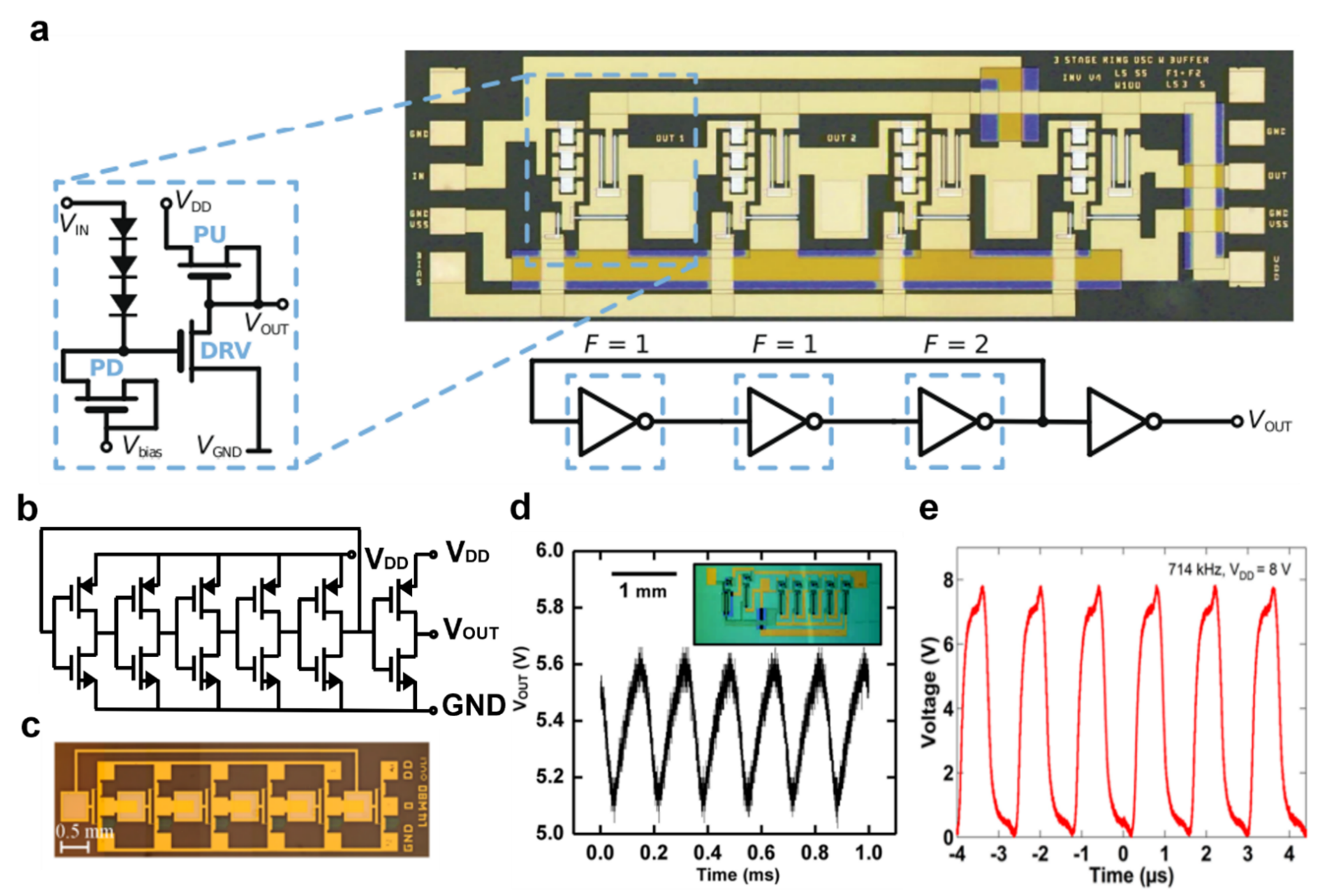
A ring oscillator is a circuit component in which an odd number of inverters are configured in a ring structure, and the output of the last inverter is feedback to the first inverter. When ‘HIGH’ is input, ‘LOW’ is output, and vice versa. As this operation is repeated through feedback, it oscillates between the two voltage levels representing ‘HIGH’ and ‘LOW’ [95]. The main purpose of the ring oscillator is to measure the effects of voltage and temperature on a chip and is used mainly to generate a clock signal [96]. Table 3 summarizes the analysis of the ring oscillator made of a metal-oxide semiconductor.
Lahr et al. fabricated a three-stage ring oscillator composed of a ZTO-based metal-semiconductor field-effect transistor (MESFET) (Figure 6a) [97]. Using the Schottky diode FET logic (SDFL) method, the level shift of the output signal was promoted so that the series connection of the inverters could be cascaded successfully. The mobility of the fabricated ZTO MESFET was reported to 1.8 cm2/Vs, and the threshold voltage was −0.6 to −0.3 V. In the ring oscillator VDD = 3 V, the maximum oscillation frequency was 451 kHz, and the delay time was 277 ns.
Kim et al. fabricated an inverter and a five-stage ring oscillator by combining n-type ZTO and p-type single-wall carbon nanotubes (SWCNTs) (Figure 6c,e) [99]. Both n-type and p-type are solution processable and were deposited by inkjet printing. Among them, the mobility of ZTO TFT was 4.4 cm2/Vs, and the Ion/off ratio was 2.6 × 10⁶. The output signal showed a relatively high oscillation frequency, reaching 714 kHz at VDD = 8 V. Hence, the complementary circuit technology could operate in air. With a delay time of 140 ns, this is the fast-ring oscillator circuit.
Jin et al. implemented a water-soluble TFT using IGZO and a five-stage ring oscillator (Figure 6d) [98]. The mobility of the transistor was 10 cm2/Vs, the Ion/off ratio was 2 × 10⁶, and the manufactured ring oscillator was measured to 5.67 kHz at VDD of 19 V based on water-soluble thin-film transistors. The fabricated transistor showed complete circuit dissolution, starting with the disassembly of the polyvinyl alcohol (PVA) substrate within 30 min in di water. This suggests the possibility of environmentally absorbable technology.
Table 3.
Ring oscillator characteristics.
| Materials | # of Inverter | VDD (V) | Frequency (MHz) | Delay Time (ns) | W/L (μm) | Ref |
|---|---|---|---|---|---|---|
| ZTO | 3 | 3 | 0.451 | 277 | 100/5 | [97] |
| a-IGZO | 5 | 19 | 0.00567 | - | 270/10 30/10 | [98] |
| ZTO, SWCNTs | 5 | 8 | 0.714 | 140 | 80/4 | [99] |
| IZO | 11 | 5 | 0.132 | - | 40/10 20/10 200/10 | [100] |
| IZO | 7 | 20 | 2.66 | 27 | 35/7 70/7 153/7 | [101] |
| ITO-stabilized ZnO | 13 | 10 | 0.042 | 920 | 20/10 160/10 | [102] |
| a-IGZO | 23 | 18 | 2.4–3 | - | 20/6 | [103] |
3.3. NAND, NOR Gate
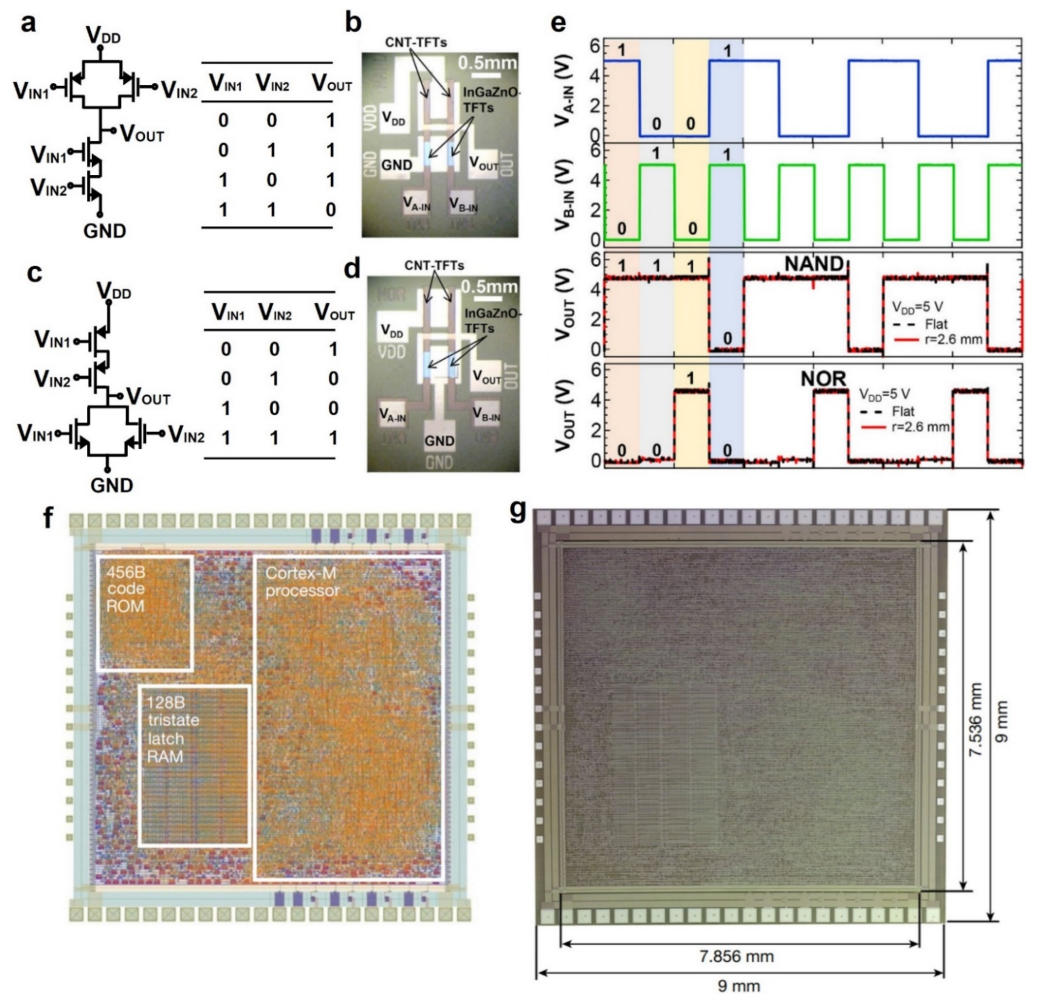
Computing devices, such as smartphones and tablet computers, can be realized by the miniaturization of transistors and the implementation of integrated circuits. Logic gates are essential elements for enabling these computing devices, with the NAND gate and NOR gate being the most basic [104]. The NAND gate is a circuit in which ‘0’ is the output only when both input values are ‘1’, and ‘1’ in all other cases (Figure 7a). The NOR gate is a circuit that outputs ‘0’ only when both input values are ‘1’, and ‘1’ in all other cases (Figure 7c) [105].
Honda et al. fabricated flexible CMOS using the n-type IGZO and p-type CNTs. They confirmed the operation of the NAND and NOR gates (Figure 7b,d) [106]. The Ion/off ratio of the IGZO TFT was ≥105, and the mobility was 5.5 cm2/Vs. The CNTs TFT had an Ion/off ratio of more than 104 and a mobility of 2.2 cm2/Vs. In the NAND and NOR gates, the input voltages were 0 V and 5 V, and are indicated as ‘0’ and ‘1’, respectively. (Figure 7e). The same logical value was obtained even under the bending condition of r = 2.6 mm compared to the flat case. Few flexible CMOS NAND and NOR operations have been reported, but this study has demonstrated the flexible CMOS NAND and NOR operations.
Liu et al. reported NAND and NOR circuits using only ZnO nanorod materials [108]. Unlike the basic CMOS mechanism, the piezoelectric field-effect transistor (PFET) controls on/off with the strain of the substrate. It is indicated as a logic ‘0’ in the compressed state, and a logical ‘1’ in the stretch state. An inverter can be implemented by stacking ZnO and electrode equally above and below the Kapton substrate. In addition, NAND and NOR circuits were fabricated using the two fabricated devices. As a result, the output was ‘0’ when the strain was less than 0.8%, and close to ‘1’ when it was not. Accurate circuit operation was realized. A characteristic is that the response time was determined by the ratio of the mechanical signals rather than electrical signals. Finally, XOR, multiplexer (MUX), and demultiplexer (DEMUX) were all realized. This increases the possibility of future applications of micro-electro-mechanical system (MEMS) devices by constructing circuits using only a single material.
Microprocessors are at the cire of all electronic devices, including smartphones, cars, routers, and smart objects. Biggs et al. recently fabricated a flexible core (PlasticARM) with a 32-bit central processing unit (CPU), system-on-chip (SoC), and CPU peripherals using IGZO TFTs (Figure 7f,g) [107]. The plasticARM contained 18,334 NAND gates, making it a complex FlexIC built with metal-oxide TFTs on a flexible substrate. The output was 12 times higher than previously reported integrated circuits [15,109]. In addition, compatibility allowed piggybacking of conventional software/tool support, such as compilers. This will pave the way for developing flexible, low-cost, smart integrated systems that will enable the ‘Internet of Everything’ over the next decade.
4. Biosensors Applications
Recently, the development of intelligent biosensors that effectively monitor human biological conditions, such as viruses, diabetes, and cancer is important [110,111,112]. The biosensor is a system that transduces a response between the target material and selective receptor into the signal to confirm the presence of the target material. Parameters, such as real-time monitoring, sensitivity, and reproducibility, are important indicators determining the performance of a biosensor. The transistor-type biosensor effectively detects the presence or absence of the target material by changing the conductivity with the presence of functional groups or receptors in the semiconductor channel [113]. This chapter presents diverse biosensors that applied metal-oxide semiconductors with excellent electrical properties, high electron mobility, and strong chemical resistance.
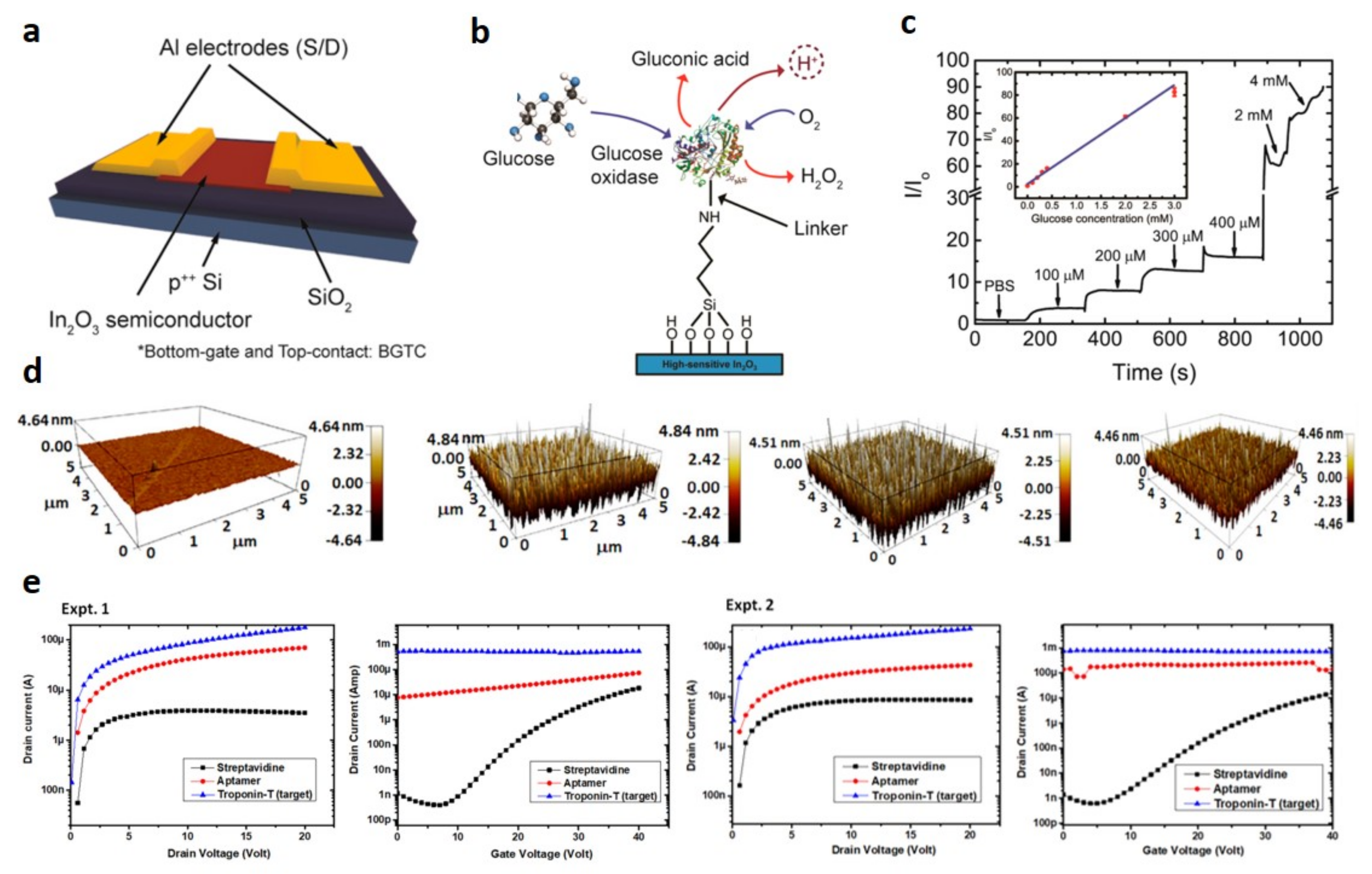
Rim et al. fabricated an In2O3-based ultra-thin conformal biosensor using simple solution processing (Figure 8a–c) [114]. The In2O3-based field-effect transistor (FET) showed a mobility of 20 cm2/Vs and a high Ion/off ratio (>107). The biosensor measured the concentrations of Ph and D-glucose, while the self-assembled monolayer of NH2-terminated silane acted as a pH sensor. When the pH was measured from 9.0 to 5.5 at 0.5 intervals, the drain current response increased with decreasing pH. In addition, a change was observed when the concentration of D-glucose was measured from 100 μM to 4 mM. The proposed device was attached stably to artificial skin and artificial eyes with rough surfaces.
The stability problem of biosensors made from aptamers with high thermal resistance and chemical stability has attracted interest [115,116]. Agarwal et al. reported a ZnO-based transistor that could detect cardiac troponin-T (cTnT) as a biomarker of cardiovascular disease. The channel of the bare ZnO transistor was immobilized in the order of 3-Aminopropyltriethoxysialne (APTES), glutaraldehyde, streptavidin, and biotinylated troponin-T aptamer. Three-dimensional Kelvin probe force microscopy (KPFM) was performed to measure the potential variations of the functionalized device surface (Figure 8d). In addition, the transfer curve and output curve modulated by the biomolecule interactions of the functionalized ZnO transistor were measured (Figure 8e). The variations in electrical characteristics in the two sets of ZnO transistors were measured by drop-casting the analytes. The current level of troponin-T was higher than that with streptavidin and aptamer, highlighting its potential as a sensor for the qualitative detection of cardiovascular disease [117].
Figure 8.
(a) Schematic diagram of the In2O3 FET biosensor; (b) Enzymatic oxidation of D-glucose via glucose oxidase to produce gluconic acid and hydrogen peroxide; (c) Variation of the drain current response with D-glucose concentration (adapted from [114] with permission from the American Chemical Society); (d) The 3D KPFM image of bare ZnO surface, aptamer biofunctionalized surface, aptamer interacting with Troponin-T protein, aptamer biofunctionalized surface interacting with HigG protein; (e) Output and transfer characteristics of a two-set ZnO transistor (adapted from [117] with permission from the Elsevier B.V.).

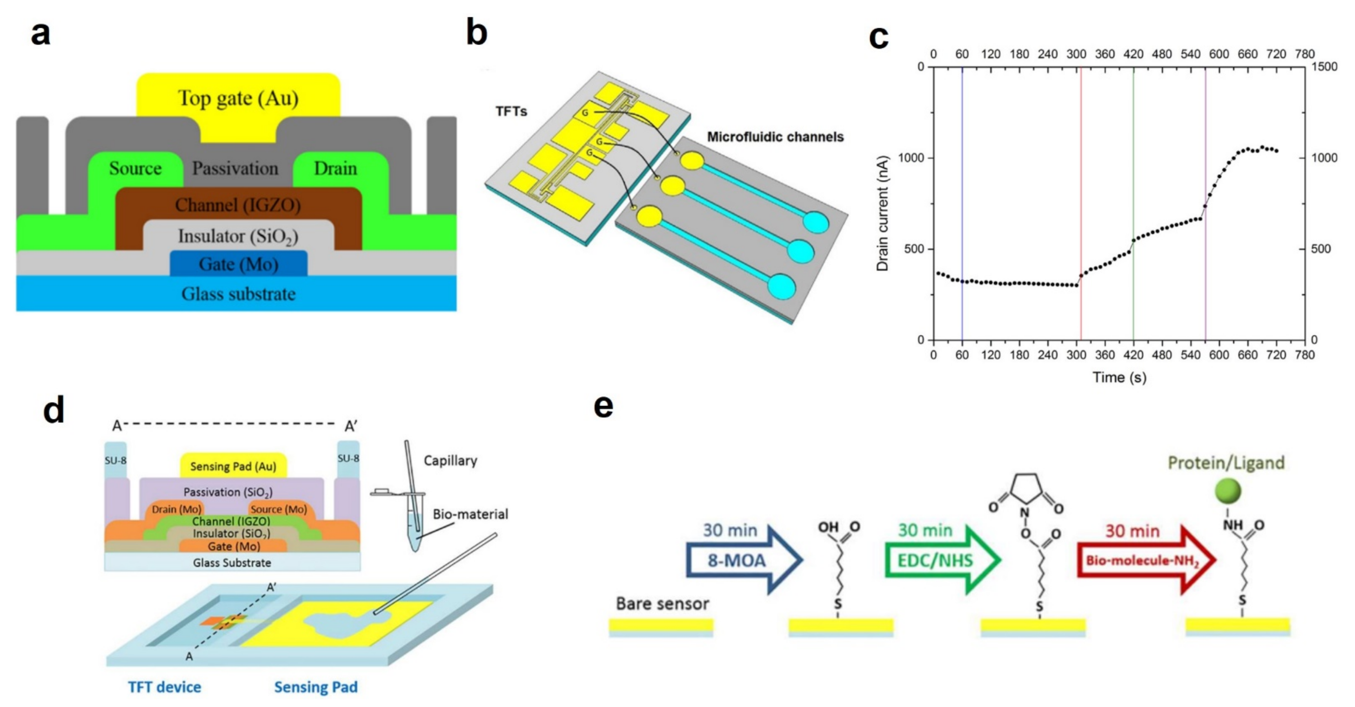
The streptavidin-biotin complex system is useful for purifying or detecting proteins. Chen et al. fabricated an IGZO thin-film transistor-based biosensor with integrated microfluidic channels (Figure 9a,b) [118]. The binding interaction of the streptavidin-biotin complex was analyzed by monitoring the transient response of the transistor current with this biosensor. Figure 9c presents a graph of sampling the drain current every 10 s when a streptavidin-biotin mixed solution was added at VDS = 5 V, VGS = 10 V at 60 s. In the first current increase, the diffusion case of biotin was detected. The diffusion case of streptavidin was detected in the second current increase. The last increase in current was detected in a complex of the two substances.
Wang et al. fabricated an IGZO TFT-based biosensor with gold pads using a malate-aspartate shuttle. The IGZO biosensor detected the biochemical reaction between NADH and NAD+ (Figure 9d,e) [119]. In the proposed device, a gold pad was placed on an IGZO TFT, and 8-mercaptooctanoic acid (8-MOA), ethyl dimethylaminopropyl carbodiimide (EDC)/N-Hydroxysuccinimide (NHS), and NH2 functional groups were added sequentially. Subsequently, the sensor was functionalized when washing unbound molecules to detect the target proteins and ligands. NADH was almost oxidized to NAD+ during the sensing process, and OAA was reduced, causing a change in current. When the linker captured the NAD+ molecule, negative carriers were induced in the IGZO channel, which contributed to the increase in drain current. This led to a better method for identifying the reaction states while providing higher sensitivity than optical spectroscopy.
5. Neuromorphic Application
5.1. Neuromorphic Application by Electrical Operation
The need for an unprecedented transistor system to replace the conventional Von Neumann architecture is emerging because of the limitations of high integration and efficiency of transistors. Among the promising replaced system, the implementation of transistors by a neuromorphic structure that mimics the structure of human neurons and synapses has garnered interest [120]. Although the human brain comprises approximately 100 billion neurons and a trillion synapses, the human brain system shows efficient power consumption compared to the conventional Von Neumann system [121]. In addition, the human brain has superior processing capability in complex cogitation information processing ability than a Von Neumann system. Hence, it is expected that neuromorphic devices can derive similar performance. This chapter describes a metal-oxide semiconductor-based synapse transistor among neuromorphic devices highlighted as a next-generation transistor architecture.
The synaptic transistors require a low current signal for efficient energy consumption. Metal-oxide semiconductors, such as IGZO, have high mobility (>10 cm2 V−1S−1) and low off current (<0.1 nA) characteristics suitable for neuromorphic devices [122,123,124]. Cho et al. reported about 0.269 fJ low energy consumption synaptic transistors applying the IZO/IGZO double-layer structure of an amorphous oxide semiconductor to mimic the plasticity of synapses. The gate electrode is considered a pre-synapse, and the semiconductor layer-source/drain electrode is considered the post-synapse region. In the conductivity of semiconductors considered as the weight of the synapse, the proton act as a medium, inducing a weight change. As a result, the drain current performs the plasticity of the synapse. The synaptic transistor was operated in a similar environment to the human brain (temperature 25 °C, relative humidity 50%). The proposed synaptic transistor had a low energy consumption of 0.269 fJ when performing a spike operation [125].
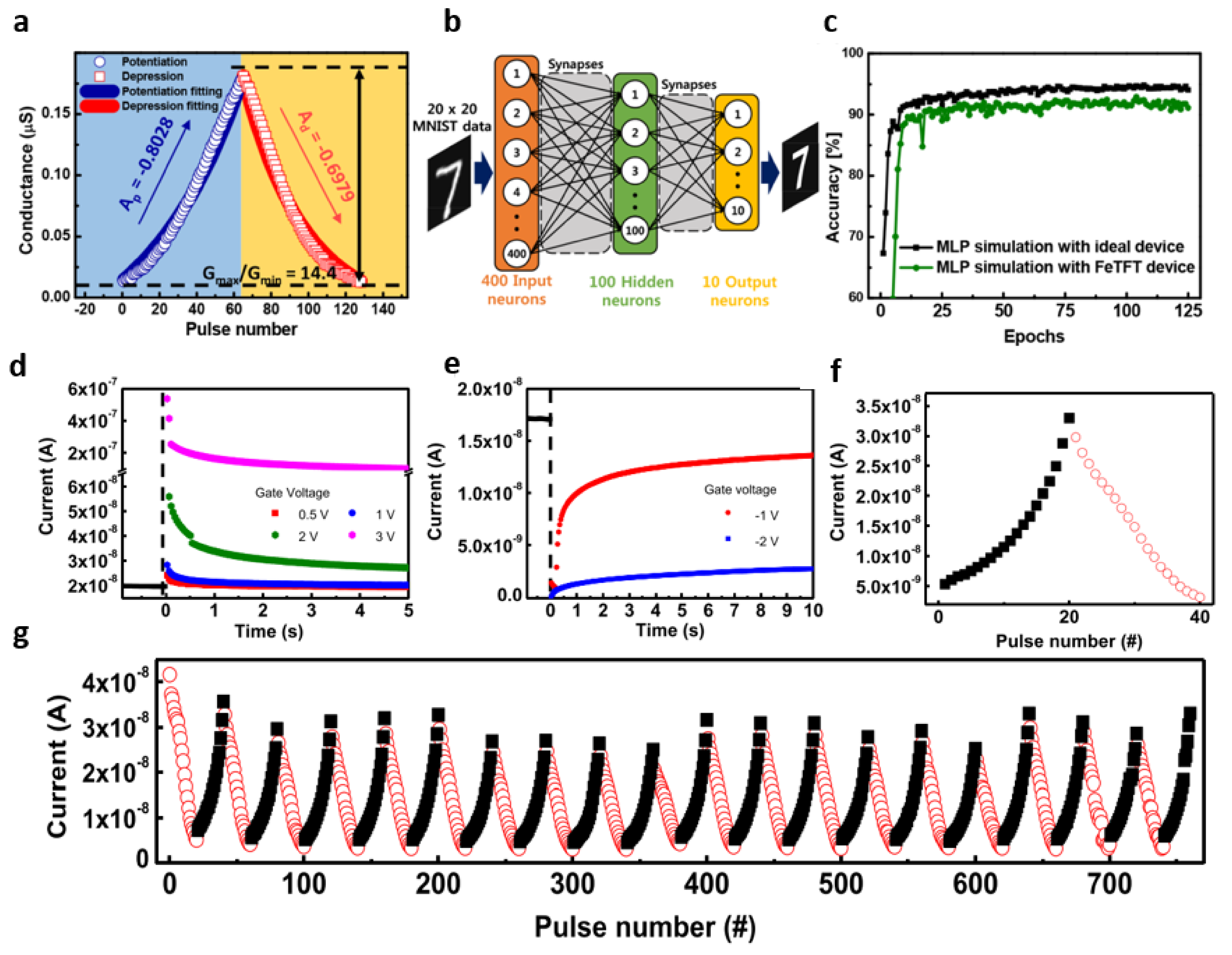
Kim et al. demonstrated ferroelectric thin-film transistor (FeTFT) with metal-ferroelectric-semiconductor (MFS) structure using the hafnium oxide and IGZO. The FeTFT represents the potential of synapse transistors by inducing variation in the channel conductance of IGZO with respect to the polarization state of hafnium oxide. Figure 10a represent the potentiation and depression characteristics through conductance modulation of FeTFT which condition at linearity (Ap, −0.8028; Ad, −0.6979) and Gmax/Gmin ratio > 10. To perform artificial neural network (ANN) simulation, a two-layer multilayer perceptron (MLP) (400 input neurons, 100 hidden neurons), and 10 output neurons were used (Figure 10b). The FeTFT-based synapse transistor has a pattern recognition accuracy of 91.1%, which is similar to ideal neuromorphic device with and accuracy of 91.1% [126].
Several studies have evaluated additional materials for the oxide semiconductor-based devices to enhance the performance of artificial synaptic transistors [127]. Park et al. presented a synaptic transistor with a heterojunction structure made from an oxide semiconductor IGZO and reduced graphene oxide (rGO) with high mobility and stability. The height of the Schottky barrier formed between IGZO and rGO was adjusted to the gate voltage that induced lower power consumption and improved the dynamic range. The long-term potentiation (LTP) transmits repetitive signals between the synapses resulting in efficient signal transduction by strengthening the connection among the synapses. Figure 10d,e show that the spike changed when a positive gate voltage and a negative gate voltage were applied to the synaptic transistor, respectively. Long-term potentiation was observed when a positive gate voltage. On the other hand, long-term depression (LTD) occurred after applying a negative voltage. Figure 10f shows 20 consecutive positive and negative voltage spikes. The gradually changed current levels of the spike were caused by modulating the Schottky barrier height between IGZO and rGO. In addition, Figure 10g shows the 20 consecutive spikes pulses that operate for repetitive 760 cycles without degradation [128].
Figure 10.
(a) Potentiation and depression characteristics of FeTFT with incremental pulse scheme; (b) Schematic illustration of two-layer multilayer perceptron neural network; (c) Simulated pattern recognition accuracy of the two-layer multilayer perceptron neural network based on the ferroelectric FeTFT compared to an ideal neuromorphic device (adapted from [126] with permission from the American Chemical Society); (d) Positive gate voltage spikes (0.5 V, 1 V, 2 V, 3V); (e) Negative gate voltage spikes (−1 V, −2 V); (f) Potentiation and depression characteristics with 20 consecutive positive voltage spikes and negative voltage spikes; (g) Potentiation and depression characteristics under repetitive cycling for 760 pulses (adapted from [128] with permission from the Elsevier B.V.).

5.2. Neuromorphic Application by Photonic Operation
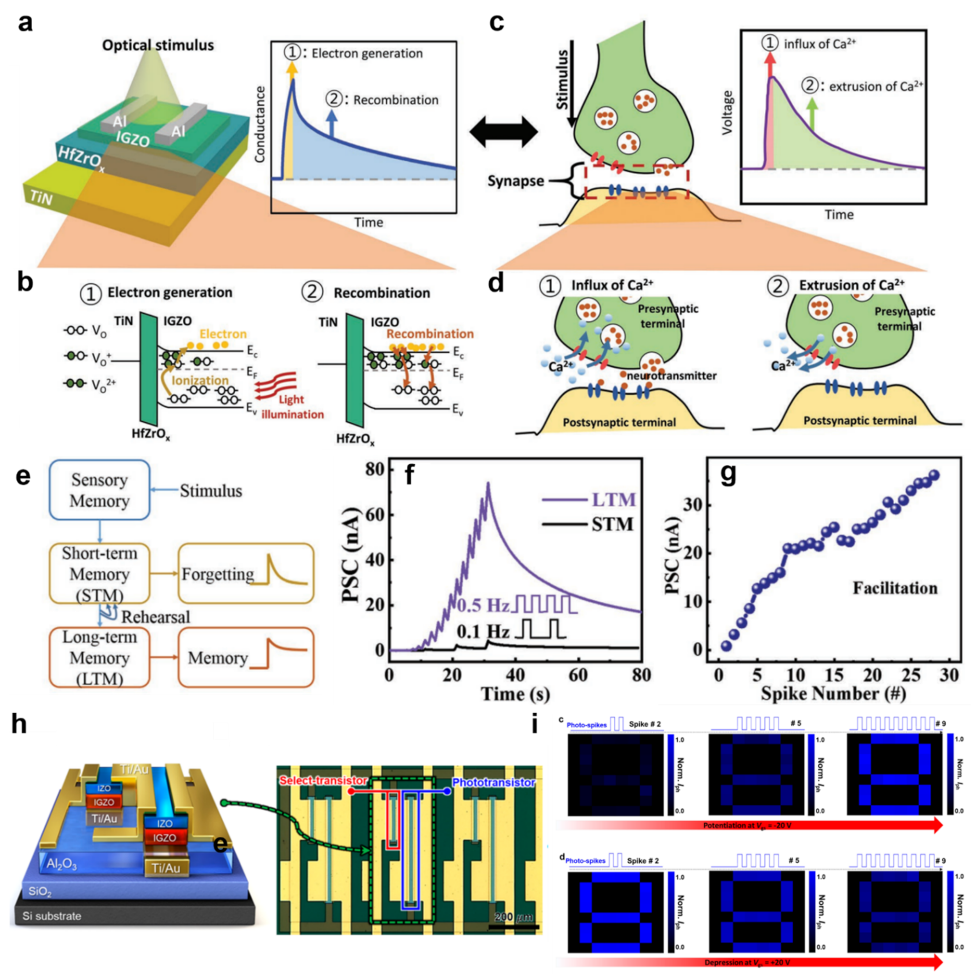
Among the neuromorphic devices that mimic the efficient structure of the human brain, the optical synaptic devices studied have attracted recent interest [19,129,130]. Photo synaptic transistors that are applied with human visual mechanisms have attractive characteristics, such as low power consumption and real-time visual image processing [131]. As a result, photo synapse transistors are the next-generation semiconductor transistors suitable for Internet of Things (IoT) networks and image sensors that generate large amounts of data. Nian et al. reported a photo synapse transistor that mimicked the human visual system. The light that reflects the object passing through the human eye changes the photoreceptors of the visual nervous system. Photosensitive synapses that change the photoreceptors generate and inhibit the short-term post-synaptic currents by taking over-stimulation from the presynaptic neurons. According to this mechanism, the spike generated by the post-synapse current changes the weight of the synapse and causes plasticity of the synapse [132]. This chapter introduces a synaptic transistor based on a metal-oxide semiconductor.
Kim et al. presented a photonic synapse transistor that uses a metal-oxide semiconductor IGZO and ferroelectric HfZrOx layer. The short-term potentiation (STP), LTP, and paired-pulse facilitation (PPF) of the proposed phonic synapse transistor were realized as a response to an applied optical stimulus. The common PPC behavior of IGZO was considered by the ionization of oxygen vacancies. The conductivity of IGZO was increased by optical stimulation, and the increased conductivity decayed with time (Figure 11a). The ionization of oxygen vacancies by optical stimulation generated electrons. The excess generated electrons were released into the bulk IGZO and increased the conductance. In addition, the recombination and neutralization of Vo1+ and Vo2+ occur, resulting in the slow decay of conductance (Figure 11b). The similarity between the photoelectron generation and recombination mechanism and the Ca2+ influx and expulsion mechanism mimics the function of synaptic devices. Figure 11c,d show the biological synaptic structure and the signal transmission mechanism by the synapse. The Ca2+ influx induces an action potential when a certain stimulus reaches the presynaptic membrane. Subsequent release of neurotransmitters can strengthen and weaken the synaptic transitions. On the other hand, changes in the synaptic responsivity persist for a short time because Ca2+ is released to the presynaptic membrane [133].
Wu et al. demonstrated an IGZO-based artificial synaptic TFT which is performing essential behavior of synaptic devices such as PPF, paired-pulse facilitation (PPF), excitatory postsynaptic current (EPSC), short-term memory (STM), and long-term memory (LTM). In addition, the plasticity of synapses was changed by the composition ratio of IGZO film. Figure 11e shows a typical memory model presented by Atkinson-Shiffrin that describes STM and LTM behavior. The changed frequency of UV light pulse stimulation irradiated on IGZO-based synaptic TFT mimics the rehearsal of the human brain to convert STM to LTM. When IGZO-based synaptic TFTs were irradiated with UV light pulses of 0.1 Hz and 0.5 Hz, STM and LTM behaviors were achieved, respectively (Figure 11f). Figure 11g shows the increased synaptic weights with identical photonic simulation [134].
Hong et al. reported a neuromorphic active pixel image sensor array (NAPISA) chip that uses an IGZO/IZO heterojunction-structured metal-oxide semiconductor and ferroelectric layer. The IZO back-channel layer was deposited using a solution process, and the IGZO front-channel layer was deposited by sputtering. Figure 11h presents a schematic diagram of an 8 × 8 NAPISA chip in which each pixel consists of one transistor and a phototransistor, respectively. Figure 11i shows photocurrent mapping images of an 8 × 8 NAPISA chip applied using a pulsed light stencil projection method. In the potentiation mode, the visual information became more apparent as the number of photo spikes increased. By contrast, the depression mode makes visual information indistinct with more photo spikes [135].
6. Conclusions
In summary, this review revisits recent progresses in metal-oxides-based emerging devices. While conventional silicon-based devices suffer from its limited form factor, difficulty in large-area processing, and complicated manufacturing process, the metal oxides are considered to obtain various functionality such as flexibility, transparency, and so on. Based on the merit mentioned above, the metal-oxide semiconductors are achieving various technological developments: (i) flexible and stretchable devices, (ii) integrated circuits, (iii) biosensors, and (iv) neuromorphic devices. Each technology still has challenges. Here are the summarized the pros and cons as follows:
- In recent years, the development of metal-oxide-based TFTs with flexible and stretchable characteristics has been actively studied. However, there are still limitations of insufficient durability of the electronic device due to harsh physical deformation. To be successful in practical applications, it is necessary to develop devices that can withstand further extreme mechanical stress.
- The implementation of integrated circuits based on the metal oxides has been extensively developed. In particular, the recent demonstration of the ARM core is a remarkable achievement. However, a complementary circuit must be developed for reducing a static leakage current and power consumption, and accordingly the development of p-type metal oxides is highly required.
- The interest of biosensor devices using metal-oxide semiconductors is focused. However, the number of selectable materials that capable of binding to target biomaterials are limited. Additionally, it is necessary to make efforts to solve reproducibility and reliability issues for the practical application of biosensor devices.
- Many efforts are being made for the development of neuromorphic devices using the metal oxides. However, cycle-to-cycle variations and uniformity are still considered the biggest challenges for practical applications. Efforts to overcome this need to be made before it can be applied as a more practical artificial intelligence system.
As mentioned above, there are still limitations that need to be overcome, but it is currently under active research and development with respect to synthesis, device structure, and fabrication process in the metal-oxide TFT, so it is expected that practical application verification would gradually take place. Based on this overview and summary, we believe that metal oxides will become one of the cores of future electronic devices as current efforts utilize the potential advantages of the metal oxides and overcome the aforementioned difficulties.
Author Contributions
Literature survey—Y.J. and D.L.; Writing—review and editing, Y.J., D.L. and H.Y. All authors have read and agreed to the published version of the manuscript.
Funding
This work was supported by the Gachon University research fund of 2020 (GCU-2019-0764). This work was supported by the Gachon University research fund of 2021 (GCU-202103650001).
Institutional Review Board Statement
Not applicable.
Informed Consent Statement
Not applicable.
Conflicts of Interest
The authors declare no conflict of interest.
References
- Sun, Y.T.A.; Pan, P.-C.; Koo, H.-s.; Lin, N.-Y. Growth of low resistivity and high transparency boron-doped zinc oxide film by pulse laser deposition. Precis. Eng. 2020, 66, 605–610. [Google Scholar] [CrossRef]
- Ramarajan, R.; Kovendhan, M.; Thangaraju, K.; Joseph, D.P.; Babu, R.R.; Elumalai, V. Enhanced optical transparency and electrical conductivity of Ba and Sb co-doped SnO2 thin films. J. Alloy. Compd. 2020, 823, 153709. [Google Scholar] [CrossRef]
- Choi, Y.; Kim, H.-S.; Lee, H.; Choi, W.; Kwon, S.J.; Han, J.-H.; Cho, E.-S. Effects of Insertion of Ag Mid-Layers on Laser Direct Ablation of Transparent Conductive ITO/Ag/ITO Multilayers: Role of Effective Absorption and Focusing of Photothermal Energy. Materials 2021, 14, 5136. [Google Scholar] [CrossRef] [PubMed]
- Lee, S.Y.; Cho, E.-S.; Kwon, S.J. The optical analyses of the multilayer transparent electrode and the formation of ITO/Mesh-Ag/ITO multilayers for enhancing an optical transmittance. Appl. Surf. Sci. 2019, 487, 990–999. [Google Scholar] [CrossRef]
- Woo, G.; Lee, D.H.; Heo, Y.; Kim, E.; On, S.; Kim, T.; Yoo, H. Energy Band Engineering by Remote Doping of Self-Assembled Monolayer Leads to High-Performance IGZO/p-Si Heterostructure Photodetectors. Adv. Mater. 2021, 2107364. [Google Scholar] [CrossRef]
- Xu, W.; Li, H.; Xu, J.-B.; Wang, L. Recent advances of solution-processed metal oxide thin-film transistors. ACS Appl. Mater. Interfaces 2018, 10, 25878–25901. [Google Scholar] [CrossRef] [PubMed]
- Seo, J.; Yoo, H. Remote Doping Effects of Indium–Gallium–Zinc Oxide Thin-Film Transistors by Silane-Based Self-Assembled Monolayers. Micromachines 2021, 12, 481. [Google Scholar] [CrossRef]
- Takata, R.; Neumann, A.; Weber, D.; Pham, D.V.; Anselmann, R.; Kitamura, Y.; Kakimura, T.; Suzuki, S.; Minami, S.; Kodama, M. Scalability and homogeneity of slot die-coated metal oxide semiconductor for TFTs. J. Soc. Inf. Disp. 2016, 24, 381–385. [Google Scholar] [CrossRef]
- Sorbiun, M.; Mehr, E.S.; Ramazani, A.; Fardood, S.T. Green synthesis of zinc oxide and copper oxide nanoparticles using aqueous extract of oak fruit hull (jaft) and comparing their photocatalytic degradation of basic violet 3. Int. J. Environ. Res. 2018, 12, 29–37. [Google Scholar] [CrossRef]
- Danjumma, S.G.; Abubakar, Y.; Suleiman, S. Nickel oxide (NiO) devices and applications: A review. J. Eng. Res. Technol. 2019, 8, 12–21. [Google Scholar]
- Mancinelli, A.; Bolat, S.; Kim, J.; Romanyuk, Y.E.; Briand, D. Deep-UV-Enhanced Approach for Low-Temperature Solution Processing of IZO Transistors with High-k AlO x/YAlO x Dielectric. ACS Appl. Electron. Mater. 2020, 2, 3141–3151. [Google Scholar] [CrossRef]
- Hosono, H. How we made the IGZO transistor. Nat. Electron. 2018, 1, 428. [Google Scholar] [CrossRef]
- Sharma, A.; Chourasia, N.K.; Acharya, V.; Pal, N.; Biring, S.; Liu, S.-W.; Pal, B.N. Ultra-low voltage metal oxide thin film transistor by low-temperature annealed solution processed LiAlO2 gate dielectric. Electron. Mater. Lett. 2020, 16, 22–34. [Google Scholar] [CrossRef]
- Zhao, Y.; Wang, Z.; Xu, G.; Cai, L.; Han, T.H.; Zhang, A.; Wu, Q.; Wang, R.; Huang, T.; Cheng, P. High Performance Indium-Gallium-Zinc Oxide Thin Film Transistor via Interface Engineering. Adv. Funct. Mater. 2020, 30, 2003285. [Google Scholar] [CrossRef]
- Ozer, E.; Kufel, J.; Myers, J.; Biggs, J.; Brown, G.; Rana, A.; Sou, A.; Ramsdale, C.; White, S. A hardwired machine learning processing engine fabricated with submicron metal-oxide thin-film transistors on a flexible substrate. Nat. Electron. 2020, 3, 419–425. [Google Scholar] [CrossRef]
- Ruan, D.-B.; Liu, P.-T.; Chiu, Y.-C.; Kuo, P.-Y.; Yu, M.-C.; Kan, K.-Z.; Chien, T.-C.; Chen, Y.-H.; Sze, S.M. Effect of interfacial layer on device performance of metal oxide thin-film transistor with a multilayer high-k gate stack. Thin Solid Film 2018, 660, 578–584. [Google Scholar] [CrossRef]
- Inoue, H.; Matsuzaki, T.; Nagatsuka, S.; Okazaki, Y.; Sasaki, T.; Noda, K.; Matsubayashi, D.; Ishizu, T.; Onuki, T.; Isobe, A. Nonvolatile memory with extremely low-leakage indium-gallium-zinc-oxide thin-film transistor. IEEE J. Solid-State Circuits 2012, 47, 2258–2265. [Google Scholar] [CrossRef]
- Sporea, R.A.; Niang, K.M.; Flewitt, A.J.; Silva, S.R.P. Novel Tunnel-Contact-Controlled IGZO Thin-Film Transistors with High Tolerance to Geometrical Variability. Adv. Mater. 2019, 31, 1902551. [Google Scholar] [CrossRef] [Green Version]
- Guo, Y.B.; Zhu, L.Q.; Long, T.Y.; Wan, D.Y.; Ren, Z.Y. Bio-polysaccharide electrolyte gated photoelectric synergic coupled oxide neuromorphic transistor with Pavlovian activities. J. Mater. Chem. C 2020, 8, 2780–2789. [Google Scholar] [CrossRef]
- Sakata, T.; Nishitani, S.; Saito, A.; Fukasawa, Y. Solution-Gated Ultrathin Channel Indium Tin Oxide-Based Field-Effect Transistor Fabricated by a One-Step Procedure that Enables High-Performance Ion Sensing and Biosensing. ACS Appl. Mater. Interfaces 2021, 13, 38569–38578. [Google Scholar] [CrossRef]
- Yu, F.; Zhu, L.Q.; Xiao, H.; Gao, W.T.; Guo, Y.B. Restickable oxide neuromorphic transistors with spike-timing-dependent plasticity and pavlovian associative learning activities. Adv. Funct. Mater. 2018, 28, 1804025. [Google Scholar] [CrossRef]
- Chuang, K.-T.; Abdullah, H.; Leu, S.-J.; Cheng, K.-B.; Kuo, D.-H.; Chen, H.-C.; Chien, J.-H.; Hu, W.-T. Metal oxide composite thin films made by magnetron sputtering for bactericidal application. J. Photochem. Photobiol. A Chem. 2017, 337, 151–164. [Google Scholar] [CrossRef]
- Cuéllar, E.L.; Martínez-De La Cruz, A.; Rodríguez, K.L.; Méndez, U.O. Preparation of γ-Bi2MoO6 thin films by thermal evaporation deposition and characterization for photocatalytic applications. Catal. Today 2011, 166, 140–145. [Google Scholar] [CrossRef]
- Asundi, A.S.; Raiford, J.A.; Bent, S.F. Opportunities for atomic layer deposition in emerging energy technologies. ACS Energy Lett. 2019, 4, 908–925. [Google Scholar] [CrossRef]
- Yarali, E.; Faber, H.; Yengel, E.; Seitkhan, A.; Loganathan, K.; Harrison, G.T.; Adilbekova, B.; Lin, Y.; Ma, C.; Firdaus, Y. Low-Voltage Heterojunction Metal Oxide Transistors via Rapid Photonic Processing. Adv. Electron. Mater. 2020, 6, 2000028. [Google Scholar] [CrossRef]
- Wang, B.; Yu, X.; Guo, P.; Huang, W.; Zeng, L.; Zhou, N.; Chi, L.; Bedzyk, M.J.; Chang, R.P.; Marks, T.J. Solution-processed all-oxide transparent high-performance transistors fabricated by spray-combustion synthesis. Adv. Electron. Mater. 2016, 2, 1500427. [Google Scholar] [CrossRef]
- Leppäniemi, J.; Huttunen, O.H.; Majumdar, H.; Alastalo, A. Flexography-printed In2O3 semiconductor layers for high-mobility thin-film transistors on flexible plastic substrate. Adv. Mater. 2015, 27, 7168–7175. [Google Scholar] [CrossRef]
- Lee, J.S.; Kwack, Y.-J.; Choi, W.-S. Inkjet-printed In2O3 thin-film transistor below 200 °C. ACS Appl. Mater. Interfaces 2013, 5, 11578–11583. [Google Scholar] [CrossRef]
- Depla, D.; Mahieu, S.; Greene, J. Sputter deposition processes. In Handbook of Deposition Technologies for Films and Coatings; Elsevier: Amsterdam, The Netherlands, 2010; pp. 253–296. [Google Scholar]
- Hussain, S.; Chae, J.; Akbar, K.; Vikraman, D.; Truong, L.; Naqvi, B.A.; Abbas, Y.; Kim, H.-S.; Chun, S.-H.; Kim, G. Fabrication of robust hydrogen evolution reaction electrocatalyst using Ag2Se by vacuum evaporation. Nanomaterials 2019, 9, 1460. [Google Scholar] [CrossRef] [PubMed] [Green Version]
- Cho, M.H.; Seol, H.; Song, A.; Choi, S.; Song, Y.; Yun, P.S.; Chung, K.-B.; Bae, J.U.; Park, K.-S.; Jeong, J.K. Comparative study on performance of IGZO transistors with sputtered and atomic layer deposited channel layer. IEEE Trans. Electron Devices 2019, 66, 1783–1788. [Google Scholar] [CrossRef]
- Faber, H.; Das, S.; Lin, Y.-H.; Pliatsikas, N.; Zhao, K.; Kehagias, T.; Dimitrakopulos, G.; Amassian, A.; Patsalas, P.A.; Anthopoulos, T.D. Heterojunction oxide thin-film transistors with unprecedented electron mobility grown from solution. Sci. Adv. 2017, 3, e1602640. [Google Scholar] [CrossRef] [Green Version]
- Georgiadou, D.G.; Semple, J.; Sagade, A.A.; Forstén, H.; Rantakari, P.; Lin, Y.-H.; Alkhalil, F.; Seitkhan, A.; Loganathan, K.; Faber, H. 100 GHz zinc oxide Schottky diodes processed from solution on a wafer scale. Nat. Electron. 2020, 3, 718–725. [Google Scholar] [CrossRef]
- Kim, M.-G.; Kanatzidis, M.G.; Facchetti, A.; Marks, T.J. Low-temperature fabrication of high-performance metal oxide thin-film electronics via combustion processing. Nat. Mater. 2011, 10, 382–388. [Google Scholar] [CrossRef] [PubMed]
- Lin, Y.-H.; Li, W.; Faber, H.; Seitkhan, A.; Hastas, N.A.; Khim, D.; Zhang, Q.; Zhang, X.; Pliatsikas, N.; Tsetseris, L. Hybrid organic–metal oxide multilayer channel transistors with high operational stability. Nat. Electron. 2019, 2, 587–595. [Google Scholar] [CrossRef]
- Isakov, I.; Faber, H.; Grell, M.; Wyatt-Moon, G.; Pliatsikas, N.; Kehagias, T.; Dimitrakopulos, G.P.; Patsalas, P.P.; Li, R.; Anthopoulos, T.D. Exploring the Leidenfrost Effect for the Deposition of High-Quality In2O3 Layers via Spray Pyrolysis at Low Temperatures and Their Application in High Electron Mobility Transistors. Adv. Funct. Mater. 2017, 27, 1606407. [Google Scholar] [CrossRef]
- Kirmani, A.R.; Roe, E.F.; Stafford, C.M.; Richter, L.J. Role of the electronically-active amorphous state in low-temperature processed In2O3 thin-film transistors. Mater. Adv. 2020, 1, 167–176. [Google Scholar] [CrossRef] [Green Version]
- Kirmani, A.R.; Chen, H.; Stafford, C.M.; Bittle, E.G.; Richter, L.J. Coating Thickness Controls Crystallinity and Enables Homoepitaxial Growth of Ultra-Thin-Channel Blade-Coated In2O3 Transistors. Adv. Electron. Mater. 2020, 6, 2000354. [Google Scholar] [CrossRef]
- Leppaniemi, J.; Eiroma, K.; Majumdar, H.; Alastalo, A. Far-UV annealed inkjet-printed In2O3 semiconductor layers for thin-film transistors on a flexible polyethylene naphthalate substrate. ACS Appl. Mater. Interfaces 2017, 9, 8774–8782. [Google Scholar] [CrossRef] [Green Version]
- Moreira, M.; Carlos, E.; Dias, C.; Deuermeier, J.; Pereira, M.; Barquinha, P.; Branquinho, R.; Martins, R.; Fortunato, E. Tailoring IGZO composition for enhanced fully solution-based thin film transistors. Nanomaterials 2019, 9, 1273. [Google Scholar] [CrossRef] [Green Version]
- Song, K.; Noh, J.; Jun, T.; Jung, Y.; Kang, H.Y.; Moon, J. Fully flexible solution-deposited ZnO thin-film transistors. Adv. Mater. 2010, 22, 4308–4312. [Google Scholar] [CrossRef]
- Twyman, N.M.; Tetzner, K.; Anthopoulos, T.D.; Payne, D.J.; Regoutz, A. Rapid photonic curing of solution-processed In2O3 layers on flexible substrates. Appl. Surf. Sci. 2019, 479, 974–979. [Google Scholar] [CrossRef]
- Chiu, I.-C.; Cheng, I.-C. Gate-bias stress stability of p-type SnO thin-film transistors fabricated by RF-sputtering. IEEE Electron Device Lett. 2013, 35, 90–92. [Google Scholar] [CrossRef]
- Noh, J.H.; Ryu, S.Y.; Jo, S.J.; Kim, C.S.; Sohn, S.-W.; Rack, P.D.; Kim, D.-J.; Baik, H.K. Indium oxide thin-film transistors fabricated by RF sputtering at room temperature. IEEE Electron Device Lett. 2010, 31, 567–569. [Google Scholar]
- Hirao, T.; Furuta, M.; Furuta, H.; Matsuda, T.; Hiramatsu, T.; Hokari, H.; Yoshida, M.; Ishii, H.; Kakegawa, M. Novel top-gate zinc oxide thin-film transistors (ZnO TFTs) for AMLCDs. J. Soc. Inf. Disp. 2007, 15, 17–22. [Google Scholar] [CrossRef]
- Jeong, H.-J.; Han, K.-L.; Jeong, K.-S.; Oh, S.; Park, J.-S. Effects of repetitive mechanical stress on flexible oxide thin-film transistors and stress reduction via additional organic layer. IEEE Electron Device Lett. 2018, 39, 971–974. [Google Scholar] [CrossRef]
- Yang, J.-H.; Yun, D.-J.; Kim, S.-M.; Kim, D.-K.; Yoon, M.-H.; Kim, G.-H.; Yoon, S.-M. Introduction of lithography-compatible conducting polymer as flexible electrode for oxide-based charge-trap memory transistors on plastic poly (ethylene naphthalate) substrates. Solid-State Electron. 2018, 150, 35–40. [Google Scholar] [CrossRef]
- Lee, S.-H.; Jeong, H.-J.; Han, K.-L.; Baek, G.; Park, J.-S. An organic–inorganic hybrid semiconductor for flexible thin film transistors using molecular layer deposition. J. Mater. Chem. C 2021, 9, 4322–4329. [Google Scholar] [CrossRef]
- Radhakrishnan, T. Thermal degradation of poly (dimethylsilylene) and poly (tetramethyldisilylene-co-styrene). J. Appl. Polym. Sci. 2006, 99, 2679–2686. [Google Scholar] [CrossRef]
- Nomura, K.; Ohta, H.; Takagi, A.; Kamiya, T.; Hirano, M.; Hosono, H. Room-temperature fabrication of transparent flexible thin-film transistors using amorphous oxide semiconductors. Nature 2004, 432, 488–492. [Google Scholar] [CrossRef]
- Petti, L.; Münzenrieder, N.; Vogt, C.; Faber, H.; Büthe, L.; Cantarella, G.; Bottacchi, F.; Anthopoulos, T.D.; Tröster, G. Metal oxide semiconductor thin-film transistors for flexible electronics. Appl. Phys. Rev. 2016, 3, 021303. [Google Scholar] [CrossRef] [Green Version]
- Na, J.W.; Kim, H.J.; Hong, S.; Kim, H.J. Plasma polymerization enabled polymer/metal–oxide hybrid semiconductors for wearable electronics. ACS Appl. Mater. Interfaces 2018, 10, 37207–37215. [Google Scholar] [CrossRef]
- Hwang, Y.H.; Seo, J.-S.; Yun, J.M.; Park, H.; Yang, S.; Park, S.-H.K.; Bae, B.-S. An ‘aqueous route’for the fabrication of low-temperature-processable oxide flexible transparent thin-film transistors on plastic substrates. NPG Asia Mater. 2013, 5, e45. [Google Scholar] [CrossRef] [Green Version]
- Nayak, L.; Mohanty, S.; Nayak, S.K.; Ramadoss, A. A review on inkjet printing of nanoparticle inks for flexible electronics. J. Mater. Chem. C 2019, 7, 8771–8795. [Google Scholar] [CrossRef]
- Kim, S.-Y.; Kim, K.; Hwang, Y.; Park, J.; Jang, J.; Nam, Y.; Kang, Y.; Kim, M.; Park, H.; Lee, Z. High-resolution electrohydrodynamic inkjet printing of stretchable metal oxide semiconductor transistors with high performance. Nanoscale 2016, 8, 17113–17121. [Google Scholar] [CrossRef]
- Hur, J.S.; Kim, J.O.; Kim, H.A.; Jeong, J.K. Stretchable polymer gate dielectric by ultraviolet-assisted hafnium oxide doping at low temperature for high-performance indium gallium tin oxide transistors. ACS Appl. Mater. Interfaces 2019, 11, 21675–21685. [Google Scholar] [CrossRef]
- Jeong, H.-J.; Han, K.-L.; Ok, K.-C.; Lee, H.-M.; Oh, S.; Park, J.-S. Effect of mechanical stress on the stability of flexible InGaZnO thin-film transistors. J. Inf. Disp. 2017, 18, 87–91. [Google Scholar] [CrossRef] [Green Version]
- Hussain, A.M.; Hussain, M.M. CMOS-technology-enabled flexible and stretchable electronics for internet of everything applications. Adv. Mater. 2016, 28, 4219–4249. [Google Scholar] [CrossRef]
- Qian, Y.; Zhang, X.; Xie, L.; Qi, D.; Chandran, B.K.; Chen, X.; Huang, W. Stretchable organic semiconductor devices. Adv. Mater. 2016, 28, 9243–9265. [Google Scholar] [CrossRef]
- Jang, H.-W.; Kim, S.; Yoon, S.-M. Impact of polyimide film thickness for improving the mechanical robustness of stretchable InGaZnO thin-film transistors prepared on wavy-dimensional elastomer substrates. ACS Appl. Mater. Interfaces 2019, 11, 34076–34083. [Google Scholar] [CrossRef]
- Park, C.W.; Koo, J.B.; Hwang, C.-S.; Park, H.; Im, S.G.; Lee, S.-Y. Stretchable active matrix of oxide thin-film transistors with monolithic liquid metal interconnects. Appl. Phys. Express 2018, 11, 126501. [Google Scholar] [CrossRef]
- Cantarella, G.; Vogt, C.; Hopf, R.; Munzenrieder, N.; Andrianakis, P.; Petti, L.; Daus, A.; Knobelspies, S.; Buthe, L.; Troster, G. Buckled thin-film transistors and circuits on soft elastomers for stretchable electronics. ACS Appl. Mater. Interfaces 2017, 9, 28750–28757. [Google Scholar] [CrossRef]
- Han, K.-L.; Lee, W.-B.; Kim, Y.-D.; Kim, J.-H.; Choi, B.-D.; Park, J.-S. Mechanical Durability of Flexible/Stretchable a-IGZO TFTs on PI Island for Wearable Electronic Application. ACS Appl. Electron. Mater. 2021, 3, 5037–5047. [Google Scholar] [CrossRef]
- Kim, H.-E.; Jang, H.-W.; Kim, G.-H.; Kim, S.-K.; Yoon, S.-M. Improvement in Mechanical Durability of Stretchable Charge-Trap Memory Transistors with Engineered Wavy-Dimensional Structures. ACS Appl. Electron. Mater. 2020, 2, 2984–2993. [Google Scholar] [CrossRef]
- Sim, K.; Rao, Z.; Zou, Z.; Ershad, F.; Lei, J.; Thukral, A.; Chen, J.; Huang, Q.-A.; Xiao, J.; Yu, C. Metal oxide semiconductor nanomembrane–based soft unnoticeable multifunctional electronics for wearable human-machine interfaces. Sci. Adv. 2019, 5, eaav9653. [Google Scholar] [CrossRef]
- Chuang, C.S.; Fung, T.C.; Mullins, B.G.; Nomura, K.; Kamiya, T.; Shieh, H.P.D.; Hosono, H.; Kanicki, J. P-13: Photosensitivity of Amorphous IGZO TFTs for Active-Matrix Flat-Panel Displays, SID Symposium Digest of Technical Papers; Blackwell Publishing Ltd Wiley Online Library: Oxford, UK, 2008; pp. 1215–1218. [Google Scholar]
- Denny, Y.R.; Shin, H.C.; Seo, S.; Oh, S.K.; Kang, H.J.; Tahir, D.; Heo, S.; Chung, J.G.; Lee, J.C.; Tougaard, S. Electronic and optical properties of hafnium indium zinc oxide thin film by XPS and REELS. J. Electron Spectrosc. Relat. Phenom. 2012, 185, 18–22. [Google Scholar] [CrossRef]
- Dou, W.; Tan, Y. Dual-gate low-voltage transparent electric-double-layer thin-film transistors with a top gate for threshold voltage modulation. RSC Adv. 2020, 10, 8093–8096. [Google Scholar] [CrossRef] [Green Version]
- Lee, J.; Kim, H.-O.; Pi, J.-E.; Nam, S.; Kang, S.-Y.; Kwon, K.-H.; Cho, S.H. Transparent phototransistor with high responsivity, sensitivity, and detectivity from heterojunction metal oxide semiconductors. Appl. Phys. Lett. 2020, 117, 111103. [Google Scholar] [CrossRef]
- Kim, Y.C.; Lee, S.J.; Oh, I.-K.; Seo, S.; Kim, H.; Myoung, J.-M. Bending stability of flexible amorphous IGZO thin film transistors with transparent IZO/Ag/IZO oxide–metal–oxide electrodes. J. Alloy. Compd. 2016, 688, 1108–1114. [Google Scholar] [CrossRef]
- Liu, J.; Buchholz, D.B.; Hennek, J.W.; Chang, R.P.; Facchetti, A.; Marks, T.J. All-amorphous-oxide transparent, flexible thin-film transistors. Efficacy of bilayer gate dielectrics. J. Am. Chem. Soc. 2010, 132, 11934–11942. [Google Scholar] [CrossRef]
- Kim, K.-T.; Kang, S.-H.; Nam, S.-J.; Park, C.-Y.; Jo, J.-W.; Heo, J.-S.; Park, S.-K. Skin-Compatible Amorphous Oxide Thin-Film-Transistors with a Stress-Released Elastic Architecture. Appl. Sci. 2021, 11, 5501. [Google Scholar] [CrossRef]
- Yoon, J.; Bae, G.-Y.; Yoo, S.; Yoo, J.I.; You, N.-H.; Hong, W.-K.; Ko, H.C. Deep-ultraviolet sensing characteristics of transparent and flexible IGZO thin film transistors. J. Alloy. Compd. 2020, 817, 152788. [Google Scholar] [CrossRef]
- Alshammari, F.H.; Hota, M.K.; Alshareef, H.N. Transparent electronics using one binary oxide for all transistor layers. Small 2018, 14, 1803969. [Google Scholar] [CrossRef]
- Zhang, L.; Wei, J.; Zhou, K.; Wan, C.; Sun, H. Highly transparent IGZO-TFTs uses IGZO source and drain electrodes with a composite insulation layer structure. Optik 2020, 204, 163654. [Google Scholar] [CrossRef]
- Mukherjee, A.; Ottapilakkal, V.; Sagar, S.; Das, B.C. Ultralow-Voltage Field-Effect Transistors Using Nanometer-Thick Transparent Amorphous Indium–Gallium–Zinc Oxide Films. ACS Appl. Nano Mater. 2021, 4, 8050–8058. [Google Scholar] [CrossRef]
- Wu, G.; Sahoo, A.K.; Chen, D.W.; Chang, J. A comparative study of e-beam deposited gate dielectrics on channel width-dependent performance and reliability of a-IGZO thin-film transistors. Materials 2018, 11, 2502. [Google Scholar] [CrossRef] [Green Version]
- Ding, X.; Yang, B.; Xu, H.; Qi, J.; Li, X.; Zhang, J. Low-Temperature Fabrication of IZO Thin Film for Flexible Transistors. Nanomaterials 2021, 11, 2552. [Google Scholar] [CrossRef]
- Tang, Q.; Chen, X.; Wan, J.; Wu, H.; Liu, C. Influence of Ga doping on electrical performance and stability of ZnO thin-film transistors prepared by atomic layer deposition. IEEE Trans. Electron Devices 2020, 67, 3129–3134. [Google Scholar] [CrossRef]
- Liu, A.; Liu, G.; Zhu, H.; Shin, B.; Fortunato, E.; Martins, R.; Shan, F. Hole mobility modulation of solution-processed nickel oxide thin-film transistor based on high-k dielectric. Appl. Phys. Lett. 2016, 108, 233506. [Google Scholar] [CrossRef]
- Kim, D.W.; Kim, H.J.; Lee, C.; Kim, K.; Bae, J.-H.; Kang, I.-M.; Jang, J. Influence of Active Channel Layer Thickness on SnO2 Thin-Film Transistor Performance. Electronics 2021, 10, 200. [Google Scholar] [CrossRef]
- Zhang, Q.; Ruan, C.; Gong, H.; Xia, G.; Wang, S. Low-temperature and high-performance ZnSnO thin film transistor activated by lightwave irradiation. Ceram. Int. 2021, 47, 20413–20421. [Google Scholar] [CrossRef]
- Yang, X.; Jiang, S.; Li, J.; Zhang, J.-H.; Li, X.-F. Improvement of the long-term stability of ZnSnO thin film transistors by tungsten incorporation using a solution-process method. RSC Adv. 2018, 8, 20990–20995. [Google Scholar] [CrossRef] [Green Version]
- Elsobky, M.; Elattar, M.; Alavi, G.; Letzkus, F.; Richter, H.; Zschieschang, U.; Strecker, M.; Klauk, H.; Burghartz, J.N. A digital library for a flexible low-voltage organic thin-film transistor technology. Org. Electron. 2017, 50, 491–498. [Google Scholar] [CrossRef]
- Zou, P.-A.; Chen, J.-W.; Xiang, K.; Zhou, L.; Zou, J.-H.; Xu, M.; Wang, L.; Wu, W.-J.; Peng, J.-B.; Chan, M. A Modified NMOS Inverter With Rail-To-Rail Output Swing and Its Application in the Gate Driver Integrated by Metal Oxide TFTs. IEEE J. Electron Devices Soc. 2021, 9, 722–727. [Google Scholar] [CrossRef]
- Kim, J.-S.; Jang, J.-H.; Kim, Y.-D.; Byun, J.-W.; Han, K.; Park, J.-S.; Choi, B.-D. Dynamic logic circuits using a-IGZO TFTs. IEEE Trans. Electron Devices 2017, 64, 4123–4130. [Google Scholar] [CrossRef]
- Chen, Y.; Geng, D.; Lin, T.; Mativenga, M.; Jang, J. Full-swing clock generating circuits on plastic using a-IGZO dual-gate TFTs with pseudo-CMOS and bootstrapping. IEEE Electron Device Lett. 2016, 37, 882–885. [Google Scholar] [CrossRef]
- Ishida, K.; Shabanpour, R.; Boroujeni, B.K.; Meister, T.; Carta, C.; Ellinger, F.; Petti, L.; Münzenrieder, N.S.; Salvatore, G.A.; Tröster, G. 22.5 dB Open-Loop Gain, 31 kHz GBW Pseudo-CMOS Based Operational Amplifier with a-IGZO TFTs on a Flexible Film. In Proceedings of the 2014 IEEE Asian Solid-State Circuits Conference (A-SSCC), Kaohsiung, Taiwan, 10–12 November 2014; IEEE: Piscataway, NJ, USA, 2014; pp. 313–316. [Google Scholar]
- Nayak, P.K.; Caraveo-Frescas, J.A.; Wang, Z.; Hedhili, M.N.; Wang, Q.; Alshareef, H.N. Thin film complementary metal oxide semiconductor (CMOS) device using a single-step deposition of the channel layer. Sci. Rep. 2014, 4, 1–7. [Google Scholar] [CrossRef] [Green Version]
- Shao, S.; Liang, K.; Li, X.; Zhang, J.; Liu, C.; Cui, Z.; Zhao, J. Large-area (64 × 64 array) inkjet-printed high-performance metal oxide bilayer heterojunction thin film transistors and n-metal-oxide-semiconductor (NMOS) inverters. J. Mater. Sci. Technol. 2021, 81, 26–35. [Google Scholar] [CrossRef]
- Han, S.; Lee, S.Y. High performance of full swing logic inverter using all n-types amorphous ZnSnO and SiZnSnO thin film transistors. Appl. Phys. Lett. 2015, 106, 212104. [Google Scholar] [CrossRef]
- Islam, M.M.; Saha, J.K.; Hasan, M.M.; Kim, J.; Bukke, R.N.; Ali, A.; Jang, J. Spray-Pyrolyzed High-k Zirconium-Aluminum-Oxide Dielectric for High Performance Metal-Oxide Thin-Film Transistors for Low Power Displays. Adv. Mater. Interfaces 2021, 8, 2100600. [Google Scholar] [CrossRef]
- Chen, Y.; Geng, D.; Mativenga, M.; Nam, H.; Jang, J. High-speed pseudo-CMOS circuits using bulk accumulation a-IGZO TFTs. IEEE Electron Device Lett. 2014, 36, 153–155. [Google Scholar] [CrossRef]
- Hu, L.; Hong, Y.; Shi, W.; Ye, M.; Su, Y. Pseudo-NMOS Logic Circuits using ITO-Stabilized ZnO TFTs. In Proceedings of the 2020 IEEE International Conference on Integrated Circuits, Technologies and Applications (ICTA), Nanjing, China, 23–25 November 2020; IEEE: Piscataway, NJ, USA; pp. 85–87. [Google Scholar]
- Kaya, S.; Kulkarni, A. A novel voltage-controlled ring oscillator based on nanoscale DG-MOSFETs. In Proceedings of the 2008 International Conference on Microelectronics, Washington, DC, USA, 29 September–4 October 2008; IEEE: Piscataway, NJ, USA, 2008; pp. 417–420. [Google Scholar]
- Tiwari, B.; Bahubalindruni, P.G.; Santos, A.; Santa, A.; Figueiredo, C.; Pereira, M.; Martins, R.; Fortunato, E.; Barquinha, P. Low-voltage high-speed ring oscillator with a-InGaZnO TFTs. IEEE J. Electron Devices Soc. 2020, 8, 584–588. [Google Scholar] [CrossRef]
- Lahr, O.; Vogt, S.; von Wenckstern, H.; Grundmann, M. Low-Voltage Operation of Ring Oscillators Based on Room-Temperature-Deposited Amorphous Zinc-Tin-Oxide Channel MESFETs. Adv. Electron. Mater. 2019, 5, 1900548. [Google Scholar] [CrossRef] [Green Version]
- Jin, S.H.; Kang, S.-K.; Cho, I.-T.; Han, S.Y.; Chung, H.U.; Lee, D.J.; Shin, J.; Baek, G.W.; Kim, T.-I.; Lee, J.-H. Water-soluble thin film transistors and circuits based on amorphous indium–gallium–zinc oxide. ACS Appl. Mater. Interfaces 2015, 7, 8268–8274. [Google Scholar] [CrossRef] [PubMed]
- Kim, B.; Jang, S.; Geier, M.L.; Prabhumirashi, P.L.; Hersam, M.C.; Dodabalapur, A. High-speed, inkjet-printed carbon nanotube/zinc tin oxide hybrid complementary ring oscillators. Nano Lett. 2014, 14, 3683–3687. [Google Scholar] [CrossRef] [PubMed]
- Wu, J.-D.; Zhan, F.; Zhou, L.; Wu, W.-J.; Xu, M.; Wang, L.; Yao, R.-H.; Peng, J.-B.; Chan, M. A low-power ring oscillator using pull-up control scheme integrated by metal–oxide TFTs. IEEE Trans. Electron Devices 2017, 64, 4946–4951. [Google Scholar] [CrossRef]
- Xu, W.-X.; Chen, J.-W.; Zhou, L.; Xu, M.; Wang, L.; Wu, W.-J.; Liu, Y.-R.; Peng, J.-B. High-Speed Ring Oscillator Using Skewed Delay Scheme Integrated by Metal-Oxide TFTs. IEEE Trans. Electron Devices 2020, 67, 5526–5531. [Google Scholar] [CrossRef]
- Xu, Y.; Deng, S.; Wu, Z.; Li, B.; Qin, Y.; Zhong, W.; Chen, R.; Li, G.; Wong, M.; Kwok, H.S. The implementation of fundamental digital circuits with ITO-stabilized ZnO TFTs for transparent electronics. IEEE Trans. Electron Devices 2018, 65, 5395–5399. [Google Scholar] [CrossRef]
- Rahaman, A.; Hasan, M.; Chen, Y.; Um, J.G.; Billah, M.; Jang, J. Excellent Temperature Sensing Device with Coplanar a-IGZO TFT Ring Oscillator. In Proceedings of the 24th International Display Workshops, IDW 2017, International Display Workshops, Sendai, Japan, 6–8 December 2017; pp. 1322–1325. [Google Scholar]
- Kotb, A.; Zoiros, K.E.; Guo, C. All-optical XOR, NOR, and NAND logic functions with parallel semiconductor optical amplifier-based Mach-Zehnder interferometer modules. Opt. Laser Technol. 2018, 108, 426–433. [Google Scholar] [CrossRef]
- Goñi-Moreno, A.; Amos, M. A reconfigurable NAND/NOR genetic logic gate. BMC Syst. Biol. 2012, 6, 1–11. [Google Scholar] [CrossRef] [Green Version]
- Honda, W.; Arie, T.; Akita, S.; Takei, K. Mechanically flexible and high-performance CMOS logic circuits. Sci. Rep. 2015, 5, 1–7. [Google Scholar] [CrossRef]
- Biggs, J.; Myers, J.; Kufel, J.; Ozer, E.; Craske, S.; Sou, A.; Ramsdale, C.; Williamson, K.; Price, R.; White, S. A natively flexible 32-bit Arm microprocessor. Nature 2021, 595, 532–536. [Google Scholar] [CrossRef] [PubMed]
- Liu, N.; Fang, G.; Zeng, W.; Zhou, H.; Long, H.; Zou, X.; Liu, Y.; Zhao, X. High performance ZnO nanorod strain driving transistor based complementary metal-oxide-semiconductor logic gates. Appl. Phys. Lett. 2010, 97, 243504. [Google Scholar] [CrossRef]
- Ozer, E.; Kufel, J.; Biggs, J.; Myers, J.; Reynolds, C.; Brown, G.; Rana, A.; Sou, A.; Ramsdale, C.; White, S. Binary Neural Network as a Flexible Integrated Circuit for Odour Classification. In Proceedings of the 2020 IEEE International Conference on Flexible and Printable Sensors and Systems (FLEPS), Manchester, UK, 16–19 August 2020; IEEE: Piscataway, NJ, USA; pp. 1–4. [Google Scholar]
- Guo, D.; Zhuo, M.; Zhang, X.; Xu, C.; Jiang, J.; Gao, F.; Wan, Q.; Li, Q.; Wang, T. Indium-tin-oxide thin film transistor biosensors for label-free detection of avian influenza virus H5N1. Anal. Chim. Acta 2013, 773, 83–88. [Google Scholar] [CrossRef] [PubMed]
- Kim, H.; Rim, Y.S.; Kwon, J.-Y. Evaluation of Metal Oxide Thin-Film Electrolyte-Gated Field Effect Transistors for Glucose Monitoring in Small Volume of Body Analytes. IEEE Sens. J. 2020, 20, 9004–9010. [Google Scholar] [CrossRef]
- Li, Y.; Zeng, B.; Yang, Y.; Liang, H.; Yang, Y.; Yuan, Q. Design of high stability thin-film transistor biosensor for the diagnosis of bladder cancer. Chin. Chem. Lett. 2020, 31, 1387–1391. [Google Scholar] [CrossRef]
- Rim, Y.S. Review of metal oxide semiconductors-based thin-film transistors for point-of-care sensor applications. J. Inf. Disp. 2020, 21, 203–210. [Google Scholar] [CrossRef] [Green Version]
- Rim, Y.S.; Bae, S.-H.; Chen, H.; Yang, J.L.; Kim, J.; Andrews, A.M.; Weiss, P.S.; Yang, Y.; Tseng, H.-R. Printable ultrathin metal oxide semiconductor-based conformal biosensors. ACS Nano 2015, 9, 12174–12181. [Google Scholar] [CrossRef] [Green Version]
- Barua, A.; White, R.J.; Leedy, K.D.; Jha, R. Ultra-low-power neurotransmitter sensor using novel “click” chemistry aptamer-functionalized deep subthreshold Schottky barrier IGZO TFT. MRS Commun. 2021, 11, 233–243. [Google Scholar] [CrossRef]
- Hagen, J.A.; Kim, S.N.; Bayraktaroglu, B.; Leedy, K.; Chávez, J.L.; Kelley-Loughnane, N.; Naik, R.R.; Stone, M.O. Biofunctionalized zinc oxide field effect transistors for selective sensing of riboflavin with current modulation. Sensors 2011, 11, 6645–6655. [Google Scholar] [CrossRef] [Green Version]
- Agarwal, D.K.; Kandpal, M.; Surya, S.G. Characterization and detection of cardiac Troponin-T protein by using ‘aptamer’mediated biofunctionalization of ZnO thin-film transistor. Appl. Surf. Sci. 2019, 466, 874–881. [Google Scholar] [CrossRef]
- Chen, T.-Y.; Yang, T.-H.; Wu, N.-T.; Chen, Y.-T.; Huang, J.-J. Transient analysis of streptavidin-biotin complex detection using an IGZO thin film transistor-based biosensor integrated with a microfluidic channel. Sens. Actuators B Chem. 2017, 244, 642–648. [Google Scholar] [CrossRef]
- Wang, Y.-W.; Chen, T.-Y.; Yang, T.-H.; Chang, C.-C.; Yang, T.-L.; Lo, Y.-H.; Huang, J.-J. Thin-film transistor-based biosensors for determining stoichiometry of biochemical reactions. PLoS ONE 2016, 11, e0169094. [Google Scholar]
- Zhong, G.; Zi, M.; Ren, C.; Xiao, Q.; Tang, M.; Wei, L.; An, F.; Xie, S.; Wang, J.; Zhong, X. Flexible electronic synapse enabled by ferroelectric field effect transistor for robust neuromorphic computing. Appl. Phys. Lett. 2020, 117, 092903. [Google Scholar] [CrossRef]
- Harris, J.J.; Jolivet, R.; Attwell, D. Synaptic energy use and supply. Neuron 2012, 75, 762–777. [Google Scholar] [CrossRef] [PubMed] [Green Version]
- Li, J.; Yang, Y.-H.; Chen, Q.; Zhu, W.-Q.; Zhang, J.-H. Aqueous-solution-processed proton-conducting carbon nitride/polyvinylpyrrolidone composite electrolytes for low-power synaptic transistors with learning and memory functions. J. Mater. Chem. C 2020, 8, 4065–4072. [Google Scholar] [CrossRef]
- Kamiya, T.; Nomura, K.; Hosono, H. Origins of high mobility and low operation voltage of amorphous oxide TFTs: Electronic structure, electron transport, defects and doping. J. Disp. Technol. 2009, 5, 468–483. [Google Scholar] [CrossRef]
- Nomura, K.; Takagi, A.; Kamiya, T.; Ohta, H.; Hirano, M.; Hosono, H. Amorphous oxide semiconductors for high-performance flexible thin-film transistors. Jpn. J. Appl. Phys. 2006, 45, 4303. [Google Scholar] [CrossRef]
- Cho, S.-I.; Jeon, J.B.; Kim, J.H.; Lee, S.H.; Jeong, W.; Kim, J.; Kim, G.; Kim, K.M.; Park, S.-H.K. Synaptic transistors with human brain-like fJ energy consumption via double oxide semiconductor engineering for neuromorphic electronics. J. Mater. Chem. C 2021, 9, 10243–10253. [Google Scholar] [CrossRef]
- Kim, M.-K.; Lee, J.-S. Ferroelectric analog synaptic transistors. Nano Lett. 2019, 19, 2044–2050. [Google Scholar] [CrossRef]
- Chen, J.; Li, E.; Yan, Y.; Yang, Q.; Cao, S.; Zhong, J.; Chen, H.; Guo, T. Flexible metal oxide synaptic transistors using biomass-based hydrogel as gate dielectric. J. Phys. D Appl. Phys. 2019, 52, 484002. [Google Scholar] [CrossRef]
- Park, Y.; Kim, M.-K.; Lee, J.-S. Artificial synaptic transistors based on Schottky barrier height modulation using reduced graphene oxides. Carbon 2020, 165, 455–460. [Google Scholar] [CrossRef]
- Yang, Y.; He, Y.; Nie, S.; Shi, Y.; Wan, Q. Light stimulated IGZO-based electric-double-layer transistors for photoelectric neuromorphic devices. IEEE Electron Device Lett. 2018, 39, 897–900. [Google Scholar] [CrossRef]
- Zhang, J.; Dai, S.; Zhao, Y.; Zhang, J.; Huang, J. Recent progress in photonic synapses for neuromorphic systems. Adv. Intell. Syst. 2020, 2, 1900136. [Google Scholar] [CrossRef]
- Yu, J.; Liang, L.; Hu, L.; Duan, H.; Wu, W.; Zhang, H.; Gao, J.; Zhuge, F.; Chang, T.; Cao, H. Optoelectronic neuromorphic thin-film transistors capable of selective attention and with ultra-low power dissipation. Nano Energy 2019, 62, 772–780. [Google Scholar] [CrossRef]
- Duan, N.; Li, Y.; Chiang, H.-C.; Chen, J.; Pan, W.-Q.; Zhou, Y.-X.; Chien, Y.-C.; He, Y.-H.; Xue, K.-H.; Liu, G. An electro-photo-sensitive synaptic transistor for edge neuromorphic visual systems. Nanoscale 2019, 11, 17590–17599. [Google Scholar] [CrossRef] [PubMed]
- Kim, M.K.; Lee, J.S. Synergistic Improvement of Long-Term Plasticity in Photonic Synapses Using Ferroelectric Polarization in Hafnia-Based Oxide-Semiconductor Transistors. Adv. Mater. 2020, 32, 1907826. [Google Scholar] [CrossRef]
- Wu, Q.; Wang, J.; Cao, J.; Lu, C.; Yang, G.; Shi, X.; Chuai, X.; Gong, Y.; Su, Y.; Zhao, Y. Photoelectric plasticity in oxide thin film transistors with tunable synaptic functions. Adv. Electron. Mater. 2018, 4, 1800556. [Google Scholar] [CrossRef]
- Hong, S.; Cho, H.; Kang, B.H.; Park, K.; Akinwande, D.; Kim, H.J.; Kim, S. Neuromorphic Active Pixel Image Sensor Array for Visual Memory. ACS Nano 2021, 15, 15362–15370. [Google Scholar] [CrossRef]
Figure 1.
(a) Schematic of RF sputtering (adapted from [22] with permission from the Elsevier B.V.); (b) Schematic of thermal evaporation (adapted from [23] with permission from the Elsevier B.V.); (c) Schematic of ALD cycle (adapted from [24] with permission from the American Chemical Society); (d) Spin coating process of metaloxide TFTs via photonic curing (adapted from [25] with permission from the John Wiley and Sons); (e) Schematics of blade-coating setup and comparison of mobility according to channel layer thickness and number of layers (adapted from [26] with permission from the John Wiley and Sons); (f) Schematic image of the flexographic printing process (adapted from [27] with permission from the John Wiley and Sons); (g) Surface profiles of inkjet-printed In2O3 single dots at substrate temperatures of 25, 47, 57 °C (adapted from [28] with permission from the American Chemical Society).

Figure 2.
(a) Schematic diagram of the flexible device structure and optical image (adapted from [53] with permission from Springer Nature); (b) Image of the IGTO TFTs and their bending test procedure; (c) Transfer characteristics for the IGTO TFTs (adapted from [56] with permission from American Chemical Society); (d) BTS (VGS = ±20 V at 60 °C) time evolution of the threshold voltages for the ε = 0.19% (circle) and 0.93% (square) cases in a vacuum and air ambient; (e) Vth shift after 10,000 s BTS for different strain and ambient conditions (adapted from [57] with permission from Taylor & Francis).

Figure 3.
(a) Photograph of the IGZO TFT device at strain condition; (b) The evolution of wrinkles at different stretching values is shown (0%); (c) The evolution of the wrinkles at different stretching values is shown (5.1%); (d) Transfer curve during the PBS tests with a lapse of stress time in pre-strain of 50% (adapted from [60] with permission from American Chemical Society); (e) Crack formation near its channel region in strain values above 5% (scale bar: 50 μm) (adapted from [62] with permission from American Chemical Society); (f) Stretching simulation without and with an organic passivation layer; (g) Horizontal equivalent (Von Mises) stress distributions in the stretched state (adapted from [63] with permission from American Chemical Society); (h) Photograph of device surface under a mechanically stretching situation; (i) Transfer characteristics of the stretchable TFTs when pre-strain values were varied up to 60%; (j) Variations in MW and SS as a function of pre-strain value (adapted from [64] with permission from American Chemical Society).

Figure 5.
(a) Schematic diagrams of CMOS inverter structure; (b) Conceptual CMOS inverter device structure in one material; (c) Transfer characteristics of the CMOS inverter (adapted from [89] with permission from Springer Nature); (d) Schematic diagrams of a zero-VGS inverter structure; (e) Schematic diagrams of a diode-load inverter structure; (f) Schematic diagrams of a Pseudo-D inverter structure; (g) Schematic diagrams of a Pseudo-E inverter structure; (h) Optical image of a zero-VGS inverter (adapted from [90] with permission from Elsevier B.V.); (i) ZTO TFTs transfer characteristics of a zero-VGS inverter (adapted from [91] with permission from AIP Publishing); (j) IGZO TFTs with ZAO insulator transfer characteristics of a zero-VGS inverter (adapted from [92] with permission from John Wiley and Sons).

Figure 6.
(a) Schematic diagram and microscopic image of a three-stage ring oscillator (adapted from [97] with permission from John Wiley and Sons); (b) Schematic diagrams of a five-stage ring oscillator; (c) Microscopic image of a five-stage ring oscillator; (d) Ring oscillation characteristics. The oscillation frequency was 5.67 kHz at VDD = 19 V (adapted from [98] with permission from American Chemical Society); (e) Ring oscillation characteristics. The oscillation frequency was 714 kHz at VDD = 8 V (adapted from [99] with permission from American Chemical Society).

Figure 7.
(a) Schematic diagrams of the NAND structure and the truth table; (b) Microscopic image of flexible NAND structure; (c) Schematic diagrams of the NOR structure and the truth table; (d) Microscopic image of the flexible NOR structure; (e) Input and output signal for the NAND and NOR logic circuits (adapted from [106] with permission from Springer Nature); (f) Layout of the PlasticARM, including Cortex-M processor, ROM, and RAM; (g) Microscopic image of the PlasticARM (adapted from [107] with permission from Springer Nature).

Figure 9.
(a) Structure of the IGZO biosensor; (b) The biosensor integrated with TFTs for electrical signal readout and microfluidic channels for fluidic property monitoring. The circular pools near the TFT were coated with an Au metal plate; (c) Transient current response of the solution mixed with biotin and streptavidin (adapted from [118] with permission from Elsevier B.V.); (d) Structure of the IGZO TFT biosensor; (e) Production process of the IGZO TFT biosensor (adapted from [119] with permission from PLoS One).

Figure 11.
(a) Schematic device structure of the photonic synapse and optical responses of IGZO-based transistor; (b) Schematic mechanisms of an optical response in IGZO-based transistors; (c) Schematic illustrations of biological synapses and their action potential; (d) Schematic illustrations of synaptic transmission in biological synapses (adapted from [133] with permission from the John Wiley and Sons); (e) Typical memory model describe STM and LTM behavior; (f) STM and LTM behavior under changed frequency of UV light pulse (STM: freq. = 0.1 Hz, LTM: freq. = 0.5 Hz); (g) Changed synaptic weights for each pulse emulating the neural facilitation behavior (adapted from [134] with permission from the John Wiley and Sons); (h) Schematic cross-section of a pixel in the NAPISA and optical microscope image of a pixel; (i) Mapping image of NAPISA with visual memorizing under a potentiation mode and visual forgetting under a depression mode (adapted from [135] with permission from the American Chemical Society).

Table 1.
Electrical characteristics of a metal-oxide semiconductor according to the fabrication process method.
Table 1.
Electrical characteristics of a metal-oxide semiconductor according to the fabrication process method.
| Materials | Process | Mobility (cm2 V−1 s−1) | Threshold Voltage (V) | Subthreshold Voltage Swing (V) | Ref |
|---|---|---|---|---|---|
| IGZO | ALD | 36.6 | −0.51 | 0.41 | [31] |
| IGZO | sputter | 20.10.6 | 0.52 | 0.49 | [31] |
| SnO | sputter | 0.24 | 2.5 | 2 | [43] |
| In2O3 | sputter | 15.3 | 3.1 | 0.25 | [44] |
| ZnO | sputter | 50.3 | 1.1 | N/A | [45] |
| IGZO | spin coating | 3.2 | 0.18 | 73 m | [40] |
| In2O3 | spray coating | 16 | 1.3 | N/A | [32] |
| In2O3/ZnO | spray/spin coating | 30 | −7.3 | N/A | [32] |
| In2O3 | flexographic printing | 5 | −1.0 | 0.8 | [27] |
| In2O3 | inkjet printing | 4.3 | 2.6 | N/A | [39] |
| ZnO | spin coating | 0.39 | 5.4 | N/A | [41] |
Publisher’s Note: MDPI stays neutral with regard to jurisdictional claims in published maps and institutional affiliations. |
© 2022 by the authors. Licensee MDPI, Basel, Switzerland. This article is an open access article distributed under the terms and conditions of the Creative Commons Attribution (CC BY) license (https://creativecommons.org/licenses/by/4.0/).
Share and Cite
MDPI and ACS Style
Jeon, Y.; Lee, D.; Yoo, H. Recent Advances in Metal-Oxide Thin-Film Transistors: Flexible/Stretchable Devices, Integrated Circuits, Biosensors, and Neuromorphic Applications. Coatings 2022, 12, 204. https://doi.org/10.3390/coatings12020204
AMA Style
Jeon Y, Lee D, Yoo H. Recent Advances in Metal-Oxide Thin-Film Transistors: Flexible/Stretchable Devices, Integrated Circuits, Biosensors, and Neuromorphic Applications. Coatings. 2022; 12(2):204. https://doi.org/10.3390/coatings12020204
Chicago/Turabian StyleJeon, Yunchae, Donghyun Lee, and Hocheon Yoo. 2022. "Recent Advances in Metal-Oxide Thin-Film Transistors: Flexible/Stretchable Devices, Integrated Circuits, Biosensors, and Neuromorphic Applications" Coatings 12, no. 2: 204. https://doi.org/10.3390/coatings12020204
Note that from the first issue of 2016, this journal uses article numbers instead of page numbers. See further details here.