
Design and Analysis of Fractal-Shaped High-Impedance Surface Unit Cell Characteristics

 ,
,  , , and
Abstract
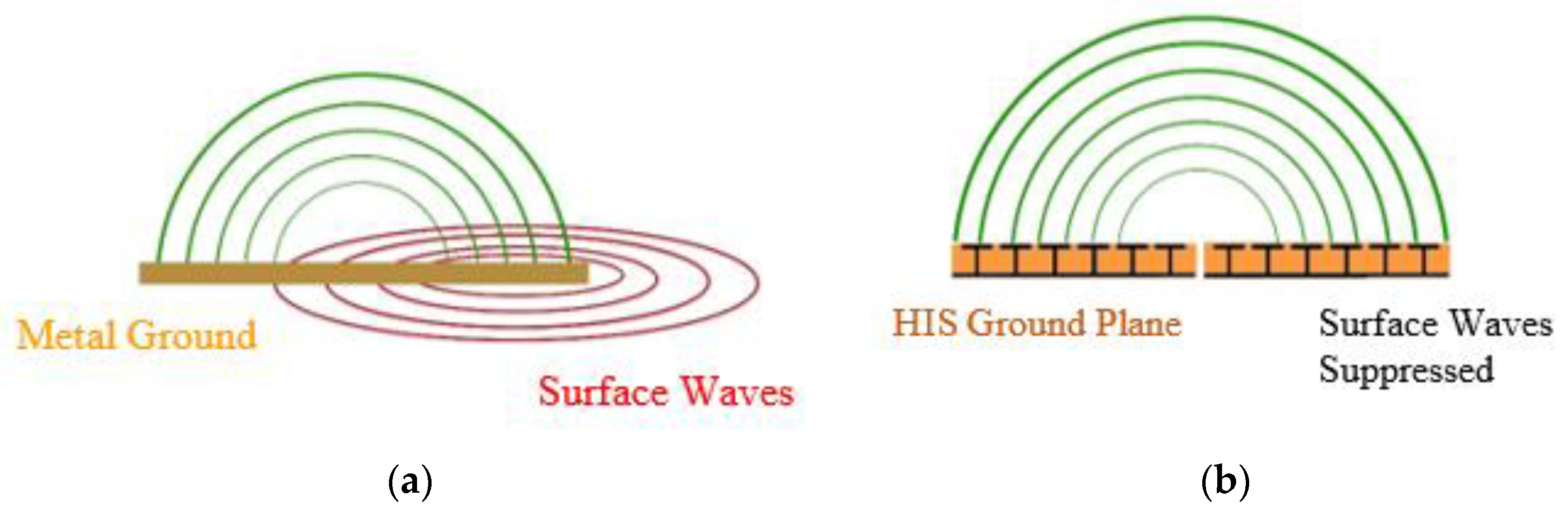
:1. Introduction
2. Design Method
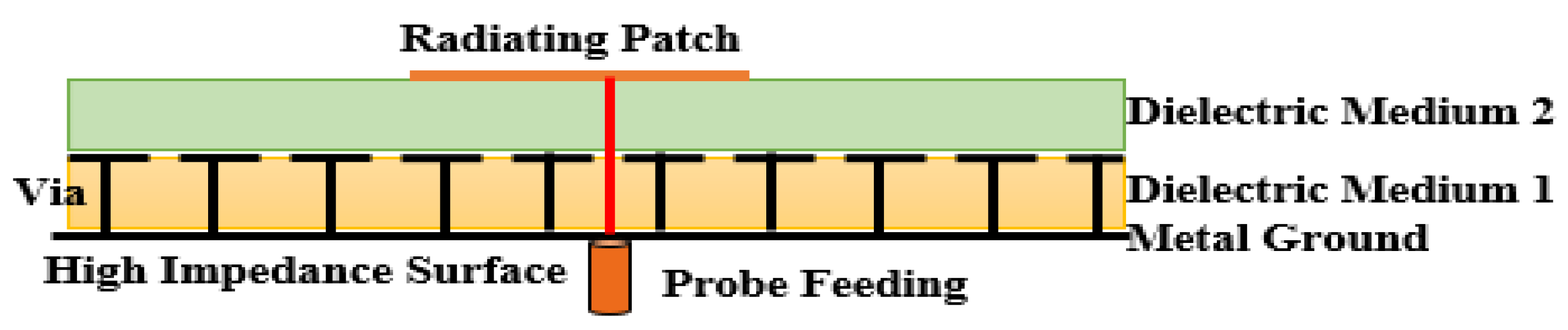
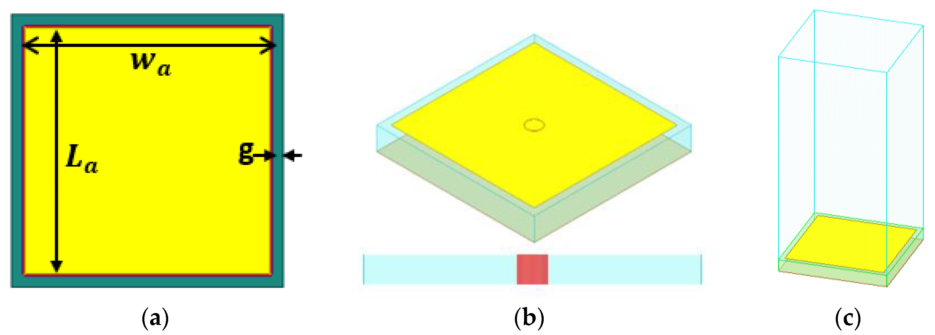
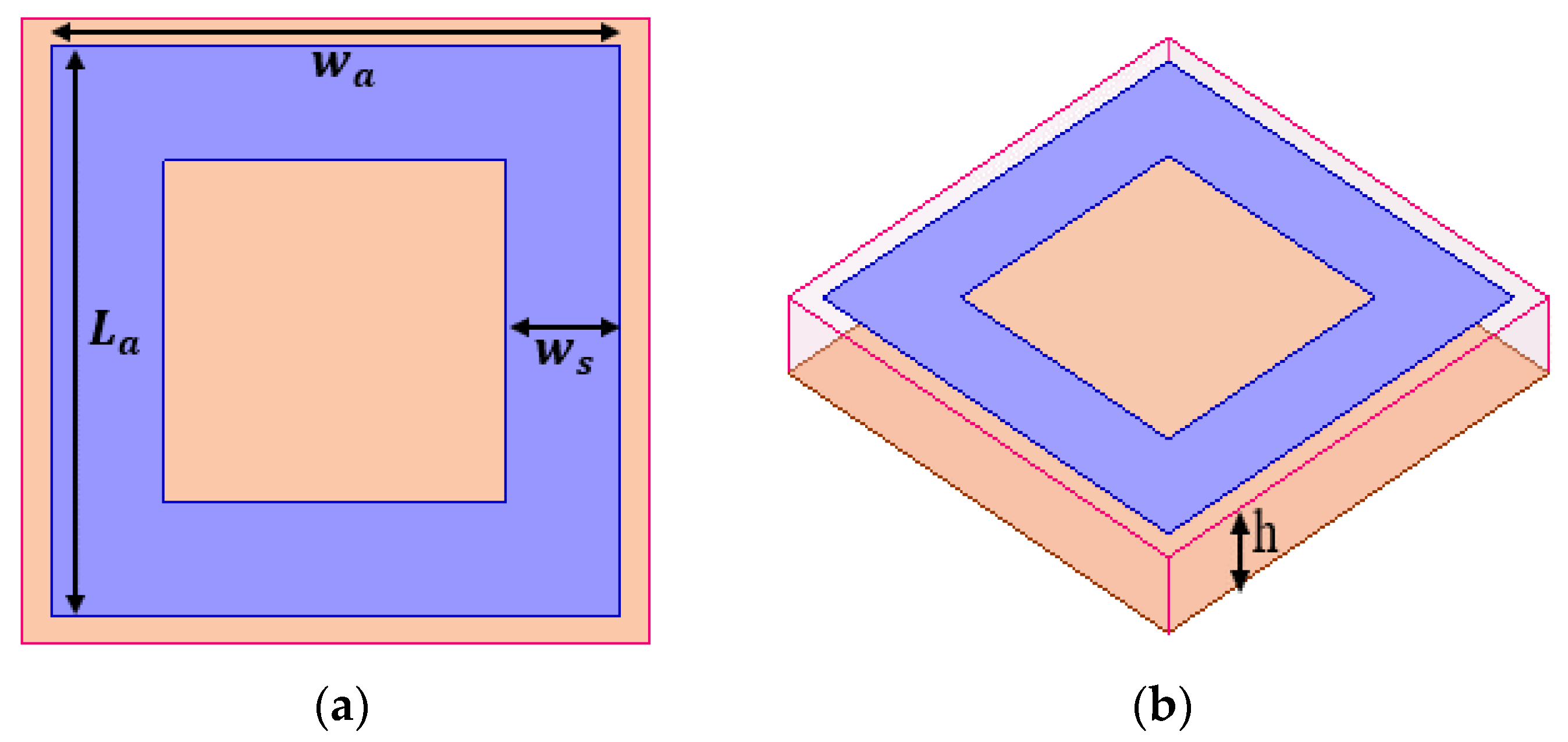
2.1. Conventional Mushroom HIS
2.2. The Slotted Mushroom HIS
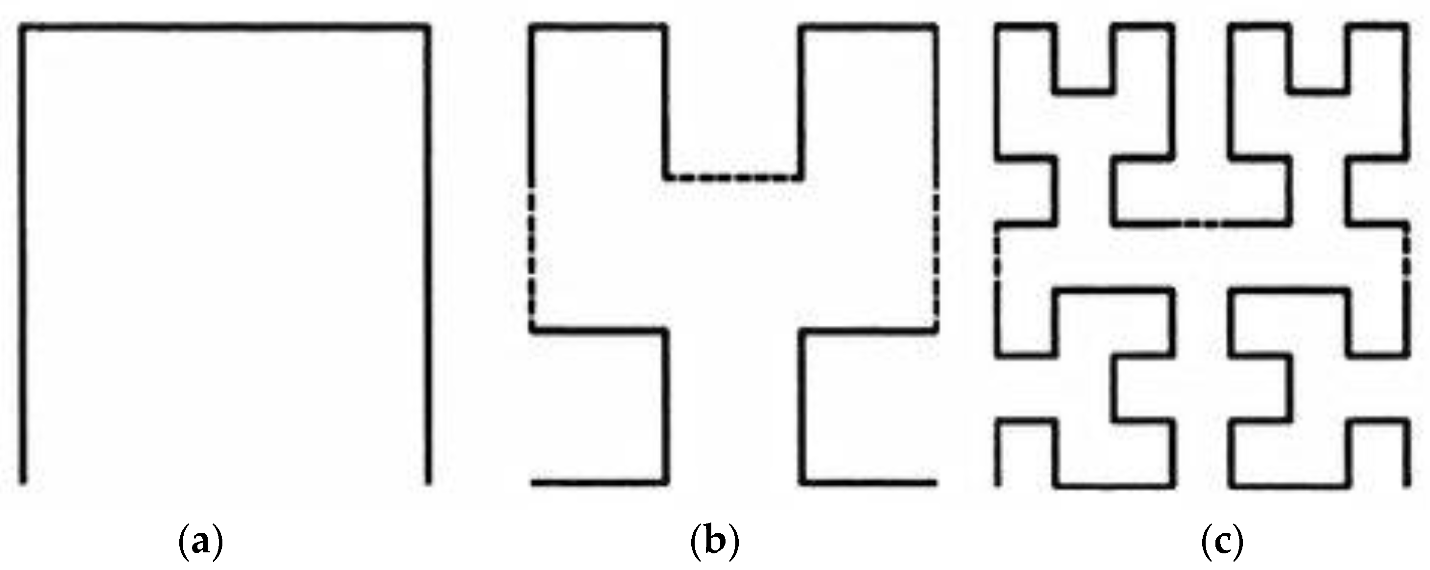
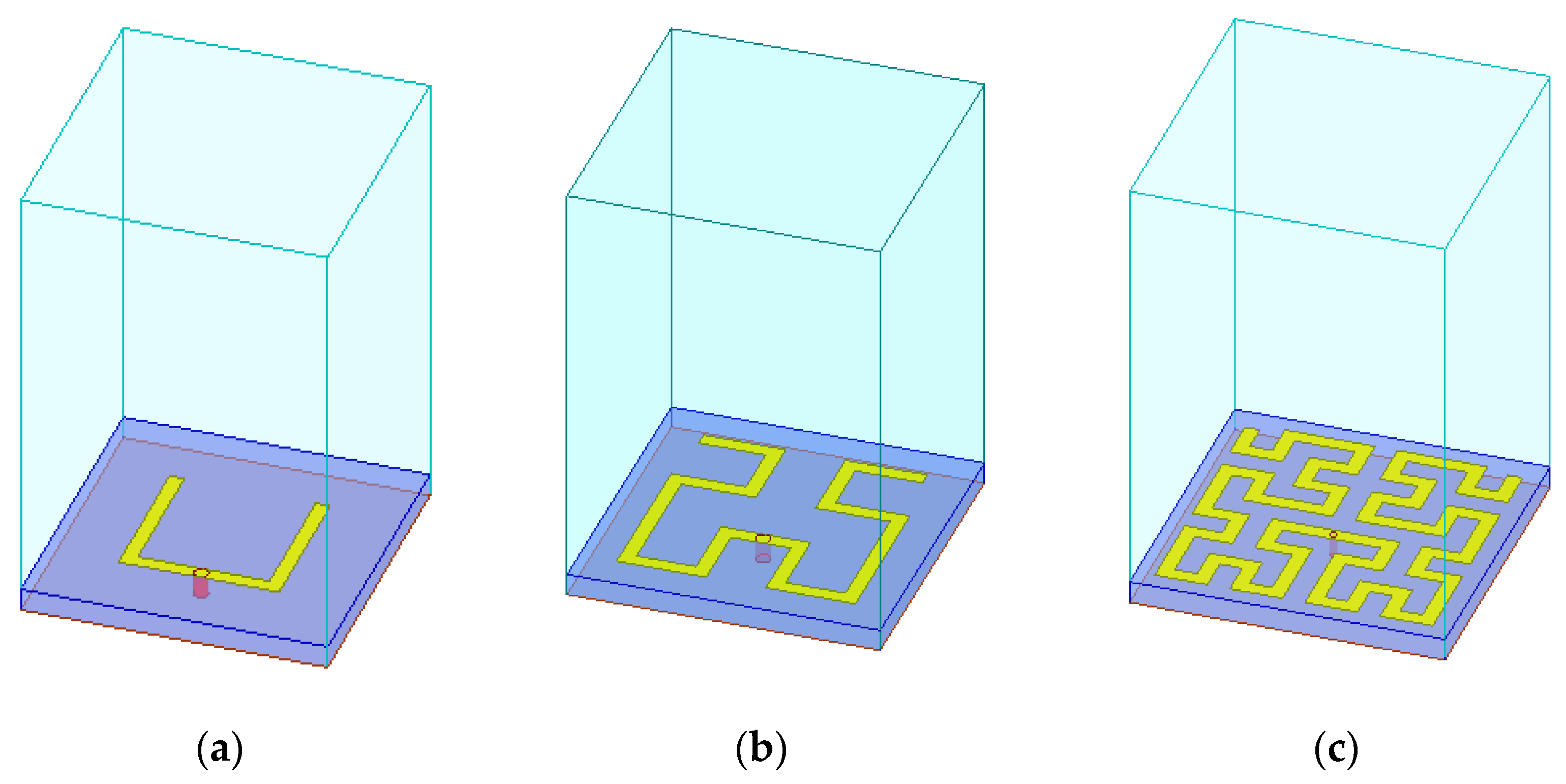
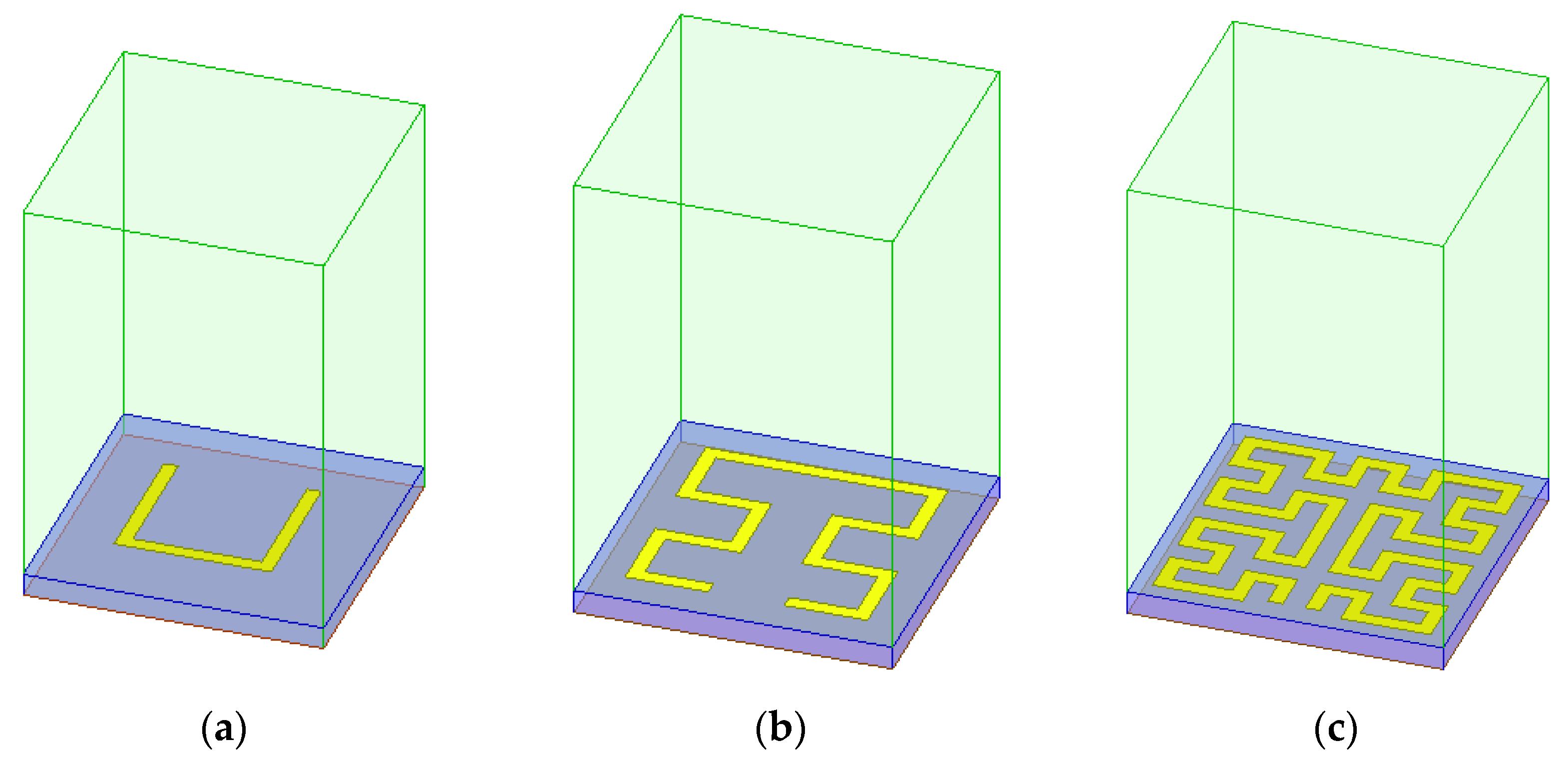
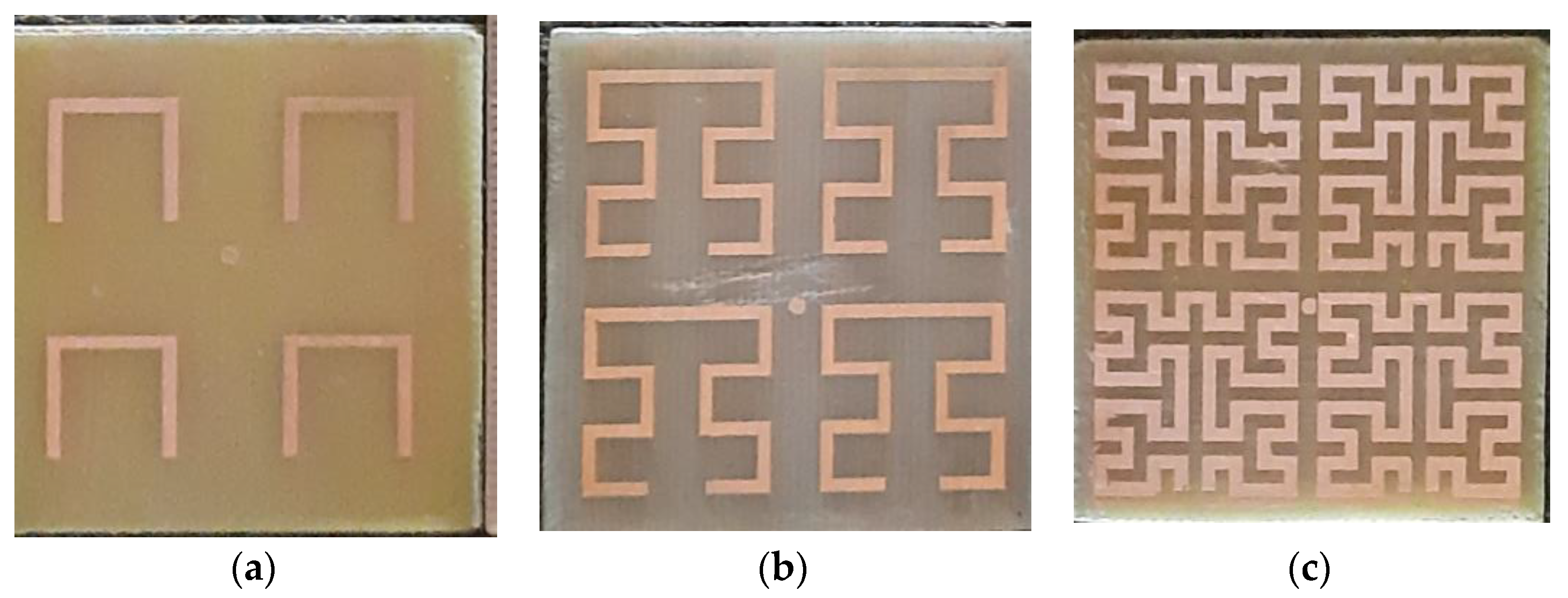
2.3. The Hilbert Curve Fractal HIS
2.4. The Moore Curve Fractal HIS
3. Results and Discussions
3.1. Conventional Mushroom HIS Cell
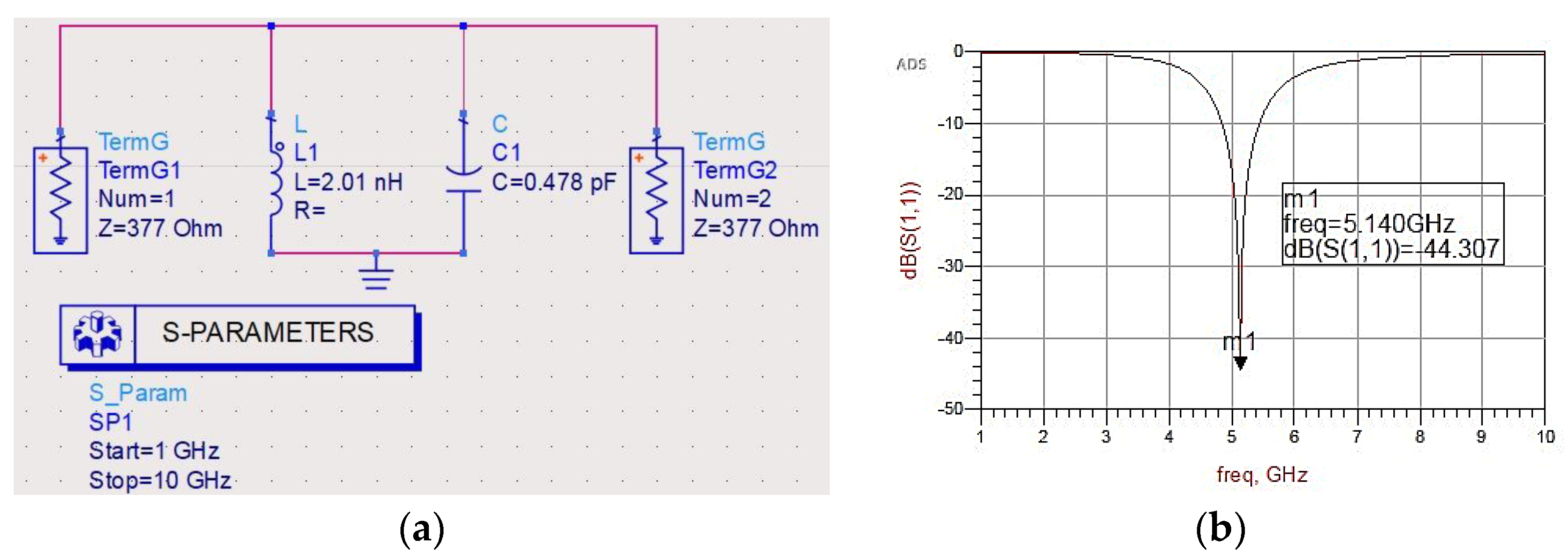
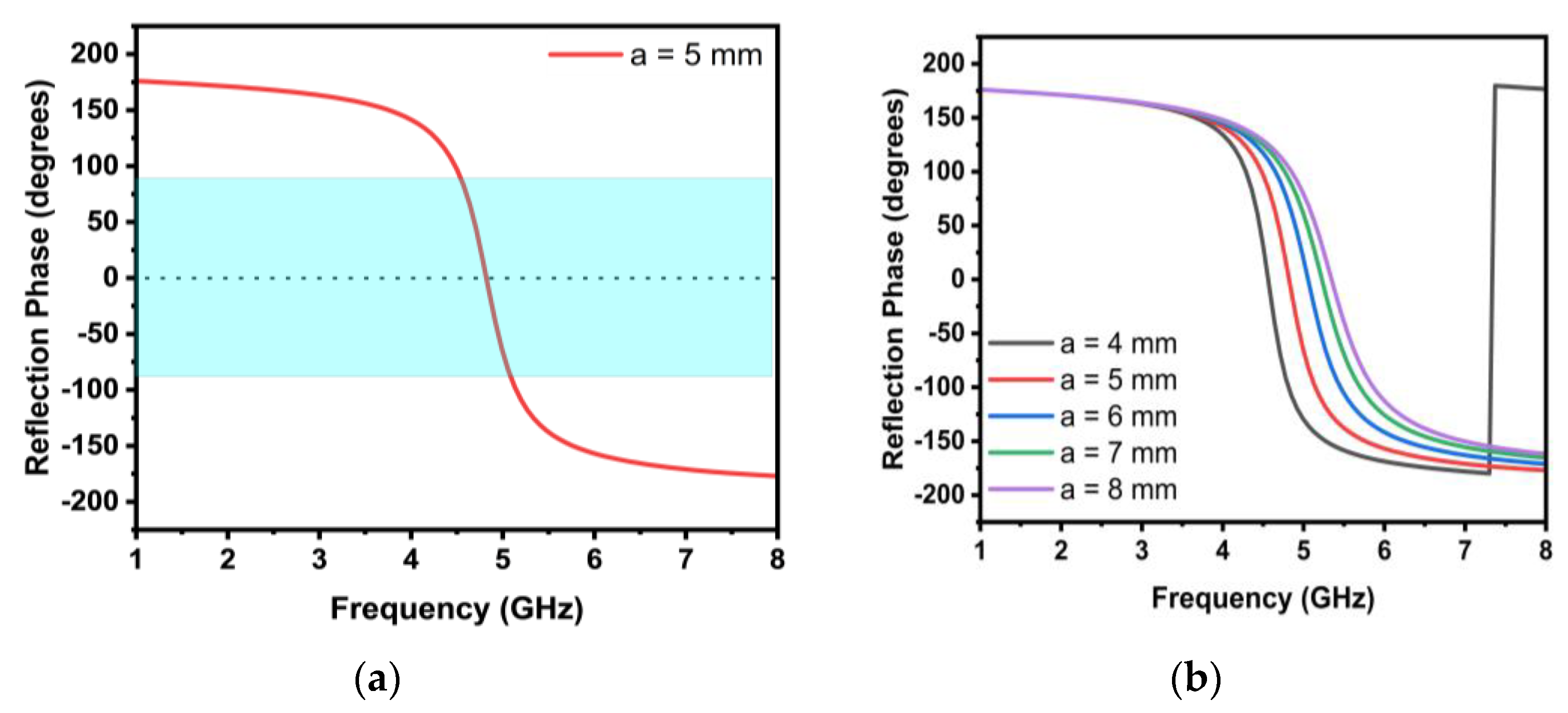
3.1.1. Lumped Circuit Analysis
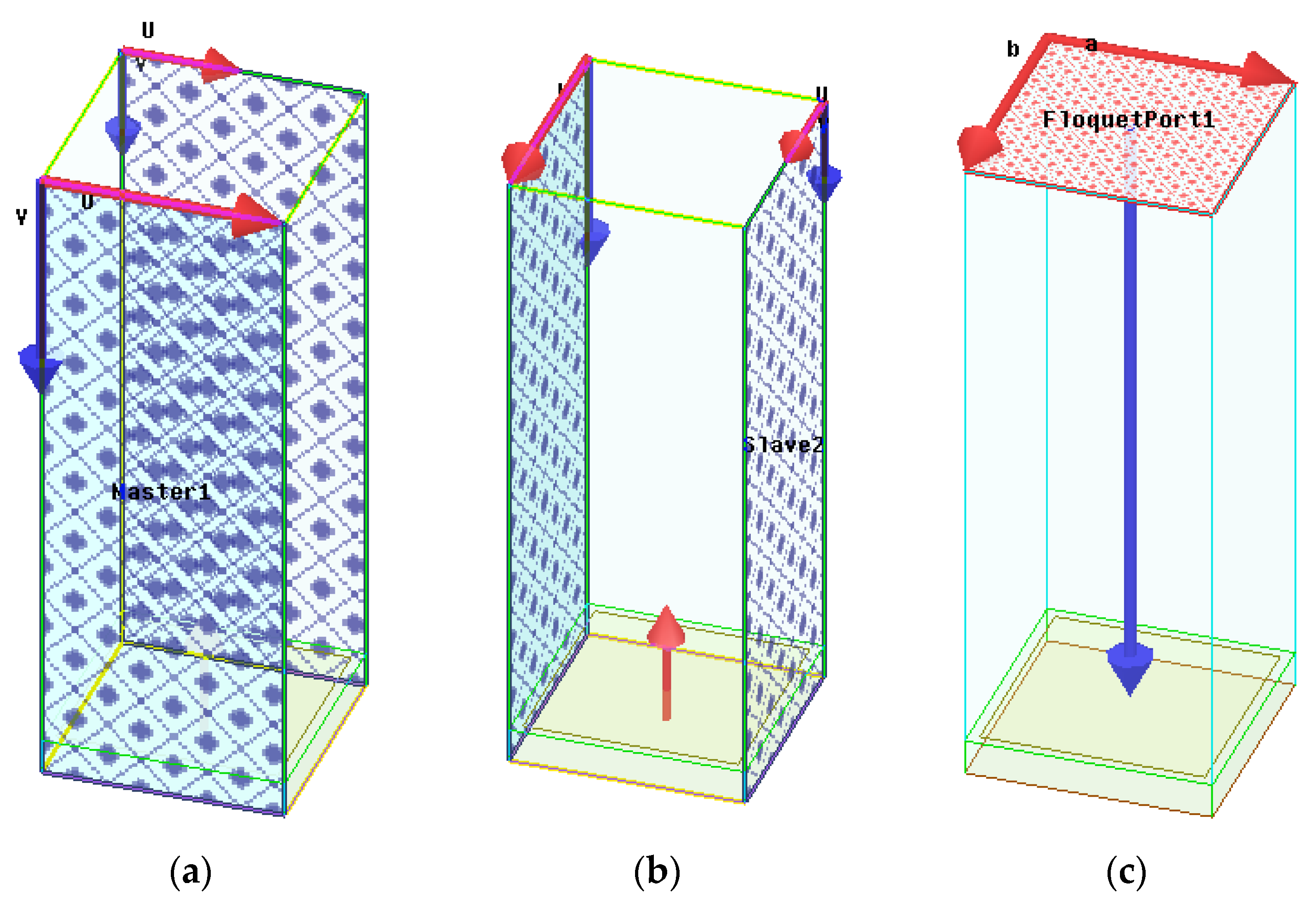
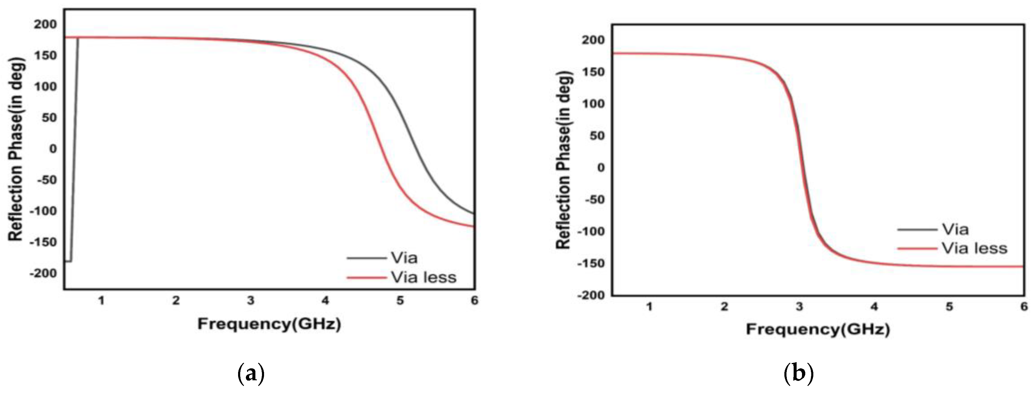
3.1.2. The FDTD Analysis
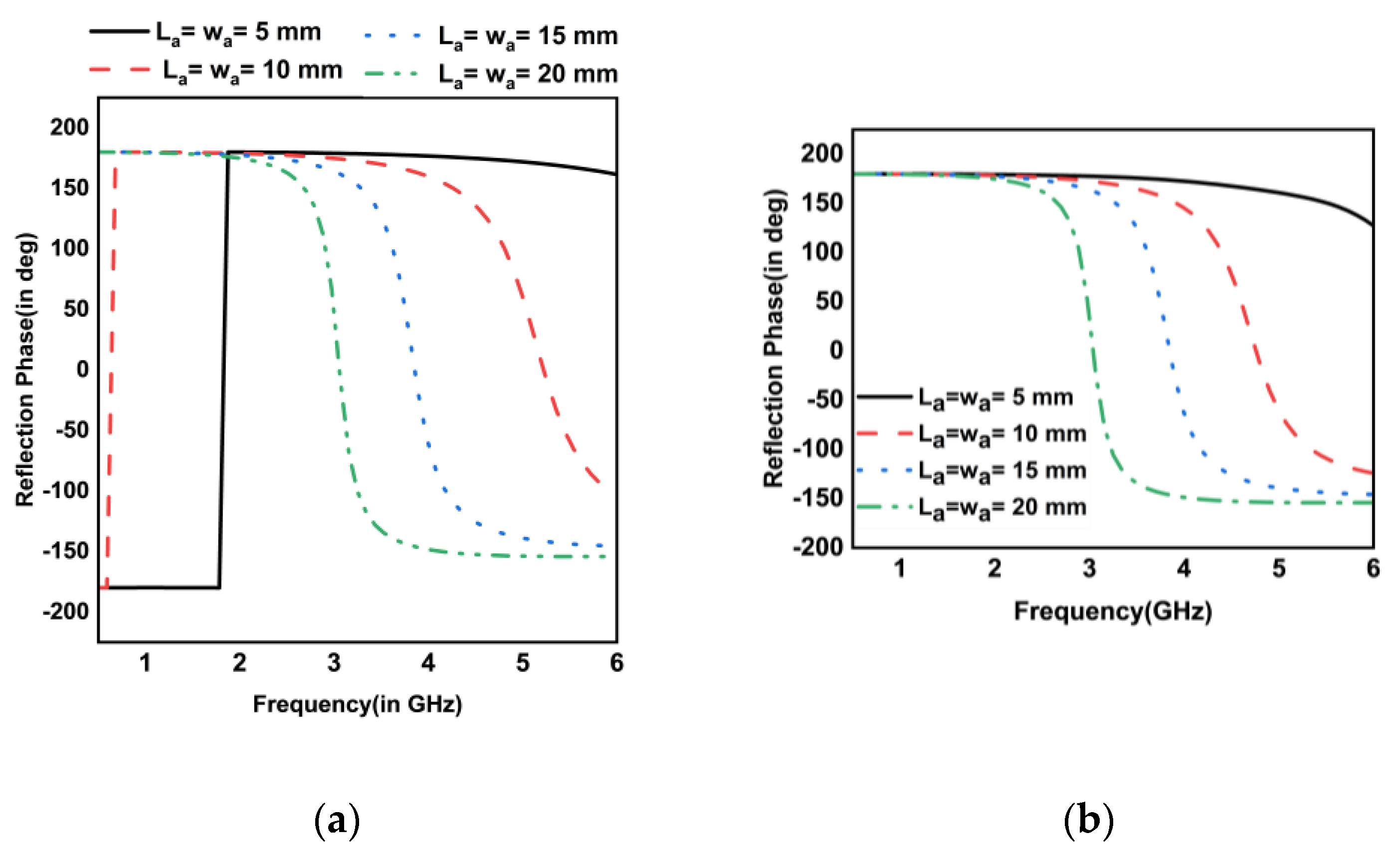
3.2. The Reflection Phase Characteristics of Slotted Mushroom
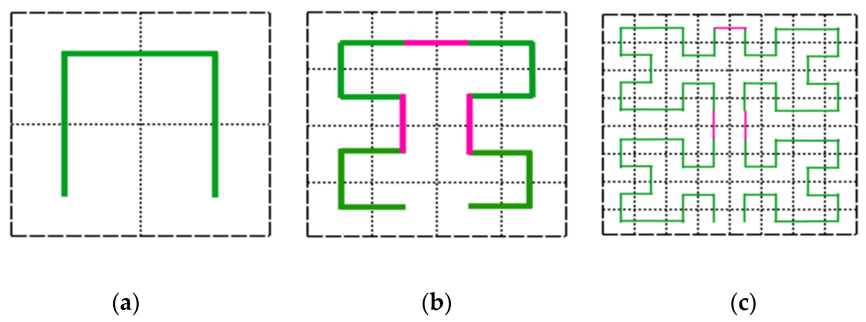
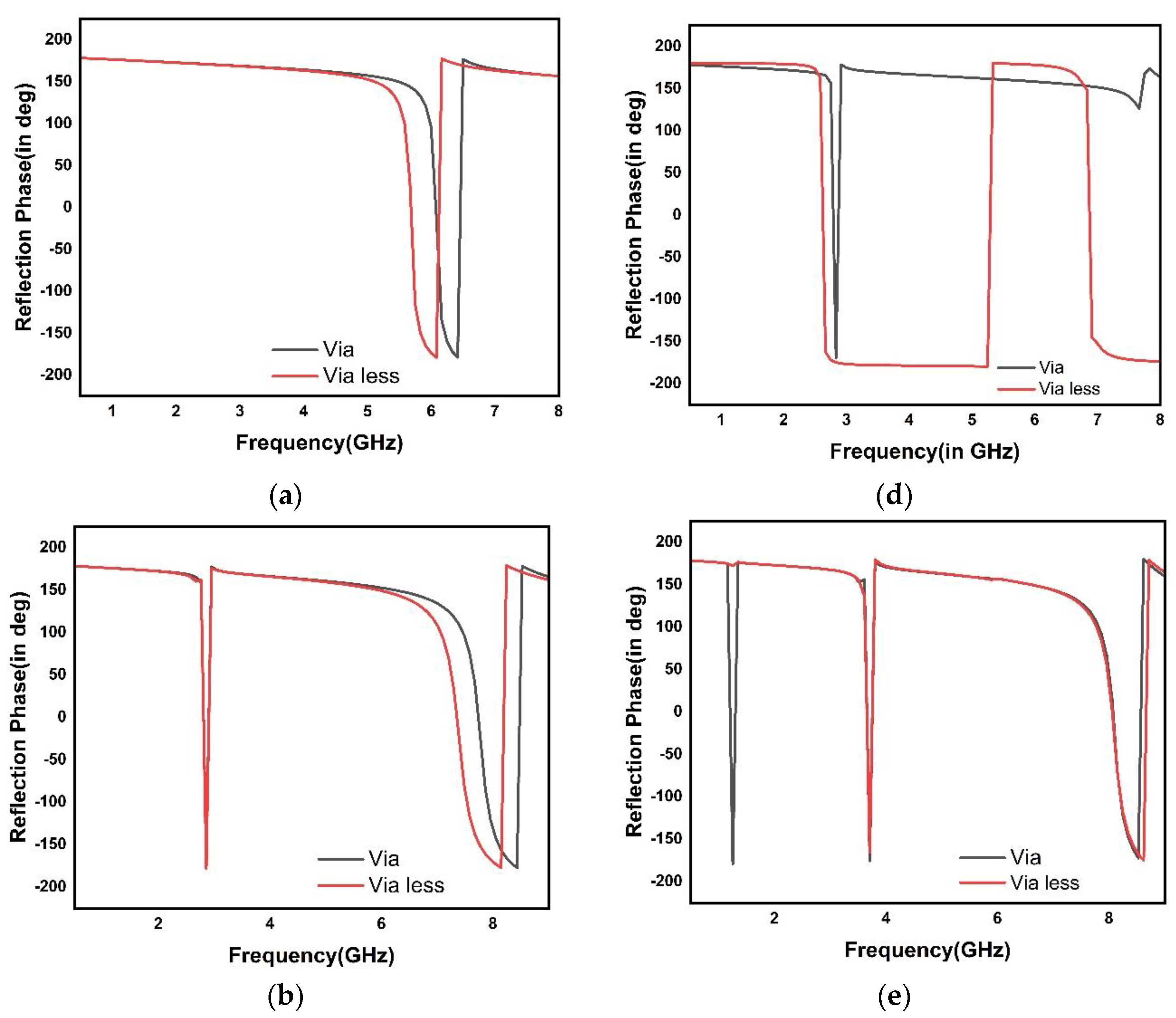
3.3. The Hilbert Curve Fractal HIS Cell
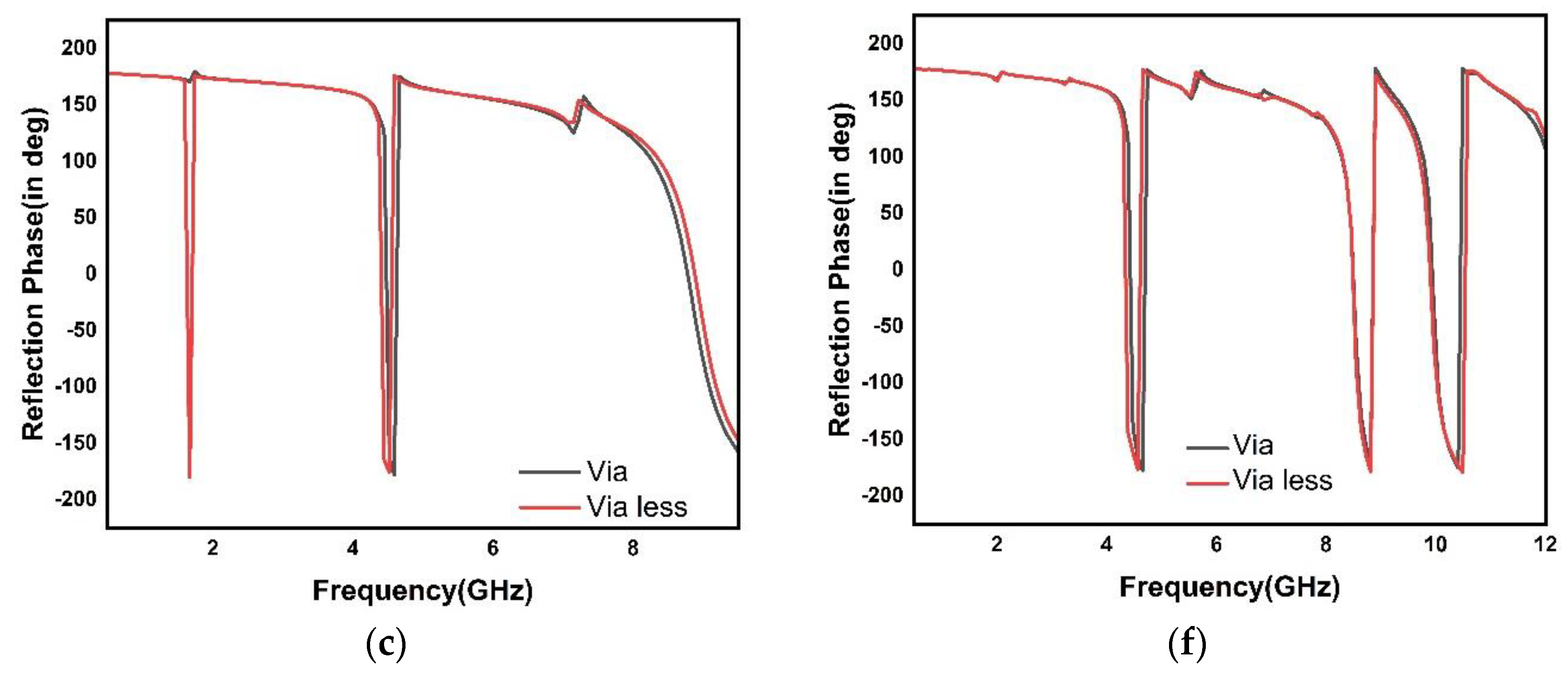
3.4. Moore Curve Fractal HIS
4. Conclusions
Author Contributions
Funding
Data Availability Statement
Conflicts of Interest
References
- Sievenpiper, D.; Broas, R.; Yablonovitch, E. Antennas on high-impedance ground planes. In Proceedings of the 1999 IEEE MTT-S International Microwave Symposium Digest (Cat. No.99CH36282), Anaheim, CA, USA, 13–19 June 1999; Volume 3, pp. 1245–1248. [Google Scholar] [CrossRef]
- Sievenpiper, D.; Zhang, L.; Yablonovitch, E. High-impedance electromagnetic ground planes. In Proceedings of the 1999 IEEE MTT-S International Microwave Symposium Digest (Cat. No.99CH36282), Anaheim, CA, USA, 13–19 June 1999; Volume 4, pp. 1529–1532. [Google Scholar] [CrossRef]
- Sievenpiper, D.; Zhang, L.; Broas, R.; Alexopolous, N.; Yablonovitch, E. High-impedance electromagnetic surfaces with a forbidden frequency band. IEEE Trans. Microw. Theory Tech. 1999, 47, 2059–2074. [Google Scholar] [CrossRef] [Green Version]
- Wei, X.C.; Shu, Y.F.; Zhang, J.B.; Wang, D. Applications of high impedance surfaces for surface wave elimination. In Proceedings of the 2016 URSI Asia-Pacific Radio Science Conference (IEEE/URSI AP-RASC), Seoul, Korea, 21–25 August 2016; pp. 1458–1461. [Google Scholar]
- Gu, M.; Vorobiev, D.; Kim, W.S.; Chien, H.-T.; Woo, H.-M.; Hong, S.C.; Park, S.I. A novel approach using an inductive loading to lower the resonant frequency of a mushroom-shaped high impedance surface. Prog. Electromagn. Res. M 2020, 90, 19–26. [Google Scholar] [CrossRef] [Green Version]
- Broas, R.; Sievenpiper, D.; Yablonovitch, E. A high-impedance ground plane applied to a cellphone handset geometry. IEEE Trans. Microw. Theory Tech. 2001, 49, 1262–1265. [Google Scholar] [CrossRef]
- Yang, F.; Rahmat-Samii, Y. Reflection phase characterizations of the EBG ground plane for low profile wire antenna applications. IEEE Trans. Antennas Propag. 2003, 51, 2691–2703. [Google Scholar] [CrossRef] [Green Version]
- Costa, F.; Luukkonen, O.; Simovski, C.R.; Monorchio, A.; Tretyakov, S.A.; de Maagt, P.M. TE surface wave resonances on high-impedance surface based antennas: Analysis and modelling. IEEE Trans. Antennas Propag. 2011, 59, 3588–3596. [Google Scholar] [CrossRef]
- Mcvay, J.; Engheta, N.; Hoorfar, A.; Member, S. High Impedance Metamaterial Surfaces Using Hilbert-Curve Inclusions. IEEE Microw. Wirel. Compon. Lett. 2004, 14, 130–132. [Google Scholar] [CrossRef] [Green Version]
- Mahdi, M.A.; Abdullah, M.K.; Poopalan, P.; Ahmad, H.; Vinoy, K.J.; Jose, K.A.; Varadan, V.K.; Varadan, V.V.; Materials, A. Hilbert curve fractal antenna: A small resonant antenna for VHF/UHF applications. Microw. Opt. Technol. Lett. 2001, 29, 215–219. [Google Scholar]
- Vinoy, K.; Jose, K.; Varadan, V. Hilbert curve fractal antennas with reconfigurable characteristics. In Proceedings of the 2001 IEEE MTT-S International Microwave Symposium Digest (Cat. No. 01CH37157), Phoenix, AZ, USA, 20–24 May 2001; Volume 1, pp. 381–384. [Google Scholar]
- Murad, N.A.; Esa, M.; Yusoff, M.F.; Ali, S.H. Hilbert curve fractal antenna for RFID application. In Proceedings of the 2006 International RF and Microwave Conference, Putra Jaya, Malaysia, 12–14 September 2006; pp. 182–186. [Google Scholar]
- Wang, Y.; Wang, Z.; Li, J. UHF Moore Fractal Antennas for Online GIS PD Detection. IEEE Antennas Wirel. Propag. Lett. 2016, 16, 852–855. [Google Scholar] [CrossRef]
- Chowdary, P.S.R.; Prasad, A.M.; Rao, P.M.; Anguera, J. Design and Performance Study of Sierpinski Fractal Based Patch Antennas for Multiband and Miniaturization Characteristics. Wirel. Pers. Commun. 2015, 83, 1713–1730. [Google Scholar] [CrossRef]
- Anguera, J.; Andújar, A.; Jayasinghe, J.; Chakravarthy, V.V.S.S.S.; Chowdary, P.S.R.; Pijoan, J.L.; Ali, T.; Cattani, C. Fractal Antennas: An Historical Perspective. Fractal Fract. 2020, 4, 3. [Google Scholar] [CrossRef] [Green Version]
- Ali, J.K. A new microstrip-fed printed slot antenna based on Moore space-filling geometry. In Proceedings of the 2009 Loughborough Antennas & Propagation Conference, Loughborough, UK, 16–17 November 2009. [Google Scholar]
- Saraswat, R.K.; Kumar, M. Implementation of hybrid fractal metamaterial inspired frequency band reconfigurable multiband antenna for wireless applications. Int. J. RF Microw. Comput. Eng. 2020, 30, e22315. [Google Scholar] [CrossRef]
- Bangi, I.S.; Sivia, J.S. Minkowski and Hilbert curves based hybrid fractal antenna for wireless applications. AEU Int. J. Electron. Commun. 2018, 85, 159–168. [Google Scholar] [CrossRef]
- Bangi, I.S.; Sivia, J.S. Moore, Minkowski and Koch Curves Based Hybrid Fractal Antenna for Multiband Applications. Wirel. Pers. Commun. 2019, 108, 2435–2448. [Google Scholar] [CrossRef]
- Anguera, J.; Puente, C.; Martinez, E.; Rozan, E. The fractal Hilbert monopole: A two-dimensional wire. Microw. Opt. Technol. Lett. 2003, 36, 102–104. [Google Scholar] [CrossRef]
- Gupta, A.K.; Chowdary, P.S.R.; Krishna, M.V. Design of Rectangular Patch Antenna on the Hilbert Fractal-shaped High Impedance Surface. J. Sci. Ind. Res. 2023, 82, 202–209. [Google Scholar] [CrossRef]
- Gupta, A.K.; Satish Rama Chowdary, P.; Vamshi Krishna, M. High-Impedance Surface Backed Circular Patch Antenna for Wireless Communications. In Computer Communication, Networking and IoT. Lecture Notes in Networks and Systems; Satapathy, S.C., Lin, J.C.W., Wee, L.K., Bhateja, V., Rajesh, T.M., Eds.; Springer: Singapore, 2023; Volume 459. [Google Scholar] [CrossRef]
- Mosallaei, H.; Rahmat-Samii, Y. Broadband Characterization of Complex Periodic EBG Structures: An FDTD/Prony Technique Based on the Split-Field Approach. Electromagnetics 2003, 23, 135–151. [Google Scholar] [CrossRef]
- Yang, F.R.; Marchio, J.; Qian, Y.; Itoh, T. A Novel TEM-Waveguide Using Uniplanar Compact Photonic Band-Gap (UC-PBG) Structure. IEEE Trans. Microwave Theory Tech. 1999, 47, 2092–2098. [Google Scholar] [CrossRef]
- Terlapu, S.K.; Chowdary PS, R.; Jaya, C.; Sameer Chakravarthy VV, S.S.; Satpathy, S.C. On the design of fractal UWB wide-slot antenna with notch band characteristics. In Microelectronics, Electromagnetics and Telecommunications: Proceedings of ICMEET 2017; Springer: Singapore, 2018; pp. 907–912. [Google Scholar]


| Dimension (in mm) | With Via V = 0.5 mm (Frequency in GHz) | Via Less (Frequency in GHz) | ||||
|---|---|---|---|---|---|---|
| 1.83 | 1.81 | 1.85 | — | — | — | |
| 0.64 | 0.61 | 0.66 | — | — | — | |
| 5.22 | 4.86 | 5.77 | 4.76 | 4.45 | 5.22 | |
| 3.85 | 3.65 | 4.12 | 3.85 | 3.65 | 4.12 | |
| 3.06 | 2.93 | 3.22 | 3.04 | 2.91 | 3.20 | |
| Ring Width (in mm) | 0° Frequency (in GHz) | Frequency (in GHz) | Frequency (in GHz) | Bandwidth (in GHz) |
|---|---|---|---|---|
| 4 | 4.56 | 4.33 | 4.78 | 0.45 |
| 5 | 4.82 | 4.54 | 5.10 | 0.56 |
| 6 | 5.06 | 4.72 | 5.39 | 0.67 |
| 7 | 5.23 | 4.84 | 5.62 | 0.78 |
| 8 | 5.35 | 4.93 | 5.76 | 0.83 |
| Dimension (in mm) | With Via Radius V = 0.5 mm (Frequency in GHz) | Via Less (Frequency in GHz) | ||||
|---|---|---|---|---|---|---|
| HILF10_1 | 6.07 | 6.00 | 6.14 | 5.69 | 5.6 | 5.74 |
| HILF10_2 | 2.81 | 2.79 | 2.84 | 2.81 | 2.79 | 2.84 |
| 7.74 | 7.52 | 7.88 | 7.35 | 7.12 | 7.51 | |
| HILF10_3 | — | — | — | 1.63 | 1.61 | 1.65 |
| 4.48 | 4.46 | 4.50 | 4.41 | 4.38 | 4.43 | |
| 8.78 | 8.37 | 9.05 | 8.88 | 8.48 | 9.15 | |
| Dimension (in mm) | With Via Radius V = 0.5 mm (Frequency in GHz) | Via Less (Frequency in GHz) | ||||
|---|---|---|---|---|---|---|
| HILF20_1 | 2.79 | 2.77 | 2.81 | 2.63 | 2.60 | 2.65 |
| HILF20_2 | 1.21 | 1.18 | 1.23 | — | — | — |
| 3.66 | 3.64 | 3.69 | 3.66 | 3.63 | 3.69 | |
| 8.07 | 7.87 | 8.19 | 8.06 | 7.83 | 8.19 | |
| HILF20_3 | 4.43 | 4.40 | 4.46 | 4.35 | 4.32 | 4.37 |
| 8.49 | 8.33 | 8.58 | 8.49 | 8.34 | 8.55 | |
| 9.93 | 9.80 | 10.03 | 9.90 | 9.73 | 10.01 | |
| Dimension (in mm) | With Via V = 0.5 mm (Frequency in GHz) | Via Less (Frequency in GHz) | ||||
|---|---|---|---|---|---|---|
| MooreF10_1 | 6.09 | 6.00 | 6.10 | 5.51 | 5.43 | 5.52 |
| MooreF10_2 | 2.81 | 2.80 | 2.81 | 2.81 | 2.80 | 2.81 |
| 7.74 | 7.74 | 7.75 | — | — | — | |
| MooreF10_3 | 6.80 | 6.68 | 6.85 | 6.95 | 6.70 | 7.10 |
| 8.45 | 8.17 | 8.74 | 8.44 | 8.17 | 8.76 | |
| Dimension (in mm) | With Via V = 0.5 mm (Frequency in GHz) | Via Less (Frequency in GHz) | ||||
|---|---|---|---|---|---|---|
| MooreF20_1 | — | — | — | 2.91 | 2.90 | 2.92 |
| MooreF20_2 | 5.85 | 5.80 | 5.86 | 5.89 | 5.82 | 5.91 |
| 7.98 | 7.75 | 8.11 | 7.92 | 7.7 | 8.08 | |
| 9.78 | 9.63 | 9.93 | 9.68 | 9.55 | 9.83 | |
| MooreF20_3 | 3.35 | 3.34 | 3.35 | 3.33 | 3.33 | 3.38 |
| 4.40 | 4.35 | 4.45 | 4.41 | 4.35 | 4.45 | |
| 5.87 | 5.85 | 5.87 | 5.85 | 5.83 | 5.86 | |
| 10.01 | 9.98 | 10.16 | 9.97 | 9.93 | 9.98 | |
Disclaimer/Publisher’s Note: The statements, opinions and data contained in all publications are solely those of the individual author(s) and contributor(s) and not of MDPI and/or the editor(s). MDPI and/or the editor(s) disclaim responsibility for any injury to people or property resulting from any ideas, methods, instructions or products referred to in the content. |
© 2023 by the authors. Licensee MDPI, Basel, Switzerland. This article is an open access article distributed under the terms and conditions of the Creative Commons Attribution (CC BY) license (https://creativecommons.org/licenses/by/4.0/).
Share and Cite
Gupta, A.K.; Mohanta, H.C.; Chowdary, P.S.R.; Krishna, M.V.; Mohamed, H.G. Design and Analysis of Fractal-Shaped High-Impedance Surface Unit Cell Characteristics. Fractal Fract. 2023, 7, 472. https://doi.org/10.3390/fractalfract7060472
Gupta AK, Mohanta HC, Chowdary PSR, Krishna MV, Mohamed HG. Design and Analysis of Fractal-Shaped High-Impedance Surface Unit Cell Characteristics. Fractal and Fractional. 2023; 7(6):472. https://doi.org/10.3390/fractalfract7060472
Chicago/Turabian StyleGupta, Akash Kumar, Harish Chandra Mohanta, P. Satish Rama Chowdary, M. Vamshi Krishna, and Heba G. Mohamed. 2023. "Design and Analysis of Fractal-Shaped High-Impedance Surface Unit Cell Characteristics" Fractal and Fractional 7, no. 6: 472. https://doi.org/10.3390/fractalfract7060472