
Metal–Insulator Transition in Doped Barium Plumbates
by
 , ,
, ,
Andreza M. Eufrasio
1,*, 
Ian Pegg
1,
Amrit Kafle
1,
Winnie Wong-Ng
2,
Qingzhen Huang
2 and
Biprodas Dutta
1 1
Vitreous State Laboratory, The Catholic University of America, 620 Michigan Ave N.E., Washington, DC 20064, USA
2
National Institute of Standard and Technology (NIST), Gaithersburg, MD 20899, USA
*
Author to whom correspondence should be addressed.
Electron. Mater. 2021, 2(3), 428-444; https://doi.org/10.3390/electronicmat2030029
Submission received: 14 July 2021
/
Revised: 27 August 2021
/
Accepted: 31 August 2021
/
Published: 16 September 2021
(This article belongs to the Special Issue Feature Papers of Electronic Materials)
Abstract
:Solid solutions in the Ba(Pb1−xSrx)O3−z system were prepared by aliovalent substitution of Pb4+ by Sr2+ ions to investigate the effect of cation stoichiometry on thermal and electrical properties as x was varied between 0 and 0.4, in the temperature range 300–523 K. The starting compound, barium plumbate (BaPbO3), has a perovskite structure and is known to exhibit metallic conductivity due to an overlap of the O2p nonbonding and the Pb–O spσ antibonding band, which is partially filled by the available electrons. The large difference in the ionic radii between the Pb4+ and Sr2+ ions introduces significant strain into the (Pb/Sr)O6 octahedra of the perovskite structure. Additionally, charged defects are created on account of the different oxidation states of the Pb4+ and Sr2+ ions. Evidence of a metal to insulator transition (MIT) of the Mott–Hubbard type has been observed at a critical concentration of Sr2+ ions.
1. Introduction
The Ba (Pb1−xMx)O3−z compounds, where M is either a homo- or an alio-valent cation, are examples of metallic oxides with a perovskite structure that form a large family that displays a wide variety of properties such as superconductivity, ferroelectricity, catalysis, etc. Employing a wide range of cationic substitutions, this system has been investigated for various end uses such as possible cathodes in solid oxide fuels cells, prospective thermoelectric components, and new superconductors [1,2,3,4,5,6,7,8,9,10,11,12,13].
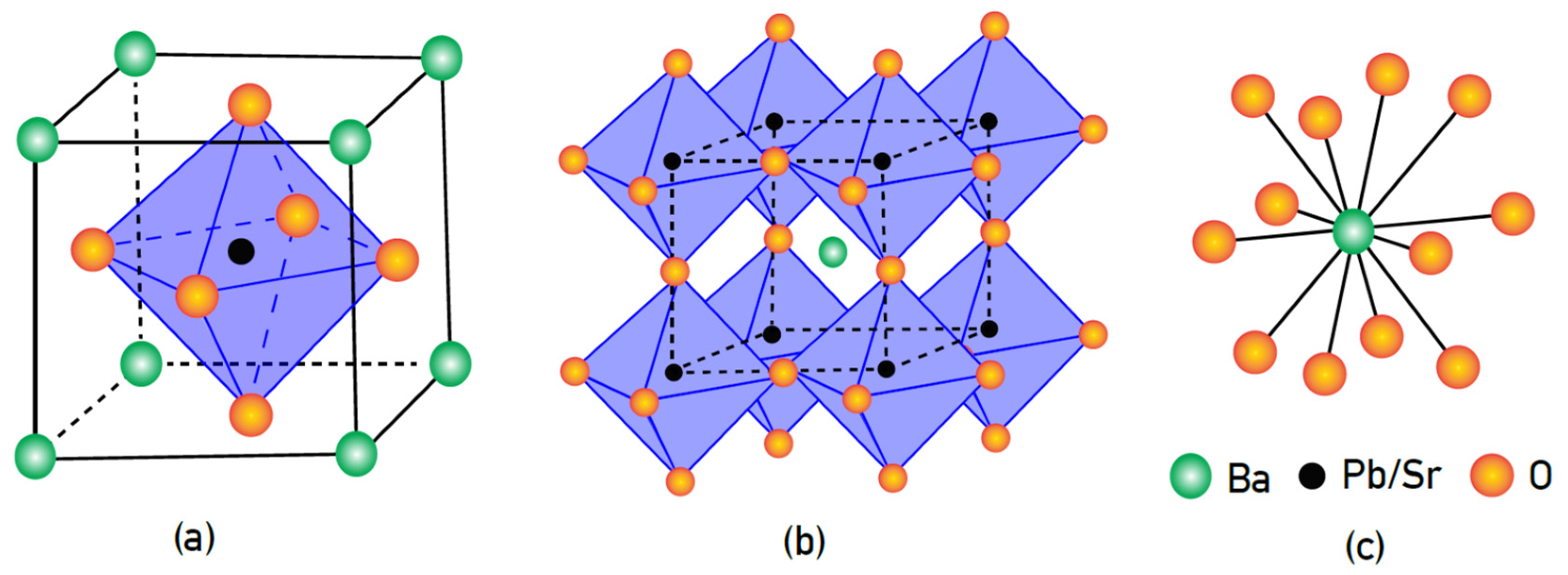
Perovskites assume the general formula ABX3, where A and B are metal ions and X is an anion, normally oxygen. In BaPbO3 the ‘A’ and ‘B’ positions are occupied by Ba and Pb, respectively, as shown in Figure 1a. The sum of the charges on the A and B ions is equal to six, which can be achieved by several means: e.g., A3+B3+ or A2+B4+ (as in the case of BaPbO3). Mixed oxide perovskites [4,5,6,7,8] are also a possibility, e.g., A (B0.5B′0.5)O3, as in Ba (Pb1−xSrx)O3−z (Figure 1b). Certain perovskite oxides, such as BaBiO3 have a cubic crystal structure with upright BX6 octahedra [4]. In these materials, the B cations may be vertically displaced along the octahedral diagonals by suitable cation substitutions without disrupting the original crystal symmetry. Among perovskite compounds, lead is an interesting cation because it can form compounds where it may occupy either site A (large cation) or site B (small cation) [3,4,5]. Depending on the choice of cation, the tilt of the octahedra can be varied, resulting in variation of the properties of the resultant crystal structure [8].
BaPbO3 has a perovskite crystal structure that is orthorhombically distorted with the PbO6 octahedra maintaining a tilt around the [110] direction [6]. The crystal structure of BaPbO3 comprises a close-packed array of Ba2+ and O2− ions where the coordination of oxygen ions around Ba2+ is depicted in Figure 1a,c. The Pb4+ ions, having much smaller dimensions as compared to Ba2+, occupy the octahedral sites formed by O2− ions. The other octahedral sites are not suitable for Ba2+ to occupy because of the smaller volumes of such sites. Some of these sites are unsuitable for even Pb4+ because of the Coulomb repulsion encountered against neighboring Ba2+ ions. Hence, point defects forms of the Frenkel type are unlikely to form in this system [5] and undoped BaPbO3 is more susceptible to act as an acceptor for impurities as defects, as reported in BaTiO3 and SrTiO3 [5]. Moreover, the mobile holes in the valence band (from acceptor ions) can always recombine with the electrons of the Pb-6s and O-2p orbitals and reduce their concentration at the Fermi level of BaPbO3. Hence, the extent of SrO doping should determine the transport properties (electrical conductivity and thermopower) of Ba(Pb1−xSrx)O3−z.
The structure and properties of doped BaPbO3 compounds have long been of interest [1,2,3,4,5,6,7,8,9,10,11,12,13,14,15,16], and even more so after the demonstration of superconductivity in Ba(Pb1−xMx)O3−z, where M is either a homo- or an alio-valent cation. The 3.5 K and 13 K superconductors in the Ba(Pb1−xSbx)O3 [10] and Ba(Pb1−xBix)O3 [8,11] systems, respectively, are examples of such compositions that have been studied extensively. Superconductivity was also discovered when barium was substituted by potassium in Ba0.6K0.4BiO3 (another perovskite), resulting in a superconducting transition, Tc, at 30 K [8,12]. In other words, substitution of both the A and B cations in perovskite compounds exhibited quantum transitions from metallic to superconducting states. As a matter of fact, the discovery of superconductivity in Ba(Pb0.75Bi0.25)O3 was made before high-temperature superconductors (HTSC) came to be known in compounds containing copper oxide [8]. The crystal structures of the copper oxide based HTSCs and the Ba–(Pb/Bi)–O system have quite a few similarities: (i) both the systems crystallize as perovskites and (ii) the CuOn or the (Bi/Pb)O6 octahedra share common oxygen ions. Strong hybridization of the covalent (Pb/Bi)-6s/Cu-3d-O 2pσ bonds and the highly anharmonic oxygen-ion vibration [7,8,12] are inherent to the CuO-based HTSCs as well as to the Ba(Pb1−xMx)O3−z and (Ba1−xKx)BiO3 superconducting oxides. In the Ba(Pb1−xCux)O3−z system, however, a metal (conductor) to insulator transition (MIT) [17,18,19,20] has been reported by Kodenkandath [7] at x = 0.35, where the itinerant behavior of the electrons changes to one that is localized at x ≥ 0.35, whereas in a metal, the charge carriers (electrons/holes) have negligible interaction with the surrounding lattice, the situation changes when MIT sets in. In the insulating state, the carriers are localized, and it is established that such carriers always deform the surrounding lattice [8,20]. The pseudoparticles formed by the carriers and the associated lattice deformations are known as polarons. Strong electron-phonon interactions leading to the formation of polarons are facilitated at high temperatures (>θ/3, where θ is the Debye temperature). The dimensions of such pseudoparticles are calculated using a simple equation adopted by Mott [20] and also by Greaves [21]. Conduction in such polaronic systems is described by the transport of the carriers along with the associated lattice deformation. The mobility of polarons is typically lower than that of itinerant electrons.
Band structure calculations have shown [13,14,15] that the metallic conductivity exhibited by BaPbO3 is a result of the overlap of the Pb-6s and O-2p orbitals at the Fermi level (EF). This band is only partially occupied by the available electrons and, therefore, BaPbO3 exhibits metallic conductivity. A report by Fu [6], on the other hand, has demonstrated that a shortened Pb–O distance in the oxygen octahedra affects the interaction of the Pb-6s and O-2p electrons differently. Instead of giving a half-filled metallic band, it actually results in the formation of a band gap. In the present investigation, aliovalent substitution of PbO by equimolar SrO was carried out in the Ba(Pb1−xSrx)O3−z system to explore if a quantum phase change (superconductivity or MIT) occurs at a certain dopant level as reported earlier in similar perovskite systems [7,8]. The interest in using SrO, a known acceptor [5], as the dopant was to investigate the relationship of structure and electrical/thermal properties as the density of charge carriers was systematically decreased with increasing x.
The cation substitutions in the present investigation using metallic BaPbO3 as the starting compound was planned with an intention of introducing simultaneous size and charge mismatch in the perovskite structure. Compared to the ionic radius of Pb4+ (0.78 Å) in octahedral coordination, the ionic radius of Sr2+ in octahedral coordination is 1.18 Å, which introduces a ~50% size mismatch. The rationale behind this large size mismatch was an attempt to distort the oxygen tetrahedra surrounding the B atoms of the perovskite crystal [7,8]. As the Pb–O and Sr–O bond lengths were expected to be different, substitution of Pb by Sr ions was expected to alter the tilt of the oxygen octahedra. In the (Ba1−xKx)BiO3 system, such tilting of the BiO6 octahedra by the substitution of Ba by K ions was found to be instrumental in triggering MIT at x > 0.37. When x is further increased to 0.40, (Ba1−xKx)BiO3 exhibited superconductivity [8]. The present investigation has demonstrated that despite the charge and size difference, partial substitution of Pb4+ by Sr2+ (up to x = 0.4) was possible without the precipitation of a second phase. It has also been shown by Xin et al. [5] that substitution of a Pb4+ with a lower valence cation, Sr2+ in the present investigation, introduces two holes. Hence, electron concentration at the Fermi level was expected to decrease as a result of partial substitution of PbO by SrO as a result of recombination of such holes by the itinerant electrons. In this paper, we report a quantum transition from metallic to an insulating phase at a critical concentration of Sr2+ ions in the Ba(Pb1−xSrx)O3−z system.
2. Materials and Methods
2.1. Sample Preparation
Polycrystalline samples of Ba(Pb1−xSrx)O3−z for x = 0.0, 0.1, 0.2, 0.3, and 0.4 were prepared using stoichiometric proportions of reagent grade BaO, PbO2, and SrO and the compositions are listed in Table 1. A mini-bead beater was employed to mix the powdered ingredients after manually mixing them in a mortar and pestle.
Several identical pellets of each composition were prepared using the procedure described above. One such pellet would be ground to powder for X-ray fluorescence (XRF) (Axios, Panalytical, Almelo, The Netherlands) analysis for confirmation of sample composition as listed in Table 1. The XRF composition was accurate to about 10% of the nominal composition used. The same powder would then be used for X-ray and Neutron powder diffraction analyses.
2.2. Density Measurement
Density measurements were performed using a specific gravity method utilizing standard pycnometers using deionized water. Appropriate temperature corrections were applied. The error in density measurements is estimated at ±0.01 g/cm3 and the latter are listed in Table 1.
2.3. Scanning Electron Microscope (Sem) Analysis
For each composition, 13 mm dia pellets as well as crushed powder were mounted on separate aluminum stubs with conductive carbon tape and coated with carbon for SEM analyses. SEM analyses were carried out using a combination of photomicrography and energy dispersive X-ray spectroscopy (EDS). Image acquisition was carried out on a JEOL-5910 SEM (JEOL, Austin, TX, USA). For each sample, photomicrographs were acquired at high resolution and magnification (up to 15,000×, 4 kV, 35 nm spot size) to analyze the microstructure. In addition, elemental analyses were performed using an Oxford Instruments INCA–X-Sight EDS detector (Oxford Instruments, Los Angeles, CA, USA) to determine the homogeneity and phase compositions of the samples.
2.4. X-ray Diffraction (Xrd) Analysis
X-ray diffraction (XRD) analyses (Thermo ARL, Ecublens, Switzerland) were conducted on powdered specimens to determine the crystalline phases using a Thermo ARLX’TRA diffractometer with CuKα radiation (λ = 0.1541 nm). The XRD scans were performed between 2θ values of 10° and 70° with spacing of 0.02° between data points and a collection time of 4 s provided for each data point. Analyses of XRD patterns were performed using Jade 9 software in search-match mode to identify the phases.
2.5. Neutron Powder Diffraction Analysis
Neutron powder diffraction data for Ba(Pb1−xSrx)O3−z were collected at the NIST Center for Neutron Research on the high resolution neutron powder diffractometer (BT–1) with neutrons of wavelength 1.5397 Å produced by using a Cu(311) monochromator. Collimators with horizontal divergences of 60′, 20′, and 7′ of arc were used before and after the monochromator and the sample, respectively. Data were collected at room temperature in the 2θ range of 3–168° with a step size of 0.05°. The structural parameters, both nuclear and magnetic, were determined by Rietveld refinement of the NPD data using the GSAS and EXPGUI programs [22,23] (LAUR86-748, Los Alamos National Laboratory, Los Alamos, NM, USA). The atomic neutron scattering amplitude used in the refinements for Ba, Pb, Sr, and O are 0.525, 0.95, 0.702, and 0.581 × 10⁻¹² cm, respectively.
2.6. Electrical Conductivity
Electrical conductivity measurements were performed on samples with rectangular cross-section, A (~1 mm2) which were ~10 mm long (l) following the procedure described elsewhere [24]. The samples were mounted as a four-terminal resistor on a polycrystalline alumina (96% Al2O3) wafer of 0.5 mm thickness. Silver electrodes were painted on the sample and the desired current was passed through platinum wires connected to the samples with silver paste. A small amount of thermal paste was used to hold the alumina substrate attached to a hot stage (ULTRAMIC-600 Ceramic heater, Watlow, St. Louis, MO, USA) to perform the experiments at elevated temperatures. The thermal paste ensured good thermal contact between the substrate and the larger, uniformly heated hot stage. The heater, capable of heating to 873 K, consists of a thin film resistor embedded in a ceramic housing and has an integral K-type thermocouple attached to it. The electrical resistivity was obtained at several temperatures ranging between 300 K and 523 K in vacuum. A vacuum of ~10−3 Torr was maintained in the sample chamber during all measurements. AC currents at various frequencies were fed to the four-probe setup with the help of a lock-in amplifier for the determination of the resistivity of the samples. The electrical conductivity data for all the compositions at 473 K are listed in Table 1. The error in conductivity measurements is estimated at ±10%.
2.7. Thermopower
Thermopower or Seebeck coefficient measurements were performed on circular sintered pellets of all the samples following the procedure described elsewhere [25]. All measurements were conducted in a close chamber where a vacuum of ~10−3 Torr was maintained during the measurement. A temperature difference (ΔT) was maintained between the top and bottom surfaces of the sample by feeding appropriate power to the two heaters situated at the top and bottom of the copper blocks, which served as the heat sink and source, respectively. As the top and bottom surfaces of the samples were heated, the temperatures of both surfaces were allowed to equilibrate, as confirmed by two thermocouples located there. The generated thermopower or voltage (ΔV) on account of the temperature difference, maintained between the sample faces, was measured using a sensitive voltmeter (Keithley Source Meter, Model 6430, Beaverton, OR, USA). The measurement device was calibrated against NIST standard reference material (SRMTM 3451), Bi2Te3. Thermopower (S) data, calculated using the equation: S = ΔV/ΔT, are presented in Table 1. The error in temperature determination is estimated to be 0.1 K and that of thermopower measurement is ±10%.
3. Results and Discussion
3.1. Scanning Electron Microscope
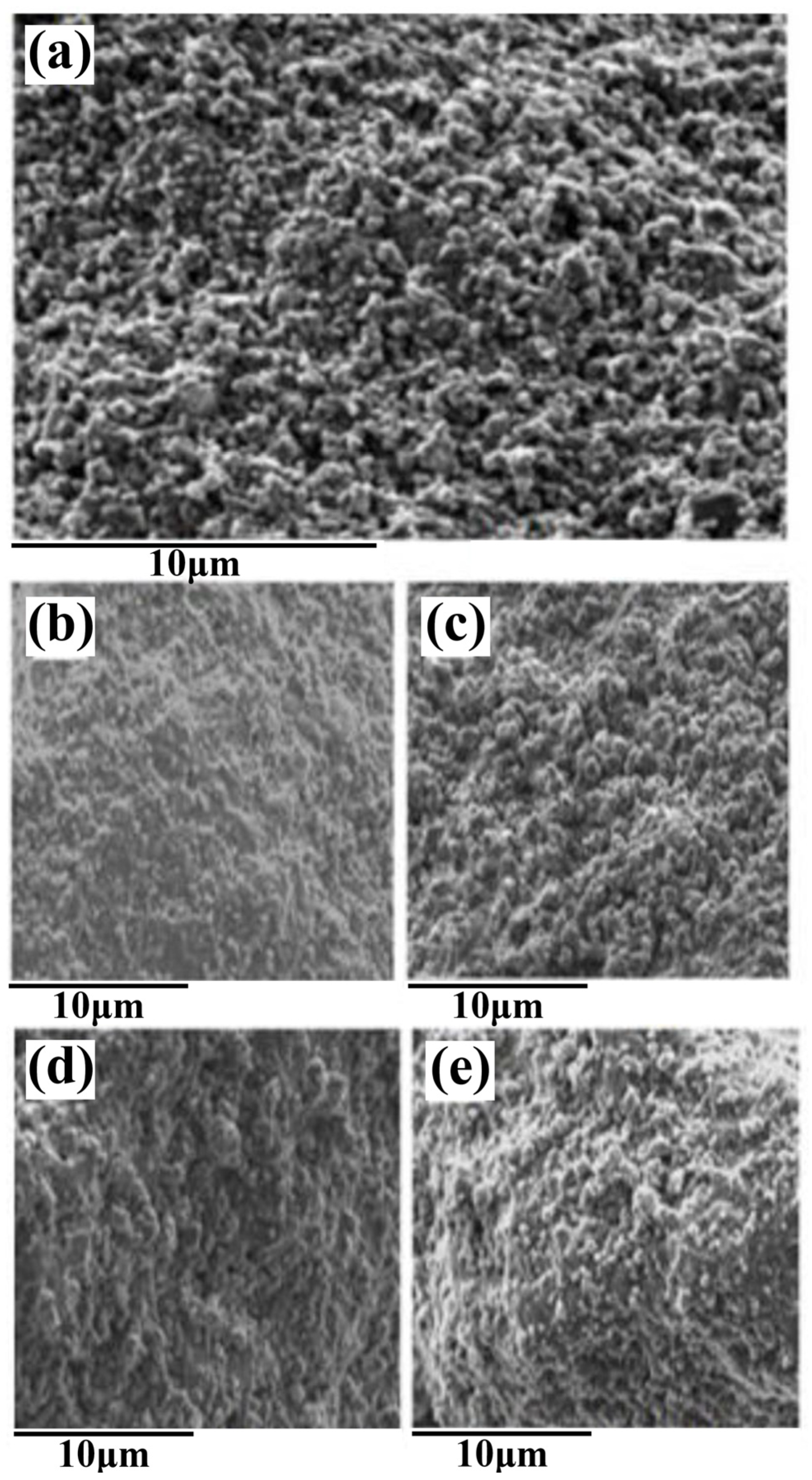
The SEM micrographs shown in Figure 2 provide visual representation of a single-phase material, which is further confirmed by X-ray diffraction, reported later in this section. Even though the existence of minor phases cannot be ruled out from such microstructural analysis, the presence of isolated phases was not detected even at magnifications of 15,000×. The composition analysis conducted by EDS agreed to within ±10% of the nominal composition of the samples as presented in Table 1.
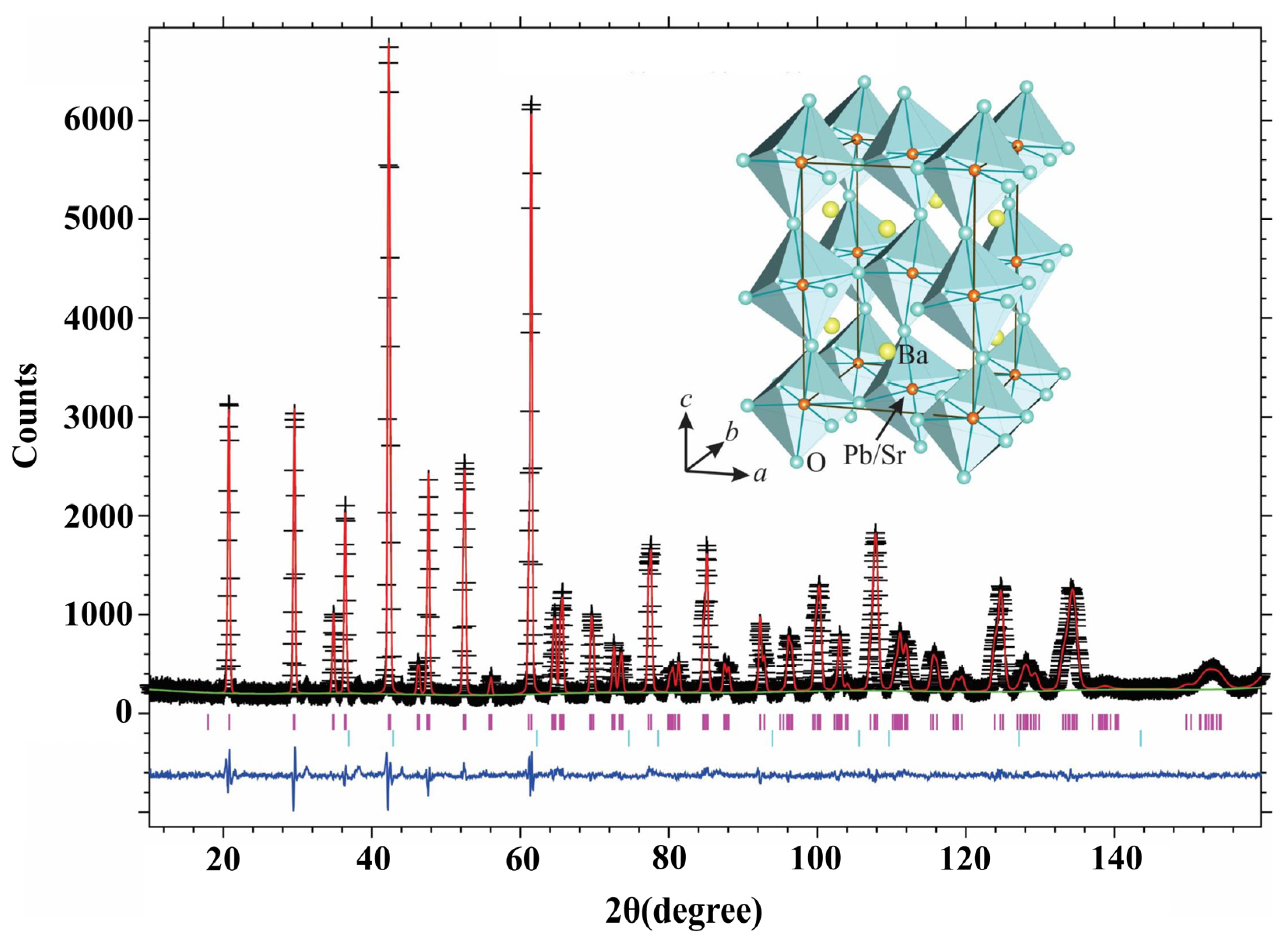
3.2. XRD
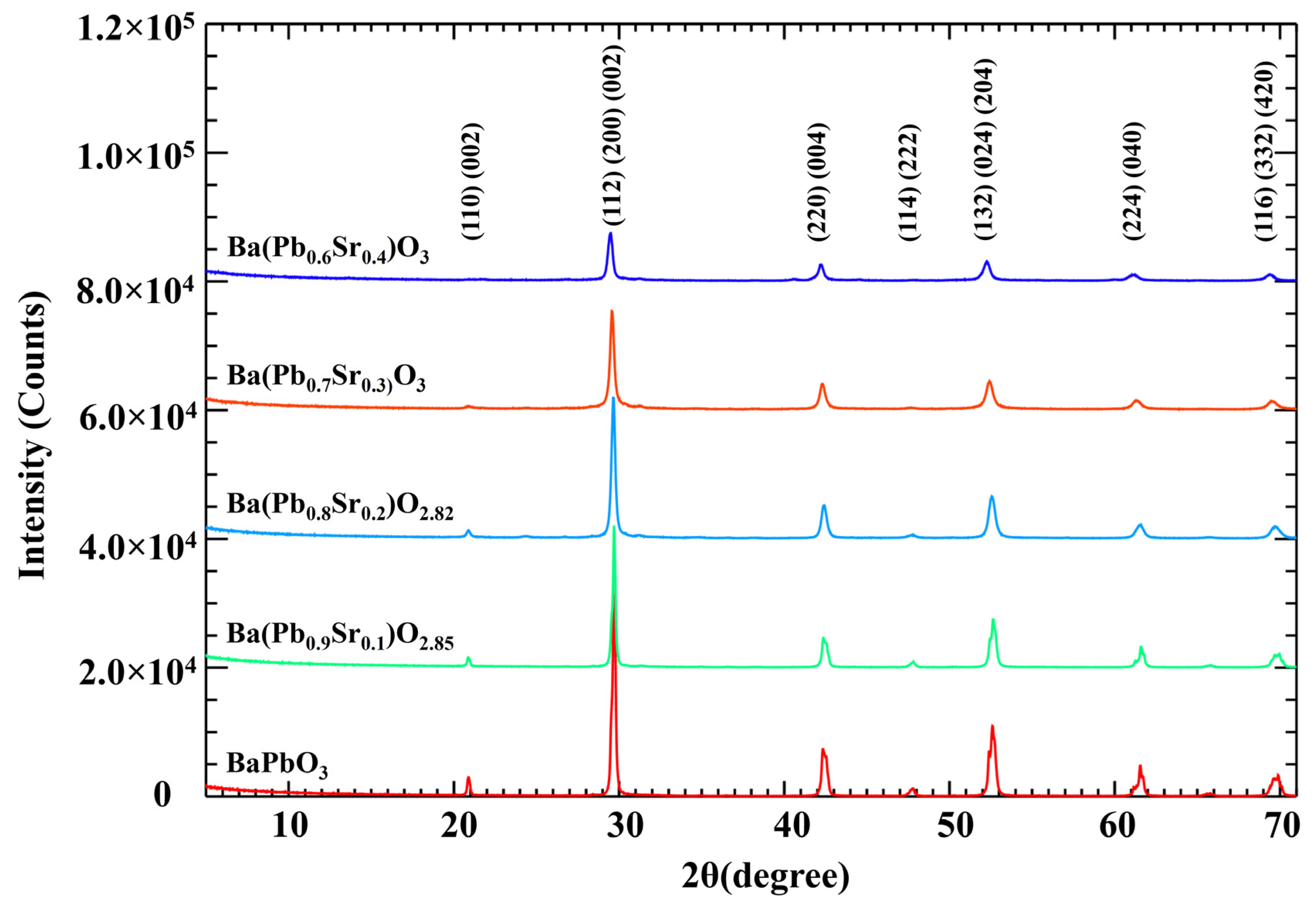
X-ray diffraction patterns of all the samples are presented in Figure 3. The diffraction pattern of pure BaPbO3 agrees with that reported earlier [7]. All samples of the Ba(Pb1−xSrx)O3−z series are black in color and are found to be chemically stable in atmospheric conditions. The XRD data presented in Figure 3 demonstrate that no appreciable precipitation of a second phase was detected up to 0.4 molar substitution of PbO2 by SrO. The characteristic XRD peaks of all the compositions (x = 0–0.4) have been indexed and compared with a similar system reported by Kodenkandath [7]. A distinguishable shift in the characteristic peaks was observed in some of the characteristic peaks with the substitution of PbO2 by SrO. The substitution of Pb4+ (0.775 Å) by Sr2+ (1.18 Å) is expected to increase the interplanar spacing, resulting in shifting of the reflections to smaller 2θ values. Such shifts are indicative of the dilation of the lattice parameters (interplanar spacing) rather than precipitation of a second phase.
3.3. Neutron Powder Diffraction
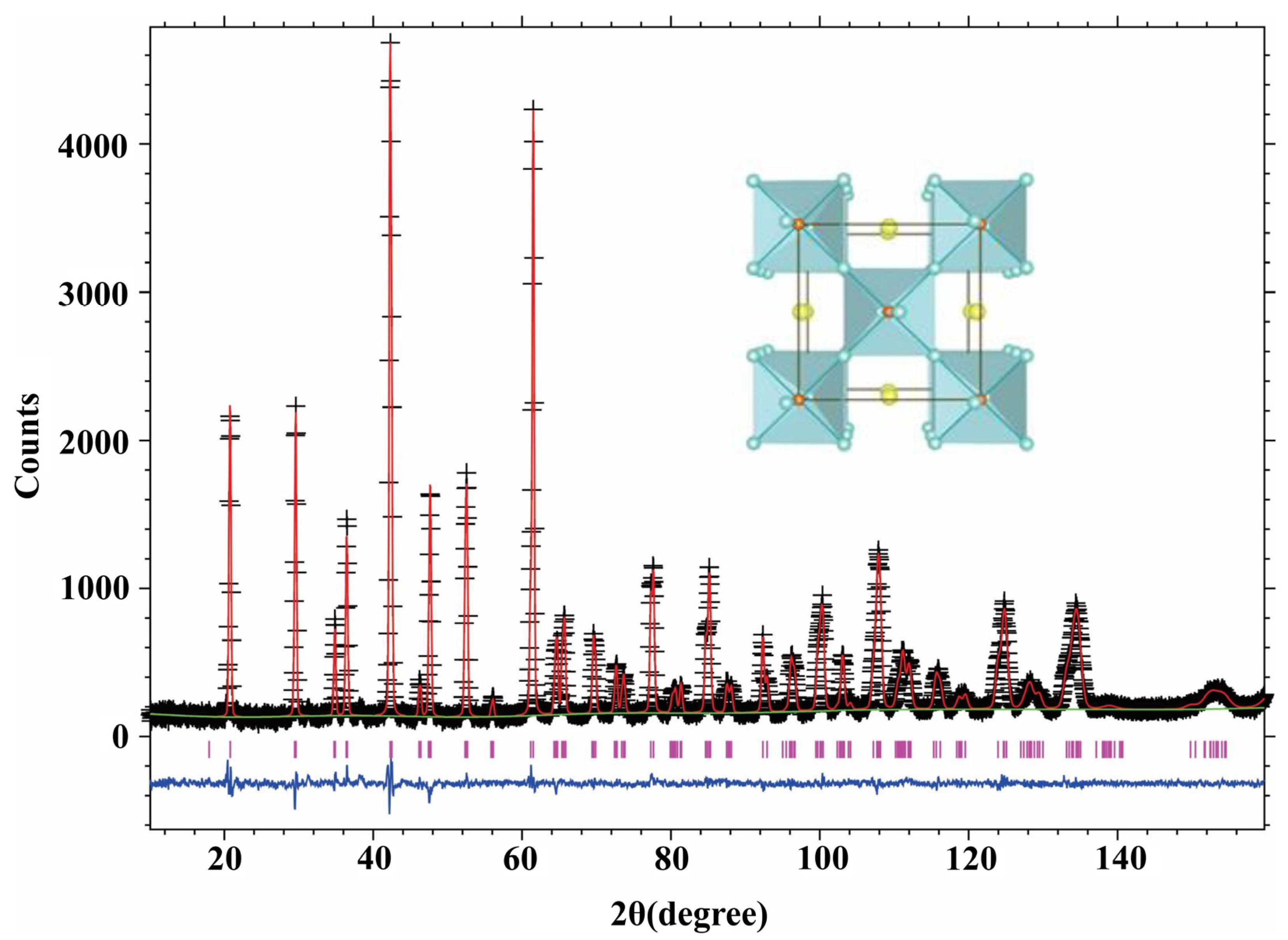
To demonstrate the oxygen deficient nature of the Sr-substituted compounds, two such compositions were randomly selected and the data are presented in Table 2 and Table 3 and Figure 4 and Figure 5. Refinements indicate that while the A site (4e site, Table 2 and Table 3) is fully occupied by Ba atoms, the Pb and Sr atoms are randomly distributed at the B sites (4a site, Table 2 and Table 3). This feature proves that the intended replacement of Pb+4 by Sr2+ has been successful. NPD analyses confirmed the oxygen deficient nature of the samples where Pb+4 ions were partially substituted by Sr2+ ions, whereas Yasukawa [1] found that the lattice parameters decreased when Sr2+ replaced Ba2+ on the latter’s site, our data shows that the lattice parameters increase as described earlier.
As described in the earlier section on XRD analysis, the orthorhombic to pseudo-cubic transformation observed earlier [4] was on account of Pb4+ ions being partially substituted by Cu2+ in the Ba(Pb1−xCux)O3−z system. As the radius ratio of Sr2+ (1.18 Å) to Pb4+ (0.775 Å) ions is 1.52, partial substitution of Pb4+ by Sr2+ is expected to introduce severe strain in the oxygen tetrahedra of the perovskite structure. Despite the introduction of considerable strain in the lattice, NPD data detected only a small amount (<1%) of second phase. The emergence of such minor phases is not expected to affect the conductivity of the samples significantly. Moreover, NPD studies indicate that despite the merger of the (004, 220) and (040, 224) reflections, even the distorted orthorhombic structure (for the x = 0.2 sample) of the perovskite has not undergone a transformation to a different crystal system.
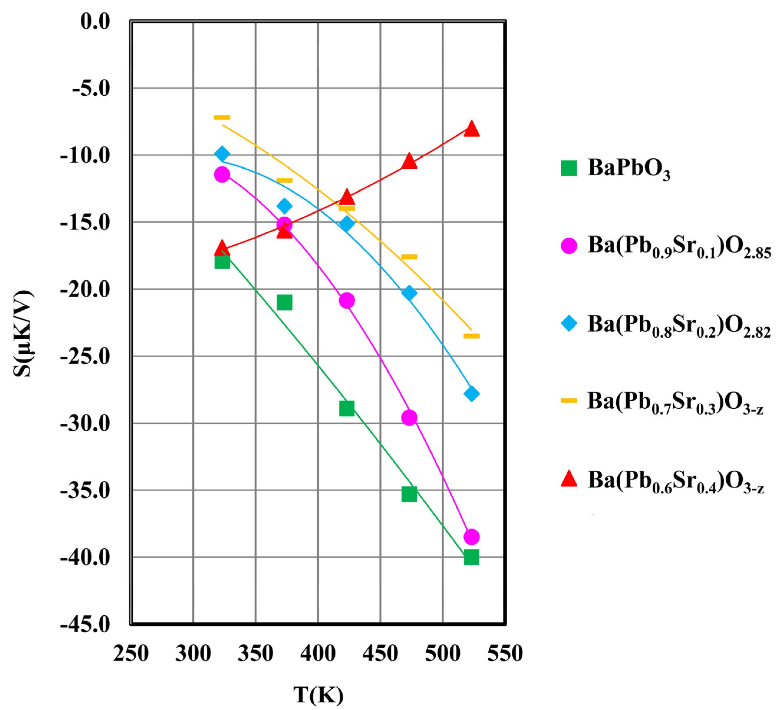
3.4. Thermopower
Thermopower (S) data of all the samples as a function of temperature are presented in Figure 6 and Table 1. S is observed to be negative for all samples but the absolute value decreases as x increases from 0 to 0.4 in the general composition of Ba(Pb1−xSrx)O3−z. The negative thermopower is consistent with electrons being the majority carriers of the starting compound, BaPbO3, which is also confirmed by its negative Hall coefficient reported elsewhere [9,16]. The reduction in electron concentration may also be understood from the simple chemical consideration that the introduction of SrO in place of PbO2 is a reduction phenomenon, which is observed in the oxygen deficient composition as determined by the analysis of neutron diffraction data presented in Figure 4 and Figure 5.
As described in an earlier section, substitution of Sr2+ for Pb4+ creates holes in the Ba(Pb1−xSrx)O3−z system of compounds. The concentration of carrier electrons is thus reduced by the introduction of Sr2+ ions, which are termed acceptors. Such reduction of the electron concentration reduces the absolute value of S as x increases from 0 to 0.4 (Figure 6 and Table 1).
A noticeable change in the behavior of thermopower as a function of temperature for the x = 0.4 sample is observed in Figure 6, whereas the absolute thermopower of all the samples in the composition range 0 ≤ x ≤ 0.3 increases with temperature, that of the x = 0.4 sample exhibits the opposite trend. Such variation of thermopower with temperature was also reported in the (Ba1−xSrx)PbO3 system by Yasukawa [9] who explained such behavior in terms of the reduced concentration of electrons at the Fermi level caused by the increased addition of Sr ions. We shall explain the origin of the anomalous variation of thermopower with temperature in a later section following the demonstration of a quantum phase transition taking place in a small composition range (0.1 ≤ x ≤ 0.2) of the Ba(Pb1−xSrx)O3−z system.
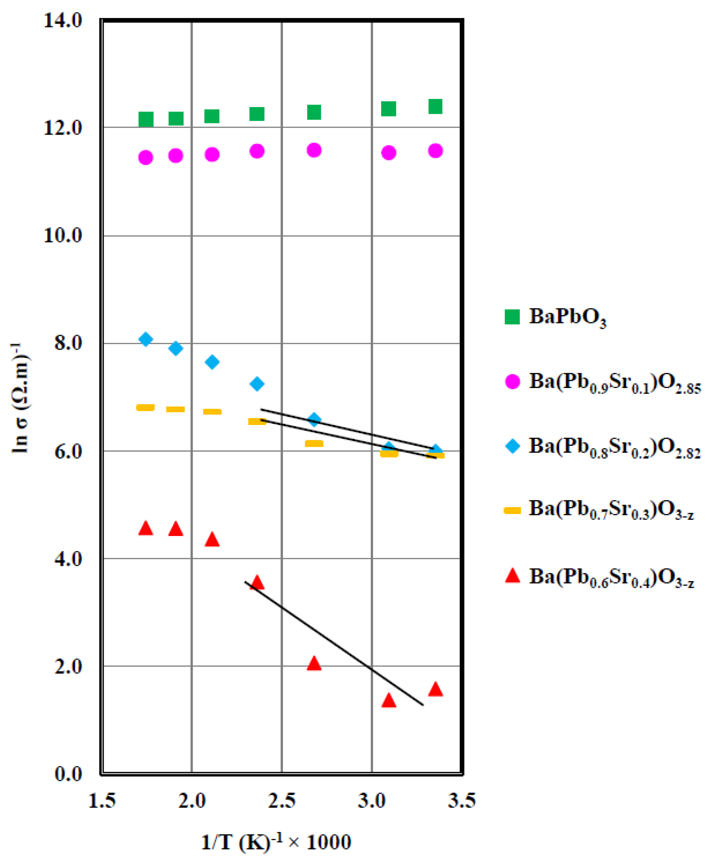
3.5. Electrical Conductivity
Figure 7 depicts the electrical conductivity (σ) of Ba(Pb1−xSrx)O3−z as a function of inverse temperature and composition. For the sample where x = 0, (i.e., pure BaPbO3) electrical conductivity decreases slightly with increasing temperature, which agrees with the results reported by Yasukawa et al. [9]. Such behavior is characteristic of a metal where conductivity is an unactivated process. Metallic conductivity typically decreases with increasing temperature on account of enhanced scattering of the charge carriers. Conductivity of an insulator or semiconductor, on the other hand, increases exponentially with temperature.
The temperature dependence of the x = 0.10 composition mimics that of pure BaPbO3 (x = 0), but exhibits lower conductivity as compared to the latter (Figure 7). The conductivity at 473K of all samples are listed in Table 1 to demonstrate the sharp decline in conductivity in the composition range 0 ≤ x ≤ 0.4. For the x = 0.2, 0.3, and 0.4 samples; however, σ not only decreases by several orders of magnitude as compared to BaPbO3 at all temperatures, but these compositions also exhibit semiconducting behavior in the sense that conductivity increases exponentially with temperature (T), following:
in the low temperature region, shown by trend lines in Figure 7. The activation energy, Ea, in Equation (1) is the activation energy for electrical conduction, which is approximately half of the optical band gap and K is the Boltzmann constant. The pre-exponential coefficient, σ0, is a constant that depends on several factors, including the overlap integral of adjacent carriers, the distance between them, their longitudinal optical frequencies, and the structure of the host lattice [10,14].
For an intrinsic semiconductor, a ln σ vs. 1/T plot should give a straight line as mandated by Equation (1). However, all the Sr-doped samples (Figure 7) deviate from such linearity as required by Equation (1) at higher temperatures. The nonlinearity of the ln σ vs. 1/T plot is explained as follows:
- (i)
- Carriers get increasingly trapped in the lattice, forming polarons, which are known to have considerably less mobility than bare/itinerant electrons. Such polarons favor formation at higher temperatures because of enhanced electron–phonon interaction.
- (ii)
- Sr-doping introduces holes to the valence band that may recombine with the electrons, thereby reducing electron/polaron (carrier) concentration. Reduced carrier concentration also leads to inevitable reduction in conductivity.
The activation energies, calculated using Equation (1) from the ln σ vs. 1/T plots of the x = 0.2, 0.3, and 0.4 samples, are listed in Table 1. For reasons outlined above, we have considered only the low temperature data for calculating the optical band gaps because polarons are relatively less likely to form in this temperature region. It is important to note that the band gap, deduced from the activation energies for the x = 0.2, 0.3, and 0.4 samples, will only be used to qualitatively suggest that the optical band gap of the samples increases with increasing x. Determination of the actual band gaps was not intended in this investigation.
From the analysis of the activation energy for electrical conduction, it is evident that the Ba(Pb1−xSrx)O3−z system exhibits metallic characteristics (Ea = 0) in the composition range 0 < x < 0.1. An optical band gap of 0.191 eV opens up at x = 0.2, which marks the transition to an insulating state. The band gap increases with increasing x, reaching a value of 0.48 eV for the x = 0.4 sample (Table 1). As will be shown in the next section, the transition from a metallic (x = 0, 0.1) to an insulating or semiconducting state at a composition of Ba(Pb0.8Sr0.2)O2.82 bears the feature of a Mott–Hubbard type MIT [17,18,19,20,26].
3.5.1. MIT in Ba(Pb1−xSrx)O3−z
The Hall coefficient measurement by Ikushima et al. [16] has established that the concentration of electrons at the Fermi level in BaPbO3 is ~2 × 10²⁰/cm3. The progressive and significant decrease in electrical conductivity as x increases from 0 to 0.4 in the general composition Ba(Pb1−xSrx)O3−z may be explained as follows: when Sr2+ ions replace Pb4+ ions in Ba(Pb1−xSrx)O3−z, the introduction of holes leads to a reduction in the electron concentration at the Fermi level. As a result, the effective overlap of the Pb-6s/O-2p orbitals is reduced, leading to a narrower sp-antibonding band [5,7,15]. Such a narrowing of the electron band leads to an increase in the Hubbard band gap (described in the next section) [19], which, in turn, leads to decreased conductivity. As stated earlier, substitution of Pb4+ by Sr2+ ions in BaPbO3 was targeted to drive the metallic properties of BaPbO3 towards a quantum phase transition by creating either oxygen vacancies and/or allowing partial reduction of Pb4+ to the unusual < 4+ valence for Pb in the lattice [7,15].
The changes observed in the ln σ vs. 1/T plots for different compositions presented in Figure 7 and Table 1 have demonstrated that a metal to insulator transition has been observed for Ba(Pb1−xSrx)O3−z at a critical Sr2+ ion composition of x = 0.2. A concomitant increase in the optical band gap from 0.192 to 0.480 eV as x increases from 0.2 to 0.4 is observed, as described earlier. We explain the transition from metallic to semiconducting behavior in the composition range 0.1 ≤ x ≤ 0.2 in terms of a Mott–Hubbard transition [17,18,19,20] by taking into account the intra-atomic interaction of a pair of electrons at a site in the crystal lattice. A Mott–Hubbard type MIT is a quantum phase transition signifying the transformation of an insulator to a metallic conductor (or vice versa) when the density of electrons increases as a result of compositional changes or on account of temperature/pressure variations. In the following, two basic models of MIT pertinent to the present investigation are described briefly.
Hubbard Model of MIT
In crystalline materials, the Hubbard model [19] assumes the tight-binding approximation where electrons are envisaged to “hop” between the orbitals of atoms. Such hopping takes place within a hopping or transfer integral, giving rise to electron bands. The amplitude of overlapping orbitals determines the width of such bands. Canonical band theory does not consider electron–electron interactions. The Hubbard model takes into account the Coulomb repulsion encountered by electrons when they are located on the same atomic orbital. The Hamiltonian that Hubbard proposed contains a term that accounts for the energy, U, for such pairs of electrons, which is given by [18,19]:
Here, κ is the dielectric constant of the medium, the wave functions of the two electrons on a site are represented by ψ (x1), ψ (x2), and r12 is the distance between the electrons. The competition between the hopping integral and Coulomb repulsion between carriers on the same site are evident in the Hubbard model.
The Hubbard model can be used to explain the transition from metallic to insulating behavior in certain oxides by the increase in carrier spacing, which effectively reduces the “hopping integral”, which enhances the effect of the on-site potential. Such an increase in the nearest-neighbor spacing can best be achieved by reducing the concentration of the charge carriers. In the case of Ba(Pb1−xSrx)O3−z, substitution of Pb4+ by Sr2+ ions serves the purpose of reducing the concentration of carrier electrons by creating holes that readily recombine with the electrons at the Fermi level. Such variations of the hopping integral have been used to explain the transition from metal to insulator in a large number of systems [17,18,19,26]. Such a transition from a metal to an insulator occurs when the on-site repulsion completely negates the effect of the hopping integral as described in the following.
If an electron is removed from a center by the aliovalent cation substitution (e.g., Sr2+ replacing Pb4+) of a compound, a hole is created in a band of width B1, which may be termed the ‘lower Hubbard band’. Likewise, an electron placed on a site already occupied, produces a band of width B2, termed the ‘upper Hubbard band’, is higher in energy than the lower Hubbard band. The concept of the formation of two such Hubbard bands has been effectively used by Mott [17,18] to explain MIT, where the ‘Hubbard U’ was defined as the separation between the centers of the two bands and it was demonstrated that such a system would exhibit insulating behavior if:
If, however, the electron (donor) concentration is increased, the widths of the two bands (B1 and B2) would increase, too. At a critical concentration of donors, the bands would overlap and exhibit an insulator to metallic transition. A discontinuous (or abrupt) transition is expected when:
Mott Model of MIT
A simpler model for describing the metal–insulator transition was formulated by Mott [17,18,20], which also took into account the “on site” electron–electron (Coulomb repulsion) interaction in solids. In the “tight-binding approximation” and considering no interaction among electrons, the single electrons donated by the dopants would always form a half-filled band and hence always exhibit metallic conduction. However, in a doped semiconductor, the activation energy for conduction is finite and the conductivity decreases with decreasing temperature, eventually reaching zero at 0 K. Similarly, as the dopant concentration is increased, the activation energy for conduction decreases and eventually vanishes to give metallic conduction. Such a conversion of non-metallic (semiconducting or insulating) to metallic behavior is known as a Mott transition. In other words, the Mott model considers the behavior of an electron as a function of the density and interaction among valence electrons.
The key to Mott transitions is the repulsion between two carriers on the same site, which is the same as the ‘Hubbard U’, as described earlier. Mott showed that there is a critical density of electrons, Nc, above which the charge carriers (e.g., valence electrons or holes) are no longer bound by their individual nuclei. Instead, they become itinerant. Viewed from the semiconducting or insulating state, this critical density marks the transition to the metallic state, and is given by the Mott criterion:
In Equation (5), Nc is the carrier concentration and aH is an effective “Bohr” radius for the carriers (electrons or holes) in the low-density limit, where semiconducting behavior or electron localization ensues.
It has been established that localized carriers in semiconductors almost always deform the surrounding lattice [18,20]. The pseudoparticle comprising the carrier and the associated lattice deformation is known as a polaron and such electron–phonon interaction increases with temperature. The effective Bohr radius of a carrier on the low-density (insulating) side of a Mott transition is actually the radius of such polarons, rp, which can be calculated using the following equation [20,21]:
The most important feature of the Mott criterion is Nc, the critical concentration of valence electrons at which the transition of metal to insulator takes place and is consistent with the Hubbard model [19]. However, the Mott criterion for MIT is independent of crystallinity or the periodic structure of atoms in a solid and hence is considered universal. The Mott criterion has been found to be applicable to diverse systems such as metallic solutions in liquid ammonia and also in doped semiconductors.
The substitution of a Pb4+ by a Sr2+ ion removes two electrons from a nearby Pb-6s/O-2p band by the creation of holes as described earlier. Such electron removal from one center to another is the same as the concept of two “Hubbard bands” [17,18,20], where an electron is considered to have been moved from one center to another. The hole has a certain wavenumber, giving rise to a band of width B1. On the other hand, an electron placed on a site that is occupied can also move in a band of width, say, B2. The separation between the centers of the B1 and B2 bands is the Hubbard U, described earlier in Equations (2)–(4). The condition shown in Equation (4): U = ½ (B1 + B2) appears to be satisfied in the composition range 0.1 < x ≤ 0.2, where the metal to semiconductor transition is observed as depicted in Figure 7.
In support of this observation, we reproduce the Edwards/Sienko (ES) plot [26] in Figure 8, which depicts MIT in a diverse category of materials. ES plot is a compilation of experimental data obtained from a multitude of sources and reproduced on a log–log scale. Edwards and Sienko attributed the universality of the Mott criterion to its adherence to the Hubbard model.
A linear relationship has been shown to exist between the effective radii of the carriers, rp, and the critical concentration, Nc, of the Mott criterion in a large number of materials. The relationship, Nc⅓. aH ~ 0.26, is applicable over a range of approximately1010 in critical carrier densities (Nc) and also a large range in Bohr radii (aH). Edwards and Sienko [26] defined aH as an appropriate radius associated with a realistic wave function for the localized state in the insulating side of the transition, which we have defined by the polaron radius, rp, in this investigation. It is important to note that the Mott constant (RHS of Equation (5)), varies in a range of 0.2–0.4 for different compounds, as is evident from the ES plot.
Even though the MIT in the Ba(Pb1−xSrx)O3−z system takes place in a narrow range of composition, viz., 0.1 < x ≤ 0.2. (Figure 7), we base our calculations on the x = 0.2 sample. The choice of the x = 0.2 sample to test the Mott criterion is considered appropriate for the following reasons: (i) the concentration of charge carriers is always taken on the insulating side of the Mott transition [17,18,19,20,26], and (ii) as both axes of the ES plot are in logarithmic scale, a small change in composition would not appreciably alter the position of the sample on this plot. For the x = 0.2 sample, 20% of the Pb ions has been replaced by Sr ions. Hence, the electron concentration (Nc) for the Ba(Pb0.8Sr0.2)O2.82 sample is considered to be approximately 80% of the carrier concentration of BaPbO3 because the concentration of electrons in the Pb-6s/O-2p hybrid orbitals is reduced by the Sr2+ ions. As the carrier concentration of undoped BaPbO3, determined by Ikushima and Hayakawa [13], is 2 × 10²⁰/cm3, the electron concentration of the x = 0.2 sample is estimated at 1.6 × 10²⁰/cm3. Using this value of Nc in Equation (5), the effective radius of the electrons of the x = 0.2 sample is determined to be 7.4 × 10⁻⁸ cm (Mott constant ~0.39), which falls right along the straight line of the ES plot, as shown by the asterisk in Figure 8, demonstrating a Mott–Hubbard type metal–insulator transition in the Ba(Pb1−xSrx)O3−z system.
The evolution of the electronic structure of the Ba(Pb1−xSrx)O3−z series may also be understood starting with the x = 0.4 sample, as the carrier concentration is increased by decreasing x (Sr content). This sample has the characteristics of an insulator where conductivity increases exponentially with temperature (Figure 7). Moreover, the activation energy for dc conduction is observed to decrease and conductivity increases as x is reduced until it reaches the metallic state at x = 0.1, where the activation energy vanishes and the sample turns metallic (Table 1). At x = 0, (undoped BaPbO3) the conductivity is highest among all the samples because it has the highest carrier concentration. It also exhibits unactivated conduction (zero activation energy), typical of a metal.
As the activation energy for conduction is approximately equal to half of the optical band gap of the insulating samples, decreasing x, (increasing carrier concentration) results in decreasing the Hubbard U (Equations (3) and (4)). As the sample with x = 0.4 has the lowest carrier concentration, the U is expected to be largest among all samples in the Ba(Pb1−xSrx)O3−z system and, predictably, it exhibits the lowest conductivity (Figure 7). As x is decreased from 0.4, the concentration of carriers increases with a concomitant increase in the bandwidths of B1 and B2 until it reaches the composition x = 0.1 where the B1 and B2 bands overlap and the material undergoes a quantum phase transition to a metallic state.
The Mott–Hubbard type phase transition described above can be used to explain the anomaly observed in the thermopower vs. temperature behavior of the x = 0.4 sample of the Ba(Pb1−xSrx)O3−z system (Figure 6). Samples x = 0 and 0.1 are metallic as evidenced by their unactivated conduction. The lower thermopower exhibited by the x = 0.1 sample as compared to the undoped BaPbO3 is attributed to the reduced electronic concentration on account of the holes introduced in the system when Pb4+ is substituted by Sr2+ ions.
As discussed above, a quantum phase transition to an insulating state takes place in the narrow composition range 0.1 < x ≤ 0.2. The x = 0.2 and x = 0.3 samples fall on the insulating side of the quantum transition, the band gaps of which are relatively narrow (~ 0.2 eV, Table 1) and the dopant level lower than those of the x = 0.4 sample (band gap ~ 0.5 eV, Table 1). The concentration of electrons in the conduction band (CB), which are responsible for the negative thermopower, varies exponentially on the band gap. Consequently, the x = 0.2 and x = 0.3 samples have sizeable concentrations of free electrons in the CB, which would increase exponentially with temperature. The holes contributed by the lower Sr-doping levels in the x = 0.2 and x = 0.3 compositions are overwhelmed by the abundance of free electrons in the CB, causing the negative thermopower to increase monotonously with temperature.
For the x = 0.4 sample, the concentration of electrons in the CB is expected to be significantly lower than those of the x = 0.2 and x = 0.3 samples. Moreover, the larger hole concentration of the x = 0.4 sample contributes a significant positive thermopower, resulting in the anomalous thermopower vs. temperature trend observed in Figure 6.
4. Conclusions
A metal to insulator transition (MIT) has been observed in a narrow range of composition (0.1 < x ≤ 0.2) in the Ba(Pb1−xSrx)O3−z system. Despite the fact that the radius of Sr2+ ions is more than 50% larger than that of the Pb4+ions that they substitute, a second phase has not been detected by XRD, neutron diffraction measurements, or scanning electron microscopy up to x = 0.4. The Sr2+ ions, which substitute the Pb4+ ions, reduce the electron concentration of the base material, BaPbO3, by acting as acceptors in the host lattice. At x = 0.2, the Ba(Pb1−xSrx)O3−z system exhibits a quantum phase transition from a metal to an insulator phase, which has been demonstrated to be a Mott–Hubbard type quantum transition.
Author Contributions
Conceptualization, A.M.E. and B.D.; methodology, A.M.E., B.D., A.K., W.W.-N. and Q.H.; software, A.M.E., I.P. and A.K.; validation, A.M.E., B.D., I.P.; formal analysis, A.M.E. and B.D.; investigation, A.M.E. and B.D.; resources, I.P., W.W.-N. and Q.H.; data curation, A.M.E.; writing—original draft preparation, A.M.E.; writing—review and editing, B.D. and A.K.; visualization, A.M.E. and B.D.; supervision, B.D.; project administration, B.D.; funding acquisition, I.P. All authors have read and agreed to the published version of the manuscript.
Funding
This research received internal funding from Vitreous State Laboratory, The Catholic University of America.
Institutional Review Board Statement
Not applicable.
Informed Consent Statement
Not applicable.
Data Availability Statement
The data presented in this study are available on request from the corresponding author.
Acknowledgments
The authors would like to acknowledge the contribution of the National Institute of Standard and Technology, Gaithersburg, MD, USA, for allowing us to utilize their facilities for the Neutron Powder Diffraction facilities. The contribution of Vitreous State Laboratory of the Catholic University of America, Washington, DC, USA, is also acknowledged for allowing the authors to utilize all other equipment for the experiments performed in the course of this investigation.
Conflicts of Interest
The authors declare no conflict of interest. The funders had no role in the design of the study; in the collection, analyses, or interpretation of data; in the writing of the manuscript, or in the decision to publish the results.
References
- Yasukawa, M.; Murayama, N. High-temperature thermoelectric properties of the oxide material: Ba1−xSrxPbO3 (x = 0–0.6). J. Mater. Sci. Lett. 1997, 16, 1731–1734. [Google Scholar] [CrossRef]
- Zhang, J.; Hu, B.; Xu, J.; Gu, Z.; Zhang, S. Phase, microstructure and conductivity of electron-doped Ba1−xLaxPbO3 ceramics. Ceram. Int. 2014, 40, 10825–10830. [Google Scholar] [CrossRef]
- Fu, W.T.; Ijdo, D.J.W.; Visser, D. High-resolution neutron powder diffraction study on the structure of BaPbO3. Solid State Commun. 2005, 134, 647–652. [Google Scholar] [CrossRef]
- Roth, R.S. Classification of Perovskite and Other ABO3-Type Compounds. J. Res. Natl. Bur. Stand. 1957, 58, 75–78. [Google Scholar] [CrossRef]
- Xin, W.; Yudong, L.; Zhiqiang, Z. Defect Compensating Mechanism Undoped Barium Plumbate. J. Chin. Ceram. Soc. 2007, 35, 701–704. [Google Scholar]
- Fu, W.T.; Ijdo, D.J.W. A Comparative Study on the structure of APbO3 (A = Ba,Sr). Solid State Commun. 1995, 95, 581–585. [Google Scholar] [CrossRef]
- Kodenkandath, T. Structure and properties of substituted BaPbO3 and Ba2PbO4 compounds. Mater. Chem. Phys. 2000, 62, 23–28. [Google Scholar] [CrossRef]
- Menushenkov, A.P.; Klementev, K.V. Extended x-ray absorption fine-structure indication of a double-well potential for oxygen vibration in Ba1−xKxBiO3. J. Phys. Condens. Matter 2000, 12, 3767–3786. [Google Scholar] [CrossRef]
- Yasukawa, M.; Murayama, N. A promising oxide material for high-temperature thermoelectric energy conversion: Ba1−xSrxPbO3 solid solution system. Mater. Sci. Eng. 1998, B54, 64–69. [Google Scholar] [CrossRef]
- Cava, R.J.; Batlogg, B.; Espinosa, G.P.; Ramirez, A.P.; Krajewski, J.J.; Peck, W.F.; Rupp, L.W., Jr.; Cooper, A.S. Superconductivity at 3.5 K in BaPb0.75Sb0.25O3: Why is Tc so low? Nature 1989, 339, 291–293. [Google Scholar] [CrossRef]
- Sleight, A.W.; Gillson, J.L.; Bierstedt, P.E. High-Temperature Superconductivity in The BaPb1−xBixO3 System. Solid State Commun. 1975, 17, 27–28. [Google Scholar] [CrossRef]
- Wignacourt, J.P.; Swinnea, J.S.; Steinfink, H.; Goodenough, J.B. Oxygen atom thermal vibration anisotropy in Ba0.87K0.13BiO3. Appl. Phys. Lett. 1988, 53, 1753–1755. [Google Scholar] [CrossRef]
- Itoh, M.; Sawada, T.; Kim, I.S.; Inaguma, Y.; Nakamura, T. Composition Dependence of Carrier Concentration and Conductivity in (Ba1−xSrx)PbO3-δ. Solid State Commun. 1992, 83, 33–36. [Google Scholar] [CrossRef]
- Kharton, V.V.; Viskup, A.P.; Kovalevsky, A.V.; Naumovich, E.N.; Marques, F.M.B. Ionic transport in oxygen-hyperstoichiometric phases with K2NiF4-type structure. Solid State Ion. 2001, 143, 337–353. [Google Scholar] [CrossRef]
- Mattheiss, L.F. Electronic structure of the Ban+1PbnO3n+1 homologous series. Phys. Rev. B 1990, B42, 359–365. [Google Scholar] [CrossRef]
- Ikushima, H.; Hayakawa, S. Electrical Properties of BaPbO3 Ceramics. Solid State Electron. 1996, 9, 921–925. [Google Scholar] [CrossRef]
- Edwards, P.P.; Johnston, R.L.; Rao, C.N.R.; Tunstall, D.P.; Hensel, F. The metal-insulator transition: A perspective. Philos. Trans. R. Soc. Lond. 1998, 356, 5–22. [Google Scholar] [CrossRef]
- Mott, N.F. The transition to the Metallic State. Philos. Mag. Lett. 1961, 6, 287–309. [Google Scholar] [CrossRef]
- Hubbard, J. Electron Correlations in Narrow Energy Bands. Proc. R. Soc. Lond. 1963, 276, 238–257. [Google Scholar]
- Mott, N. Conduction in Non-Crystalline Materials, 2nd ed.; Oxford Science Publications: Oxford, UK, 1993. [Google Scholar]
- Greaves, G.N. Small Polaron Conduction in V2O5-P2O5 Glasses. J. Non-Cryst. Solids 1973, 11, 427–446. [Google Scholar] [CrossRef]
- Toby, B.H. EXPGUI, A graphical user interface for GSAS. J. Appl. Cryst. 2001, 34, 210–213. [Google Scholar] [CrossRef] [Green Version]
- Larson, A.C.; Von Dreele, R.B. General Structure Analysis System (GSAS); Los Alamos National Laboratory Report LAUR: Los Alamos, NM, USA, 2000; pp. 86–748. [Google Scholar]
- Bhatta, R.P.; Annamalai, S.; Mohr, R.K.; Brandys, M.; Pegg, I.L.; Dutta, B. High temperature thermal conductivity of platinum microwire by 3ω method. Rev. Sci. Instrum. 2010, 81, 114904. [Google Scholar] [CrossRef] [PubMed]
- Eufrasio, A. Electrical and Thermal Transport in Cation Substituted Barium Plumbate. Ph.D. Thesis, The Catholic University of America, Washington, DC, USA, 2019. [Google Scholar]
- Edwards, P.P.; Sienko, M.J. Universality aspects of the metal-nonmetal transition in condensed media. Phys. Rev. 1978, B17, 2575–2581. [Google Scholar] [CrossRef]
Figure 1.
(a) Cubic perovskite structure of BaPbO3. (b) Oxygen octahedra centered around Pb4+ ions, also showing distribution of the oxygen tetrahedra surrounding Ba2+ ions. (c) Coordination of O2− ions around and Ba2+ ions.
Figure 1.
(a) Cubic perovskite structure of BaPbO3. (b) Oxygen octahedra centered around Pb4+ ions, also showing distribution of the oxygen tetrahedra surrounding Ba2+ ions. (c) Coordination of O2− ions around and Ba2+ ions.

Figure 2.
Scanning electron micrograph of: (a) BaPbO3, (b) Ba(Pb0.9Sr0.1)O2.85, (c) Ba(Pb0.8Sr0.2)O2.82, (d) Ba(Pb0.7Sr0.3)O3, and (e) Ba(Pb0.6Sr0.4)O3.
Figure 2.
Scanning electron micrograph of: (a) BaPbO3, (b) Ba(Pb0.9Sr0.1)O2.85, (c) Ba(Pb0.8Sr0.2)O2.82, (d) Ba(Pb0.7Sr0.3)O3, and (e) Ba(Pb0.6Sr0.4)O3.

Figure 3.
X-ray diffraction patterns of Ba(Pb1−xSrx)O3−z for x = 0.0, 0.1, 0.2, 0.3, and 0.4.

Figure 4.
Neutron powder diffraction (NPD) data for BaPb0.9Sr0.1O2.85.

Figure 5.
Neutron powder diffraction (NPD) data for BaPb0.8Sr0.2O2.82.

Figure 6.
Thermopower vs. temperature of Ba(Pb1−xSrx)O3−z for x = 0.0, 0.1, 0.2, 0.3, and 0.4.

Figure 7.
Electrical conductivity vs. inverse temperature of Ba(Pb1−xSrx)O3−z for x = 0.0, 0.1, 0.2, 0.3, and 0.4. Trend lines in the low temperature region qualitatively demonstrates increasing band gap with increasing Sr doping.
Figure 7.
Electrical conductivity vs. inverse temperature of Ba(Pb1−xSrx)O3−z for x = 0.0, 0.1, 0.2, 0.3, and 0.4. Trend lines in the low temperature region qualitatively demonstrates increasing band gap with increasing Sr doping.

Figure 8.
The Edwards–Sienko plot represents a large number of diverse systems exhibiting MIT. The Ba(Pb0.8Sr0.2)O2.82 sample of the present investigation is represented by an asterisk. MIT is observed in the Ba(Pb1−xSrx)O3−z series when x < 0.2.
Figure 8.
The Edwards–Sienko plot represents a large number of diverse systems exhibiting MIT. The Ba(Pb0.8Sr0.2)O2.82 sample of the present investigation is represented by an asterisk. MIT is observed in the Ba(Pb1−xSrx)O3−z series when x < 0.2.


Table 1.
Composition, density, and transport data of Ba(Pb1−xSrx)O3−z.
| Composition | Activation Energy, Eg(eV) * | Optical Band Gap (eV) | Density (g/cm3) | Ln(σ) (Ω.m)−1 at 473 K | Thermopower (μV/K) at 473 K |
|---|---|---|---|---|---|
| BaPbO3−z | - | - | 6.23 | 12.21 | −35.3 |
| Ba(Pb0.9Sr0.1)O2.85 | - | - | 6.22 | 11.50 | −29.6 |
| Ba(Pb0.8Sr0.2)O2.82 | 0.096 | 0.191 | 5.86 | 7.65 | −20.3 |
| Ba(Pb0.7Sr0.3)O3−z | 0.101 | 0.202 | 5.68 | 6.72 | −17.6 |
| Ba(Pb0.6Sr0.4)O3−z | 0.240 | 0.480 | 5.50 | 4.36 | −10.4 |
* Calculated from low temperature region of the ln σ vs. 1/T plot.
Table 2.
Refined structure parameters for BaPb0.9Sr0.1O2.85 at room temperature.
| Atom | Site | x | y | z | n | B11 (Å2) | B22 (Å2) | B33 (Å2) | B12 (Å2) | B13 (Å2) | B23 (Å2) |
|---|---|---|---|---|---|---|---|---|---|---|---|
| Ba | 4e | 0.5001 (7) | 0 | ¼ | 1 | 1.09 (6) | 1.1 (1) | 0.068 (9) | 0 | 0 | 0 |
| Pb/Sr | 4a | 0 | 0 | 0 | 0.9/0.1 | 0.71 (5) | 0.92 (6) | 0.3 (1) | 0 | −0.10 (6) | - |
| O(1) | 4e | 0.0515 (5) | 0 | ¼ | 0.94 (1) | 1.6 (1) | 3.0 (2) | 0.3 (1) | 0 | 0 | 0 |
| O(2) | 8g | ¼ | ¼ | −0.0275 (2) | 0.956 (8) | 1.76 (8) | 1.8 (1) | 1.86 (8) | −0.86 (9) | 0 | 0 |
Rp(%) = 4.52, Rwp(%) = 5.84, χ2 = 1.03.
Table 3.
Refined structure parameters for BaPb0.8Sr0.2O2.82 at room temperature.
| Atom | Site | x | y | z | n | B11 (Å2) | B22 (Å2) | B33 (Å2) | B12 (Å2) | B13 (Å2) | B23 (Å2) |
|---|---|---|---|---|---|---|---|---|---|---|---|
| Ba | 4e | 0.5002 (6) | 0 | ¼ | 1 | 1.14 (7) | 1.1 (1) | 0.90 (9) | 0 | 0 | 0 |
| Pb/Sr | 4a | 0 | 0 | 0 | 0.79/0.21 (2) | 0.65 (5) | 0.80 (6) | 0.24 (6) | 0 | −0.10 (6) | - |
| O(1) | 4e | 0.0510 (5) | 0 | ¼ | 0.89 (1) | 1.4 (1) | 2.6 (2) | 0.2 (1) | 0 | 0 | 0 |
| O(2) | 8g | ¼ | ¼ | −0.0269 (2) | 0.963 (9) | 1.60 (8) | 2.1 (2) | 1.90 (9) | −0.91(6) | 0 | 0 |
Rp(%) = 4.61, Rwp(%) = 5.82, χ2 = 1.399.
Publisher’s Note: MDPI stays neutral with regard to jurisdictional claims in published maps and institutional affiliations. |
© 2021 by the authors. Licensee MDPI, Basel, Switzerland. This article is an open access article distributed under the terms and conditions of the Creative Commons Attribution (CC BY) license (https://creativecommons.org/licenses/by/4.0/).
Share and Cite
MDPI and ACS Style
Eufrasio, A.M.; Pegg, I.; Kafle, A.; Wong-Ng, W.; Huang, Q.; Dutta, B. Metal–Insulator Transition in Doped Barium Plumbates. Electron. Mater. 2021, 2, 428-444. https://doi.org/10.3390/electronicmat2030029
AMA Style
Eufrasio AM, Pegg I, Kafle A, Wong-Ng W, Huang Q, Dutta B. Metal–Insulator Transition in Doped Barium Plumbates. Electronic Materials. 2021; 2(3):428-444. https://doi.org/10.3390/electronicmat2030029
Chicago/Turabian StyleEufrasio, Andreza M., Ian Pegg, Amrit Kafle, Winnie Wong-Ng, Qingzhen Huang, and Biprodas Dutta. 2021. "Metal–Insulator Transition in Doped Barium Plumbates" Electronic Materials 2, no. 3: 428-444. https://doi.org/10.3390/electronicmat2030029