Receiver sensitivity and noise coupling to antenna are two major concerns when developing mobile devices such as smart phones and tablets. There are various causes of degradation of receiver sensitivity. However, most of the time they are due to the noise generated by digital signal harmonics on printed circuit board (PCB) patterns, which couple to the antennas. This article presents a methodology to predict noise to antenna coupling and antenna desense. The method is implemented by means of 3D EM simulation of the relative coupling level in a mobile device.
By assuming time-invariant linear media in the electromagnetic model, the reciprocity principle for the antenna systems holds. It implies that antennas work equally well as transmitters or receivers, and specifically that an antenna's radiation and receiving patterns are identical. Signals to antenna interference is therefore estimated by considering the magnetic (H) field maps and assuming the antenna as noise source.
Intra-system electromagnetic compatibility (EMC), or radio-frequency interference (RFI), is a challenging problem in modern electronics. Receiver sensitivity and noise coupling to antenna are two major issues when developing mobile devices such as smart phones and tablets. A mobile phone antenna and its receiver form an RF module that can detect signals as weak as -120dBm in a 200 KHz bandwidth, if not disturbed by nearby electronics. However, the clock frequencies of a smart phone can reach GSM880-1800 as well as Bluetooth and Wi-Fi bands (as illustrated in Figure 1a).The harmonics and data signals couple to the antenna and de-sensitize (desense) the RF system, thereby degrading the communication quality.
Desense represents the degradation in receiver sensitivity due to noise within the device. It limits the receiver’s ability to detect low-level signals, thus reducing the overall range and data rate. Figure 1b depicts the typical scenario of a communication system with receiver’s sensitivity affection from some in-device components.

Figure 1. a): frequency band for wireless communications in mobile devices and b): typical RFI and desense mechanism for a mobile phone system
There are various causes of degradation of receiver sensitivity. Most of the cases are due to the noise generated by digital signal harmonics on printed circuit board (PCB) patterns, which couple to the antennas. For instance, USB 3.0 [1], recently introduced in high-end smart phones, has very high data rate (5Gbps and 10Gbps for the variation 3.1 with a Nyquist frequency of 2.5 GHz and 5GHz respectively).
These high data rates involve clock and data signals with very fast transition times in the range of hundreds of picoseconds and lower, introducing highly radiated fields. The effect of this is further amplified by complex sub circuits using connectors and flex that act like antennas, spreading unwanted frequencies and noise.
In more complex scenarios, the problem arises when an external device is connected. This make things very difficult to analyze since often the external device can only be considered as a black box from the perspective of the smart phone’s designer.
Furthermore, USB is not the only interface which can be of arm for RFI and desense. Memory interfaces, clock signals for SD card, sensors, camera, and display are only a small selection. Even lower speed signals (e.g. USB 2.0) can create RFI problems. Therefore, following best practice design guides is not always sufficient to reduce the RFI risks.
The interfering noise sources may introduce adverse noise to the nearby wireless modules via conduction or radiation coupling or through both of them. Since the digital noise covers a wide range of frequency, we illustrate in Figure 2 three potential coupling mechanisms between the noise sources and the victim: conducted coupling, crosstalk coupling, and radiated coupling.

Figure 2. Coupling mechanisms between the noise sources and the victim
An important figure of merit important used to estimate the degradation of the antenna sensitivity is the total isotropic sensitivity (TIS) [2]. The equation for the calculation of TIS considering the digital coupling noise can be expressed as follows:

KTB is the thermal noise, the RF path loss represents the loss between the antenna port and the modem input of a phone, NF and SNR is a noise figure and signal to noise ratio of RF components such as PAM and a transceiver of the phone. The coupling noise contained in Tnoise is typically the dominant factor.
In [2] a simulation procedure to calculate TIS for a mobile phone is introduced. However, the authors make few assumptions: 1) a dominant aggressor is degrading the TIS performance due to a certain digital harmonic and 2) the noise is guided to the antenna through air. This means that only radiated fields are considered.
Nowadays, most of the sensitive parts in mobile devices are shielded (e.g. shielding cans covers more than 70% of the main PCB) at both package and PCB level. Thus, in our opinion, conducted emission is often a dominant phenomenon and it is sometimes underestimated in RFI and desense because of the difficulty in identifying the coupling path.
It is evident that an analysis focusing on signal to antenna coupling may be very time consuming and difficult to perform given the high number of signals to be analyzed and the complexity of the model. This type of study can also be difficult with a numerical simulation due to the computation resources which would be required and the difficulty to assemble an electromagnetic model comparable to the real system.
In this study, we propose a different approach to analyze RFI based on the reciprocity principle. Instead of studying signals to antenna coupling, we focus on antenna to signals coupling and provide field map in order to detect regions with critical signals. As we will show in the next sections, this reverse engineering type of approach helps design engineers to predict potential RFI risks at early design stage.
RFI mitigation techniques due to broadband noise
There are two types of techniques to mitigate RFI: passive mitigation and active mitigation [3]. One of the passive approaches to mitigate the exposure of the platform antenna to RFI is shielding. To effectively implement shielding, a small aluminum covering (Faraday cage) is placed directly above the noise offender IC package or traces, thereby isolating the noise source from the rest of the platform. Because of its presumed efficacy, the use of shields has become a convention in the mobile wireless industry.
We designed a simple experiment to evaluate the effectiveness of a specific shield in the near field region. Figure 2a shows a stimulated electrically small patch (to represent an interference aggressor) surrounded by a grounded ring and covered by an aluminum shield. Looking at the tangential magnetic field at 2.4GHz, 5mm above the path we can see the EMI performance improvement. The shielding effectiveness (SE) is 40-80dB in the frequency range of interest and then it degrades with increased frequency due to apertures in the shield which appear electrically larger and cause more leakage.
Figure 2b shows the near-field distribution due to an application processor (AP) in a real smart phone with and without shielding box [4]. Since a smart phone system consists of multiple digital devices, the noise has harmonics of various pulse signals. For example, in the case of DC-DC converters with switching frequency of 2 MHz ~ 4 MHz, the harmonics can affect the RF performance well above 1GHz. This is one of the reasons why most products come with shielding boxes over almost all PCB areas [4].
With regarding to active mitigation there are two main types. The first uses an indirect method to estimate RFI and, based on that information, controls the activity in the bus without modifying the data over it. The second one modifies the data on the bus by applying linear coding. For more details on this, see reference [3-4].

Figure 2. a): metal patch (in isolation and shielded) and H-field plot, b): comparison between unshielded and shielded PCB in a phone system
State of the art of modeling methodologies for complex modules in mobile devices
A noisy IC can be modeled directly if sufficient information exists. However, in many practical cases, the noise source’s internal information may be unknown, or if it is known, the source may be too complex to model.
For example, in a cellphone with an RFI problem caused by a LCD, it is almost impossible to find the source mechanism at the microscopic level. A LCD panel may include more than 10 different material layers and have distributed and localized circuits. It is unknown which traces/circuits constitute the RFI sources, what the source impedances are, or which structures would contribute to the coupling paths.
A solution to address the above challenge is to model a source with its near field scanned (NFS) data [5, 6]. Assuming that a current flows in a certain area distant r from a structure, the magnetic field strength can be expressed as:

The technique to replace the noise source with a NFS is based on the surface equivalence theorem, which states that a source in a volume can be substituted with its emitted fields (as the impressed sources) imprinted onto the surface that encloses this volume. The impressed sources are typically calculated according to Huygens’s equivalence principle from the NFS data.
NFS data can either be measured with a nearfield scan system or simulated considering a certain portion of the system. In this last case, NFS data are often named NFD (near field distribution). Huygens’s equivalence method has been applied mainly for far-field calculations; challenges may arise when modeling near-field problems. Within a compact mobile device, a noise source is surrounded by complex scatterers. Thus, if the noise source is substituted with its Huygens’s equivalence, the scattering among the source and the nearby obstacles is not taken into account.
To include the back scattering, the Huygens’s box can be refilled with an approximation of the actual source structure [7, 8], and we verified that this method works well. Figure 3a illustrates an example of NFD for a test case consisting in an inverted path antenna and a signal line routed on the reference PCB. A structure (for instance representing a chip) is located nearby the L-shape signal line. The blue frame visible in the picture represents the Huygens’s box which is used as NFD source in a second simulation where the signal line is removed. Good correlation can be achieved between the full model and the Huygens’s model when refilling the calculation box with the scatterer represented by the chip. The figure shows the signal to antenna coupling between full model and field source model, the deviation is less than 1dB.
Figure 3b shows an example NFS measured data imported into a 3D field simulator. Hot spots in the map are clearly identified. The data, which can be used in field simulators, typically comprises a XML file and an ASCII (*.dat) file containing the field values in terms of xyz components of E and/or H field in a given space for a given frequency. NFS data are typically generated on a 2D plane; however, in more modern systems, it is also possible to generate 3D data.


Figure 3. a): simple model of a smart phone with signal to antenna coupling comparison between full model and NFD source b): 3D scan measurement equipment
PCBs in realistic smart phones are much more complex that this test case, thus it may be not always easy to define the Huygens’s box and refill the volume because of the densely packed region.
In addition to Huygens’s equivalence method, another solution category is the source reconstruction method [9]. The basic idea is that a source can be reconstructed by a matrix of electric and magnetic dipole moments. Usually, the operator provides the locations and types of sources, and the magnitude and phase are determined by matching fields to NFS data. The approach goes well with physical intuitive understanding.
However, so far the research only has considered simple structures to prove its feasibility. The dimensions of smartphone chipsets range between 15mm~20mm with a height of less than 1.0mm. The chipset typically comes in 3D packages, such as PoP (package on package), MCP (multi-chip package) and one of the issues is the effects of the current along the substrate edges. Another one is represented by the holes or imperfect solid planes. Furthermore, the emissions from the current on lower packages are hardly picked up by the probe in an NFS measurement, therefore generating inaccurate noise sources.
USB 3.0 (type-C) interface
In this section, we describe a methodology typically used to analyze possible RFI [10] due to a certain high-speed interface, USB 3.0 in this case. Figure 4 illustrates the routing from a connector to the application processor (AP) with in evidence 150ohms resistors are employed to reduce the strength of the signals, therefore reducing overall EMI emissions as well as DC blocking capacitors.
Measured to simulated data are also reported in the same figure. Cadence PowerSI is used for this analysis and good agreement can be observed within the considered frequency range 10MHz-10GHz.

Figure 4. USB 3.0, correlation between measured and simulated single-end (SE) S-parameter insertion loss and return loss
An important source of noise which is commonly related to desense problems is the skew on the USB line which generates common mode (CM) conversion. This can lead to radiation and interference. Figure 5 shows the differential mode (DM) to CM conversion for the USB 3.0 on the main PCB generated with two different tools: CST MWS and Ansys HFSS. The values are relatively similar, and we can observe about 20dB up to ~6GHz. This may or may not be acceptable in terms of absolute value, but it does not provide any specific insights and/or quantification of potential RFI risk.
By looking at the field distribution, we can observe a high field distribution in a particular point of the layout where the pads of the DC blocking capacitors are located. We make an experiment by removing the pads of the resistor and assess the field strengths on a cross section of the stack-up (Figure 6b). A reduction in the max value can be observed.
However, the whole analysis is based on the assumption that most of the signal-to-antenna coupling is happening in terms of radiated field, this may not be the case. This result is only preliminary information, and it is not very useful for a RFI prediction. Most importantly, the result is only valid for USB 3.0.
A similar mode conversion study is performed on the flex PCB. The result shows an even worse CM value (see Figure 7). Though, these simulation are useful for signal integrity (SI) purpose, they cannot provide any specific indication on whether they are symptoms of RFI or provide insights into the possible coupling path. A different approach should be used.

Figure 5. Differential mode (DM) to common mode (CM) conversion of USB 3.0 pair on the main PCB

Figure 6. a): Layout modification and near field reduction, b): H-field amplitude on a cross section at 5GHz

Figure 7. Differential mode (DM) to common mode (CM) conversion for USB 3.0 on the flex PCB
Proposed methodology
As described in the previous section, the typical modeling approach for RFI/desense in mobile devices considers the simulation of critical interfaces based on the speed they operate. Table 1 shows a small set of digital interfaces that may cause spurious harmonic frequencies. Most of the work available in literature on this topic preliminarily assumes the main cause of RFI based on measurements or experience [10].

Table 1 - Spurious and harmonic frequencies from common digital interfaces
The strong limitation of this approach is that the user needs to know in advance the noise source causing RFI or at least have a good idea about it. Unless preliminary measurements are performed, unfortunately, this is not easily predictable.
The electronics inside smart phones is very complex and sometimes it comprises of multiple multilayer PCBs (some of them being flexible), a main application processor (AP), a power management unit (PMU), and several chipsets. For this reason, the simulation of the full system is nearly impossible, and approximations are introduced in order to have some estimation on the conducted or radiated field. The user often ends up choosing only one or two critical nets based on the advice from the board layout department.
In the methodology we propose, our goal is to have the ability to reduce RFI risk due to specific digital interfaces without having to analyze them one by one. Since the main output we are interested in is the coupling to the antenna caused by critical signals, we propose to study the reverse problem. We consider the antennas as the noise source on a broadband simulation, and we visualize critical areas based on map distributions of E/H field within the frequency of interest.
For instance, a GSM antenna will be radiating at two main frequencies: 800-900MHz and 1.8-1.9GHz. By looking at table 1, SD and HDMI are in the same range; therefore, we would look at the field maps for such frequencies and around them.
This allows us to assess whether the interface may be RFI prone. If this is the case, we would ask the layout engineering department to re-route the interface and execute the analysis again. One advantage of this methodology is the ability to perform a preliminary RFI analysis at an early stage in the design, ideally even when the PCB is not fully routed.
This is even more important since the computation effort is reduced when comparing to a full system simulation. We start verifying the applicability of this idea to a simple test vehicle. Figure 8 shows a simplified phone model with in evidence three antennas: Hexaband, Bluetooth and GSM as well as three signal lines routed on the main PCB.

Figure 8. Simplified phone model with in evidence three antennas: Wi-Fi, GPS and Bluetooth
We start validating the reciprocity theorem and comparing the coupling coefficient (S-parameters) antenna to signal lines with signal to antenna (Figure 9), and we can observe a very good correlation. In the next step, we focus on the H-field plot which is used as the main figure of merit to identify critical nets.

Figure 9. Coupling coefficient (S-parameters) antenna to signals and vice-versa
In particular, by looking at the map distribution of H-field at 1.8GHz, we can localize regions within the phone with strong coupling.
Figure 10a shows the H-field when the three signal lines on the PCB are excited as well as the H-field generated when the antennas are excited. According to the first set of data, case 2 and case 3 represents the strongest coupling to the antennas, whereas in case 1 we can only see some of the energy coupled trough the slot located on the PCB ground plane. The same trend is also seen in the simulation where the antennas are excited.
Figure 10b takes a further step to validate the methodology by comparing the coupling coefficient from antenna 1 to signal lines. S14 and S12 have very similar values at 1.8GHz (~1dB difference), whereas S18 is more than 10dB lower.
This is clearly confirmed by the H-field plot at the same frequency. The signal line on the top right corner of the phone (named as signal 3) is located in a less critical region when antenna 1 is excited.


Figure 10. a) Map of H-field distribution generated by antennas and signal nets, b) S-parameters antenna 1 to signals and H-field map at 1.8GHz
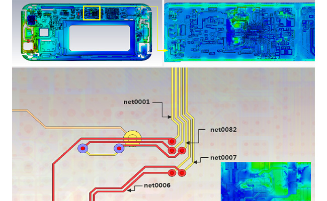
The same concept is now applied to a real world smart phone. Figure 11 illustrates the results when the diversity antenna is excited. H-field maps allows to identify critical regions, such as net0001, net0082, net 0007 and net0006. These lines are routed on top of a region with higher current density, thus they can be critical for coupling to the antenna and should be further analyzed.
By employing this method, we can predict that RFI is critical for a SD clock net. This is instead of a high-speed signal routed from the AP to the top part of the phone, which was originally used to analyze the coupling to the antenna, because it was suspected as being the possible cause of a RFI/desense issue.
This can be clearly seen in the S-parameters in Figure 10b where we observe coupling values below -80dB for the high-speed net, whereas the coupling to the SD clock net is much higher. Furthermore, the frequency domain spectrum reveals important resonances, some of them being very close to the GSM band.
To verify this, NFS measurements are performed monitoring the SD card region. Results are reported in Figure 12, and they clearly reveal EMI issues in the frequency range 0.8-0.85GHz. This can be observed during the on-the-GO (OTG) activity with both assembled and di-assembled phone.


Figure 11. a): Real world smart phone model: H-field distribution when diversity antenna is excited, signal identification and layer by layer map, b): RFI coupling antenna to signal lines
Near-field probes with 1mm resolution (similarly to the NFS) are used in the numerical model to register the E-field on the SD card. Figure 13 shows the amplitude value of the E-field for the probes. A peak at 0.84 GHz can be seen, which is very close to the resonance being detected by the NFS measurement. This experiment further confirms the feasibility of the proposed methodology for RFI analysis in mobile devices.

Figure 12. Measurement set-up for the near field scan test with map of the nearfield in the SD card area at 0.8GHz for assembled and disassembled phone case

Figure 13. Electromagnetic model of the phone with in evidence the probe location 1mm above the SD card and E-field amplitude
Conclusions
A methodology to predict RFI at an early design stage in mobile devices is introduced. The main idea is to use numerically generated H-field maps when the antennas inside the phone are excited. Critical regions on the PCB can be identified, thus reducing the number of experiments aimed to analyze the signals to antenna.
The method is based on the reciprocity principle, and it shows a good estimation of the signal to antenna coupling paths which can generate desense problems. A real-world test case is used to validate the methodology showing qualitative correlation with near field scan measurement.
An earlier version of this paper was a DesignCon 2017 Best Paper Award Winner.
References
1. USB 3.0 Radio Frequency Interference Impact on 2.4 GHz Wireless Devices, White Paper from Intel, April 2012, Available at
http://www.usb.org/developers/whitepapers/327216.pdf
2. Jinkyu Bang, Young Lee, Yongsup Kim and Austin S. Kim, “Calculation of total isotropic sensitivity considering digital harmonic noise of mobile phone”, on Proc. of IEEE 2009
3. E.X. Alban, S. Sajuyigbe, H. Skinner, A. Alcocer, R. Camacho, “Mitigation Techniques for RFI due to Broadband Noise”, on Proc. of IEEE Int. Symposium on EMC, 4-8 August 2014
4. H. Shim, J. Lee, “Interference Issues of Smartphones and Challenges to Model Noise from Chipsets”, on Proc. of URSI ASIA Pacific radio Conference, August 21-25, 2016, Seoul, South Korea.
5. J.J. Kim, K.M. Yang, J.M. Kim, Y.J. Kim and S.Y. Lee, “Methodology for RF receiver sensitivity analysis using electromagnetic field map”, ELECTRONICS LETTERS 6th November 2014 Vol. 50 No. 23 pp. 1753–1755
6. Jin-Sung Youn, et al, “ Chip and package level wideband EMI analysis for mobile DRAM devices”, on Proceedings of DesignCon 2016
7. H. Wang, V. Khilkevich, Y. J. Zhang, and J. Fan, “Estimating radio-frequency interference to an antenna due to near-field coupling using decomposition method based on reciprocity,” IEEE Trans. Electromagnetic Compatibility, vol. 55, no. 6, pp. 1125- 1131, 2013
8. O. Franek, M. Sorensen, H. Ebert, and G. F. Pedersen, "Influence of nearby obstacles on the feasibility of a Huygens box as a field source," in IEEE Int. Symposium Electromagnetic Compatibility, pp. 600-604, 2012.
9. J. Pan, H. Wang, X. Gao, C. Hwang, E. Song, H.-B. Park, and J. Fan, “Radio-Frequency Interference Estimation Using Equivalent Dipole-Moment Models and Decomposition Method Based on Reciprocity”, on IEEE Trans. on Electromagnetic Compatibility, vol.58, no.6, pp 75-84, Dec. 2015.
10. Seil Kim, Sungwook Moon, Seungbae Lee, Donny Yi, et al., “Simulation based analysis on EMI effect in LPDDR interface for mitigating RFI in a mobile environment”, on Proc. of EPEPS 2016
Author(s) Biography
Antonio Ciccomancini Scogna is currently working as principal engineer with Samsung Electronics (HE-Group). His interest includes Signal and Power Integrity (SIPI), EMC/EMI and RFI/desense for mobile devices. He has more than 15 years of experience in the field of EM simulation for SIPI, EDA and hardware industry, including Computer Simulation Technology (CST) and Apple. He has more than 150 publications in IEEE Journal Transactions, Conference Proceedings and relevant EDA magazines. He is active member of IEEE EMC Society where he serves as Associate Editor and he is chair of TC10 subcommittee for EM co-simulation.
Hwanwoo Shim is a principal engineer at Mobile Communication Business Division, Samsung Electronics. He has been working as a leader of CAE application team after more than ten years of experience as a project leader for commercial smartphone development. His technical interests include SI/PI simulations and noise modeling techniques to estimate EMI/RFI issues in early design stages. He received Ph.D. from Missouri S&T EMC laboratory and M.S. from Korea Advanced Institute of Science and Technology (KAIST), Daejeon Korea.
Jiheon Yu is working as principal engineer with Samsung Electronics (HE-group), Suwon-Si, South Korea
Chang-Yong Oh is working as senior engineer with Samsung Electronics (HE-group), Suwon-Si, South Korea
Seyoon Cheon is working as assistant engineer with Samsung Electronics (HE-group), Suwon-Si, South Korea
NamSeok Oh is working as senior engineer with Samsung Electronics (HE-group), Suwon-Si, South Korea