
Catalog
| I. General Introduction | 1. Cascode Amplifier Circuit |
| 2. Folded Cascode Amplifier | |
| II. Features | 1. Frequency Response |
| 2. Stability | |
| 3. Advantages and Disadvantages |
An analog circuit's output is increased by using a cascode amplifier. The use of cascode is a common approach that can be extended to both transistor and vacuum tube applications. In the year 1939, the tern cascode was included in an article written by Roger Wayne Hickman and Frederick Vinton Hunt. The subject at hand is the use of voltage stabilizers. They constructed a cascode for two triodes, with the first using a common cathode configuration and the second using a common grid as a pentode substitution. As a consequence, the name can be translated as a reduction of cascaded triodes with pentode-like characteristics.
I. General Introduction of Cascode Amplifier
The cascode amplifier is split into two stages: a CE (common-emitter) stage and a CB (common-base) stage, with the CE feeding the CB. As opposed to a single stage of an amplifier, the mixture of both will have multiple properties such as high input/output separation, high i/p impedance, high o/p impedance, and high bandwidth.
This amplifier is commonly used in current circuits by using two transistors, either BJTs or FETs. One transistor acts as a CE, or common source, while the others act as a CB, or common gate. Since there is no direct coupling from the o/p to the i/p, this amplifier increases i/o separation, eliminates the miller effect, and hence provides high bandwidth.
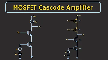
1. Cascode Amplifier Circuit
The input step of a field-effect transistor is a FET CS amplifier, and Vin voltage is applied to the transistor's gate terminal. The output phase, on the other hand, is the FET CG amplifier that is powered by the input phase. Rd is the drain resistance for the output step, and Vout is the output voltage collected from Q2. Since Q2 is grounded in the circuit, the drain voltage in FET Q1 and the source voltage in FET Q2 are kept constant. This means that FET Q2 has the lowest input resistance for FET Q1. Low input resistance for Q1 decreases gain and Miller effect values, resulting in an increase in bandwidth level indirectly.
The reduction in FET Q1 gain has little effect on the circuit's total gain because FET Q2 compensates for it. Since discharge and charges from the drain terminal to the source stray capacitance are conducted via the Rd, the Miller effect has little effect on FET Q2, and the frequency response and load values are only disrupted for elevated frequency ranges. The output values of the cascode amplifier are totally isolated from the input values in the circuit architecture. Q1 has fixed voltage levels at the source and drain terminals, while Q2 has fixed voltage levels at the gate and source terminals. The following is a circuit diagram for a FET-operated cascode amplifier:

The FET-based Cascode amplifier circuit is shown below. The Vin (input voltage) is attached to the gate terminal of this amplifier's input stage, which is a typical source of FET. This amplifier's output stage is a typical gate FET with an ambitious input step. The o/p stage's drain resistance is Rd, and the Vout (output voltage) can be calculated at the drain terminal of the secondary transistor.
Since the gate terminal of the Q2 transistor is grounded, the source and drain voltages of the transistors are kept unchanged. That is, the higher Q2 transistor has a low i/p resistance in the direction of the lower Q1 transistor. As a result, the lower transistor's gain is diminished, and the Miller effect is reduced as well. The bandwidth of SO would increase.
The lower transistor's gain loss has little effect on the overall gain since the upper transistor compensates for it. The Miller effect would not affect the upper transistor since the drain resistor should be used to charge and discharge the drain to source drift capacitance. For high frequencies, both the frequency response and the load were affected.
The output of this circuit can be separated from the input. The lower transistor has an approximately stable voltage at its source and drain terminals, while the higher transistor has nearly stable voltage at both terminals. There is practically no input from the o/p to the i/p. As a consequence, the two terminals are well separated using a secure voltage middle relation.
2. Folded Cascode Amplifier
This is a single-stage amplifier in which the typical source transistor is cas0ded with the reverse polarity CB transistor. In this circuit, the input segment is a variable pair that serves as a CS stage for the cascode. The two transistor drains are attached to CG transistors with reverse polarity. The CG transistors are then connected to the complex current source, and the circuit is complete.
Gain increment in a multi-stage amplifier can be accomplished due to the constructional nature of this amplifier. By folding the cascode into reverse polarity transistors, the circuit size can be held to a minimum while retaining circuit output and requiring reduced supply voltage. The output resistance value of the circuits can be improved using cascode transistors, which increases the amplifier signal gain. This is the folded cascode amplifier's key benefit.
II. Features of Cascode Amplifier
1. Frequency Response of Cascode Amplifier
The output responses are inverted in correspondence with the input in the cascode amplifier frequency response. They deliver improved amplitude outputs by implementing either cascode or common-emitter amplifiers. The cascode amplifier signal is three times greater than the predicted range as compared to a CE signal.
2. Stability of Cascode Amplifier
Another noteworthy characteristic of the cascode amplifier that must be addressed is its reliability. The cascode constructional architecture is a safe arrangement in and of itself. The lower transistor has a nearly constant voltage level at the source and drain terminals, so there isn't anything to create gate feedback. The upper transistor, on the other hand, retains a steady voltage level at the source and gate terminals. As a consequence, the only nodes with matching voltage levels are the output and reference nodes.
3. Advantages and Disadvantages of Cascode Amplifier
Advantages
Increased gain, reliability, better impedance ratios, more bandwidth levels, and slew rate are all characteristics of the cascode circuit.
The circuit's construction is incredibly basic.
In superheterodyne receivers, the cascode amplifier is implemented as a multiplication mixer. The oscillator signal is fed to the upper gate, while the RF signal is fed to the lower gate. So all of these signals are compounded, and the IF is used as the mixer-upper amplifier's drain.
Disadvantages
Two transistors with a high voltage supply are necessary for this amplifier. Two transistors should be biased by ample VDS in the process for the two-transistor cascode, setting a lower limit on the voltage supply.


")


