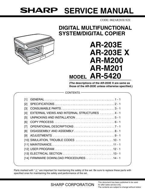
service manual ar-203e ar-203e x ar-m200 ar-m201 model ar-5420
service manual ar-203e ar-203e x ar-m200 ar-m201 model ar-5420
service manual ar-203e ar-203e x ar-m200 ar-m201 model ar-5420

Create successful ePaper yourself
Turn your PDF publications into a flip-book with our unique Google optimized e-Paper software.
SERVICE MANUAL<br />
CONTENTS<br />
P<strong>ar</strong>ts m<strong>ar</strong>ked with “ ” <strong>ar</strong>e important for maintaining the safety of the set. Be sure to replace these p<strong>ar</strong>ts with<br />
specified ones for maintaining the safety and performance of the set.<br />
SHARP CORPORATION<br />
CODE: 00ZAR203E/S2E<br />
DIGITAL MULTIFUNCTIONAL<br />
SYSTEM/DIGITAL COPIER<br />
AR-203E<br />
AR-203E X<br />
AR-M200<br />
AR-M201<br />
MODEL AR-<strong>5420</strong><br />
(The descriptions of the AR-203E X <strong>ar</strong>e same as<br />
those of the AR-203E unless otherwise specified.)<br />
[1] GENERAL . . . . . . . . . . . . . . . . . . . . . . . . . . . . . . . . . . . . . . . . . . . 1 - 1<br />
[2] SPECIFICATIONS . . . . . . . . . . . . . . . . . . . . . . . . . . . . . . . . . . . . . 2 - 1<br />
[3] CONSUMABLE PARTS . . . . . . . . . . . . . . . . . . . . . . . . . . . . . . . . . 3 - 1<br />
[4] EXTERNAL VIEWS AND INTERNAL STRUCTURES . . . . . . . . . 4 - 1<br />
[5] UNPACKING AND INSTALLATION . . . . . . . . . . . . . . . . . . . . . . . . 5 - 1<br />
[6] COPY PROCESS . . . . . . . . . . . . . . . . . . . . . . . . . . . . . . . . . . . . . 6 - 1<br />
[7] OPERATIONAL DESCRIPTIONS . . . . . . . . . . . . . . . . . . . . . . . . . 7 - 1<br />
[8] DISASSEMBLY AND ASSEMBLY . . . . . . . . . . . . . . . . . . . . . . . . . 8 - 1<br />
[9] ADJUSTMENTS . . . . . . . . . . . . . . . . . . . . . . . . . . . . . . . . . . . . . . 9 - 1<br />
[10] SIMULATION, TROUBLE CODES . . . . . . . . . . . . . . . . . . . . . . . 10 - 1<br />
[11] MAINTENANCE. . . . . . . . . . . . . . . . . . . . . . . . . . . . . . . . . . . . . . 11 - 1<br />
[12] USER PROGRAM . . . . . . . . . . . . . . . . . . . . . . . . . . . . . . . . . . . . 12 - 1<br />
[13] ELECTRICAL SECTION . . . . . . . . . . . . . . . . . . . . . . . . . . . . . . . 13 - 1<br />
[14] FIRMWARE DOWNLOAD PROCEDURES . . . . . . . . . . . . . . . . . 14 - 1<br />
This document has been published to be used<br />
for after sales <strong>service</strong> only.<br />
The contents <strong>ar</strong>e subject to change without notice.
CAUTION<br />
This product is a class 1 laser product that complies with 21CFR 1040 of the CDRH stand<strong>ar</strong>d and<br />
IEC825. This means that this machine does not produce haz<strong>ar</strong>dous laser radiation. The use of controls,<br />
adjustments or performance of procedures other than those specified herein may result in haz<strong>ar</strong>dous<br />
radiation exposure.<br />
This laser radiation is not a danger to the skin, but when an exact focusing of the laser beam is achieved<br />
on the eye’s retina, there is the danger of spot damage to the retina.<br />
The following cautions must be observed to avoid exposure of the laser beam to your eyes at the time of<br />
servicing.<br />
1) When a problem in the laser optical unit has occurred, the whole optical unit must be exchanged as a<br />
unit, not as individual p<strong>ar</strong>ts.<br />
2) Do not look into the machine with the main switch turned on after removing the developer unit, toner<br />
c<strong>ar</strong>tridge, and drum c<strong>ar</strong>tridge.<br />
3) Do not look into the laser beam exposure slit of the laser optical unit with the connector connected<br />
when removing and installing the optical system.<br />
4) The middle frame contains the safety interlock switch.<br />
Do not defeat the safety interlock by inserting wedges or other items into the switch slot.<br />
LASER WAVE – LENGTH : 770 ~ 795nm<br />
Pulse times : 12.88µs ± 12.88ns/7mm<br />
Out put power : MAX 0.2mW<br />
CAUTION<br />
INVISIBLE LASER RADIATION,<br />
WHEN OPEN AND INTERLOCKS DEFEATED.<br />
AVOID EXPOSURE TO BEAM.<br />
VORSICHT<br />
UNSICHTBARE LASERSTRAHLUNG,<br />
WENN ABDECKUNG GEÖFFNET UND<br />
SICHERHEITSVERRIEGELUNG ÜBERBRÜCKT.<br />
NICHT DEM STRAHL AUSSETZEN.<br />
VARO !<br />
AVATTAESSA JA SUOJALUKITUS<br />
OHITETTAESSA OLET ALTTIINA<br />
NÄKYMÄTTÖMÄLLE LASERSÄTEILYLLE ÄLÄ<br />
KATSO SÄTEESEEN.<br />
ADVARSEL<br />
USYNLIG LASERSTRÅLNING VED ÅBNING, NÅR<br />
SIKKERHEDSBRYDERE ER UDE AF<br />
FUNKTION. UNDGÅ UDSAETTELSE FOR<br />
STRÅLNING.<br />
VARNING !<br />
OSYNLIG LASERSTRÅLNING NÄR DENNA DEL<br />
ÄR ÖPPNAD OCH SPÄRREN ÄR URKOPPLAD.<br />
BETRAKTA EJ STRÅLEN. – STRÅLEN ÄR<br />
FARLIG.
At the production line, the output power<br />
of the scanner unit is adjusted to 0.18<br />
MILLI-WATT PLUS 20 PCTS and is<br />
maintained constant by the operation of<br />
the Automatic Power Control (APC).<br />
Even if the APC circuit fails in operation<br />
for some reason, the maximum output<br />
power will only be 15 MILLI-WATT 0.1<br />
MICRO-SEC. Giving and accessible<br />
emission level of 42 MICRO-WATT<br />
which is still-less than the limit of<br />
CLASS-1 laser product.<br />
The foregoing is applicable only to the 220V<br />
<strong>model</strong>, 230V <strong>model</strong> and 240V <strong>model</strong>.<br />
Caution<br />
This product contains a low power laser<br />
device. To ensure continued safety do not<br />
remove any cover or attempt to gain access<br />
to the inside of the product. Refer all<br />
servicing to qualified personnel.<br />
VAROITUS! LAITTEEN KÄYTTÄMINEN MUULLA<br />
KUIN TÄSSÄ KÄYTTÖOHJEESSA MAINITULLA<br />
TAVALLA SAATTAA ALTISTAA KÄYTTÄJÄN<br />
TURVALLISUUSLUOKAN 1 YLITTÄVÄLLE<br />
NÄKYMÄTTÖMÄLLE LASERSÄTEILYLLE.<br />
VARNING - OM APPARATEN ANVÄNDS PÅ ANNAT<br />
SÄTT ÄN I DENNA BRUKSANVISNING<br />
SPECIFICERATS, KAN ANVÄNDAREN UTSÄTTAS<br />
FÖR OSYNLIG LASERSTRÅLNING, SOM<br />
ÖVERSKRIDER GRÄNSEN FÖR LASERKLASS 1.<br />
LUOKAN 1 LASERLAITE<br />
KLASS 1 LASER APPARAT
[1] GENERAL<br />
1. Major functions . . . . . . . . . . . . . . . . . . . . . . . . . . . . . . . 1-1<br />
[2] SPECIFICATIONS<br />
1. Basic Specifications . . . . . . . . . . . . . . . . . . . . . . . . . . . 2-1<br />
2. Operation specifications . . . . . . . . . . . . . . . . . . . . . . . . 2-1<br />
3. Copy performance . . . . . . . . . . . . . . . . . . . . . . . . . . . . 2-2<br />
4. GDI printer (AR-203E only). . . . . . . . . . . . . . . . . . . . . . 2-3<br />
5. SPLC printer (AR-M200/M201). . . . . . . . . . . . . . . . . . . 2-3<br />
6. Scan function (AR-203E/M200/M201) . . . . . . . . . . . . . 2-3<br />
[3] CONSUMABLE PARTS<br />
1. Supply system table . . . . . . . . . . . . . . . . . . . . . . . . . . . 3-1<br />
A. Europe Subsidi<strong>ar</strong>y (AR-203E/<strong>5420</strong>/M200/M201),<br />
SCA/SCNZ (AR-203E/M201) . . . . . . . . . . . . . . . . . . 3-1<br />
B. Asia Subsidi<strong>ar</strong>y (AR-203E/M201). . . . . . . . . . . . . . . 3-1<br />
C. SMEF/Distributor (AR-203E/M201) . . . . . . . . . . . . . 3-1<br />
D. SRH (AR-203E/M201) . . . . . . . . . . . . . . . . . . . . . . . 3-1<br />
2. Environmental. . . . . . . . . . . . . . . . . . . . . . . . . . . . . . . . 3-2<br />
3. Production control number (lot No.) identification. . . . . 3-2<br />
4. Toner c<strong>ar</strong>tridge replacement. . . . . . . . . . . . . . . . . . . . . 3-3<br />
[4] EXTERNAL VIEWS AND INTERNAL STRUCTURES<br />
1. Appe<strong>ar</strong>ance . . . . . . . . . . . . . . . . . . . . . . . . . . . . . . . . . 4-1<br />
2. Internal . . . . . . . . . . . . . . . . . . . . . . . . . . . . . . . . . . . . . 4-1<br />
3. Operation panel . . . . . . . . . . . . . . . . . . . . . . . . . . . . . . 4-2<br />
A. AR-203E/<strong>5420</strong> . . . . . . . . . . . . . . . . . . . . . . . . . . . . . 4-2<br />
B. AR-M200/M201 . . . . . . . . . . . . . . . . . . . . . . . . . . . . 4-3<br />
4. Motors and solenoids . . . . . . . . . . . . . . . . . . . . . . . . . . 4-5<br />
5. Sensors and switches. . . . . . . . . . . . . . . . . . . . . . . . . . 4-6<br />
6. PWB unit. . . . . . . . . . . . . . . . . . . . . . . . . . . . . . . . . . . . 4-7<br />
7. Cross sectional view . . . . . . . . . . . . . . . . . . . . . . . . . . . 4-8<br />
[5] UNPACKING AND INSTALLATION<br />
1. Copier installation . . . . . . . . . . . . . . . . . . . . . . . . . . . . . 5-1<br />
2. Cautions on handling . . . . . . . . . . . . . . . . . . . . . . . . . . 5-1<br />
3. Checking packed components and accessories. . . . . . 5-1<br />
4. Unpacking. . . . . . . . . . . . . . . . . . . . . . . . . . . . . . . . . . . 5-2<br />
5. Removing protective packing materials . . . . . . . . . . . . 5-2<br />
6. Developer unit installation. . . . . . . . . . . . . . . . . . . . . . . 5-2<br />
7. Toner c<strong>ar</strong>tridge installation . . . . . . . . . . . . . . . . . . . . . . 5-3<br />
8. Loading paper. . . . . . . . . . . . . . . . . . . . . . . . . . . . . . . . 5-4<br />
9. Power to copier. . . . . . . . . . . . . . . . . . . . . . . . . . . . . . . 5-4<br />
[6]<br />
10. Softw<strong>ar</strong>e (AR-203E/M200/M201) . . . . . . . . . . . . . . . . . 5-4<br />
A. Before installation. . . . . . . . . . . . . . . . . . . . . . . . . . . 5-4<br />
B. Installing the softw<strong>ar</strong>e. . . . . . . . . . . . . . . . . . . . . . . . 5-5<br />
C. Setting up Button Manager. . . . . . . . . . . . . . . . . . . . 5-7<br />
11. Interface . . . . . . . . . . . . . . . . . . . . . . . . . . . . . . . . . . . . 5-9<br />
A. USB . . . . . . . . . . . . . . . . . . . . . . . . . . . . . . . . . . . . . 5-9<br />
12. Moving . . . . . . . . . . . . . . . . . . . . . . . . . . . . . . . . . . . . . 5-9<br />
13. Scanner moisture-proof kit . . . . . . . . . . . . . . . . . . . . . . 5-9<br />
A. Components . . . . . . . . . . . . . . . . . . . . . . . . . . . . . . . 5-9<br />
B. Precautions at installation . . . . . . . . . . . . . . . . . . . . 5-9<br />
C. Attachment method . . . . . . . . . . . . . . . . . . . . . . . . . 5-9<br />
COPY PROCESS<br />
1. Functional diagram . . . . . . . . . . . . . . . . . . . . . . . . . . . . 6-1<br />
2. Outline of print process. . . . . . . . . . . . . . . . . . . . . . . . . 6-2<br />
3. Actual print process . . . . . . . . . . . . . . . . . . . . . . . . . . . 6-2<br />
CONTENTS<br />
[7] OPERATIONAL DESCRIPTIONS<br />
1. Outline of operation. . . . . . . . . . . . . . . . . . . . . . . . . . . .7-1<br />
2. Scanner section . . . . . . . . . . . . . . . . . . . . . . . . . . . . . .7-2<br />
A. Scanner unit . . . . . . . . . . . . . . . . . . . . . . . . . . . . . . . 7-2<br />
B. Optical system . . . . . . . . . . . . . . . . . . . . . . . . . . . . .7-2<br />
C. Drive system. . . . . . . . . . . . . . . . . . . . . . . . . . . . . . .7-2<br />
3. Laser unit . . . . . . . . . . . . . . . . . . . . . . . . . . . . . . . . . . .7-3<br />
A. Basic structure . . . . . . . . . . . . . . . . . . . . . . . . . . . . .7-3<br />
B. Laser beam path. . . . . . . . . . . . . . . . . . . . . . . . . . . . 7-3<br />
C. Composition . . . . . . . . . . . . . . . . . . . . . . . . . . . . . . .7-3<br />
4. Fuser section . . . . . . . . . . . . . . . . . . . . . . . . . . . . . . . .7-3<br />
A. General description . . . . . . . . . . . . . . . . . . . . . . . . . 7-4<br />
5. Paper feed section and paper transport section . . . . . . 7-4<br />
A. Paper transport path and general operations . . . . . . 7-4<br />
6. D-D (Duplex to Duplex) mode paper/<br />
document transport (Duplex <strong>model</strong>)<br />
(AR-M201 only). . . . . . . . . . . . . . . . . . . . . . . . . . . . . . . 7-7<br />
A. Initial state . . . . . . . . . . . . . . . . . . . . . . . . . . . . . . . .7-7<br />
B. Front copy. . . . . . . . . . . . . . . . . . . . . . . . . . . . . . . . .7-7<br />
C. Back copy . . . . . . . . . . . . . . . . . . . . . . . . . . . . . . . . .7-7<br />
7. Shifter (AR-M200/M201) . . . . . . . . . . . . . . . . . . . . . . . .7-8<br />
[8] DISASSEMBLY AND ASSEMBLY<br />
1. High voltage section . . . . . . . . . . . . . . . . . . . . . . . . . . . 8-1<br />
A. List . . . . . . . . . . . . . . . . . . . . . . . . . . . . . . . . . . . . . .8-1<br />
B. Drum replacement . . . . . . . . . . . . . . . . . . . . . . . . . .8-1<br />
C. Disassembly procedure . . . . . . . . . . . . . . . . . . . . . . 8-3<br />
D. Assembly procedure. . . . . . . . . . . . . . . . . . . . . . . . .8-3<br />
E. Ch<strong>ar</strong>ger wire cleaning. . . . . . . . . . . . . . . . . . . . . . . .8-4<br />
F. Ch<strong>ar</strong>ger wire replacement . . . . . . . . . . . . . . . . . . . .8-4<br />
2. Operation panel section . . . . . . . . . . . . . . . . . . . . . . . . 8-4<br />
A. List . . . . . . . . . . . . . . . . . . . . . . . . . . . . . . . . . . . . . .8-4<br />
B. Disassembly procedure . . . . . . . . . . . . . . . . . . . . . . 8-4<br />
C. Assembly procedure. . . . . . . . . . . . . . . . . . . . . . . . .8-5<br />
3. Optical section . . . . . . . . . . . . . . . . . . . . . . . . . . . . . . .8-5<br />
A. List . . . . . . . . . . . . . . . . . . . . . . . . . . . . . . . . . . . . . .8-5<br />
B. Disassembly procedure . . . . . . . . . . . . . . . . . . . . . . 8-5<br />
C. Assembly procedure. . . . . . . . . . . . . . . . . . . . . . . . .8-7<br />
4. Fusing section. . . . . . . . . . . . . . . . . . . . . . . . . . . . . . . .8-7<br />
A. List . . . . . . . . . . . . . . . . . . . . . . . . . . . . . . . . . . . . . .8-7<br />
B. Disassembly procedure . . . . . . . . . . . . . . . . . . . . . . 8-7<br />
C. Assembly procedure. . . . . . . . . . . . . . . . . . . . . . . .8-10<br />
5. Tray paper feed/transport section . . . . . . . . . . . . . . . . 8-10<br />
A. List . . . . . . . . . . . . . . . . . . . . . . . . . . . . . . . . . . . . .8-10<br />
B. Disassembly procedure . . . . . . . . . . . . . . . . . . . . . 8-10<br />
C. Assembly procedure. . . . . . . . . . . . . . . . . . . . . . . .8-16<br />
6. Manual paper feed section . . . . . . . . . . . . . . . . . . . . . 8-16<br />
A. List . . . . . . . . . . . . . . . . . . . . . . . . . . . . . . . . . . . . .8-16<br />
B. Disassembly procedure . . . . . . . . . . . . . . . . . . . . . 8-16<br />
C. Assembly procedure. . . . . . . . . . . . . . . . . . . . . . . .8-18<br />
D. Pressure plate holder attachment. . . . . . . . . . . . . .8-18<br />
7. Re<strong>ar</strong> frame section . . . . . . . . . . . . . . . . . . . . . . . . . . .8-18<br />
A. List . . . . . . . . . . . . . . . . . . . . . . . . . . . . . . . . . . . . .8-18<br />
B. Disassembly procedure . . . . . . . . . . . . . . . . . . . . . 8-18<br />
C. Assembly procedure. . . . . . . . . . . . . . . . . . . . . . . .8-19
8 Power section . . . . . . . . . . . . . . . . . . . . . . . . . . . . . . . 8-20<br />
A. List . . . . . . . . . . . . . . . . . . . . . . . . . . . . . . . . . . . . . 8-20<br />
B. Disassembly procedure . . . . . . . . . . . . . . . . . . . . . 8-20<br />
C. Assembly procedure. . . . . . . . . . . . . . . . . . . . . . . . 8-20<br />
9. DV unit section . . . . . . . . . . . . . . . . . . . . . . . . . . . . . . 8-20<br />
A. Developer . . . . . . . . . . . . . . . . . . . . . . . . . . . . . . . . 8-20<br />
B. DV seal. . . . . . . . . . . . . . . . . . . . . . . . . . . . . . . . . . 8-20<br />
C. DV blade. . . . . . . . . . . . . . . . . . . . . . . . . . . . . . . . . 8-21<br />
D. DV doctor . . . . . . . . . . . . . . . . . . . . . . . . . . . . . . . . 8-21<br />
E. DV sensor. . . . . . . . . . . . . . . . . . . . . . . . . . . . . . . . 8-21<br />
10. Duplex motor section (AR-M201 only) . . . . . . . . . . . . 8-21<br />
A. List . . . . . . . . . . . . . . . . . . . . . . . . . . . . . . . . . . . . . 8-21<br />
B. Disassembly procedure . . . . . . . . . . . . . . . . . . . . . 8-21<br />
C. Assembly procedure. . . . . . . . . . . . . . . . . . . . . . . . 8-21<br />
11. Reverse roller section (AR-M201 only). . . . . . . . . . . . 8-22<br />
A. List . . . . . . . . . . . . . . . . . . . . . . . . . . . . . . . . . . . . . 8-22<br />
B. Disassembly procedure . . . . . . . . . . . . . . . . . . . . . 8-22<br />
C. Assembly procedure. . . . . . . . . . . . . . . . . . . . . . . . 8-22<br />
[9] ADJUSTMENTS<br />
1. Optical section . . . . . . . . . . . . . . . . . . . . . . . . . . . . . . . 9-1<br />
A. Copy magnification ratio adjustment . . . . . . . . . . . . 9-1<br />
B. Image position adjustment . . . . . . . . . . . . . . . . . . . . 9-2<br />
2. Copy density adjustment . . . . . . . . . . . . . . . . . . . . . . . 9-4<br />
A. Copy density adjustment timing . . . . . . . . . . . . . . . . 9-4<br />
B. Note for copy density adjustment . . . . . . . . . . . . . . . 9-4<br />
C. Necess<strong>ar</strong>y tool for copy density adjustment. . . . . . . 9-4<br />
D. Features of copy density adjustment . . . . . . . . . . . . 9-4<br />
E. Copy density adjustment procedure. . . . . . . . . . . . . 9-5<br />
3. High voltage adjustment . . . . . . . . . . . . . . . . . . . . . . . . 9-5<br />
A. Main ch<strong>ar</strong>ger (Grid bias). . . . . . . . . . . . . . . . . . . . . . 9-5<br />
B. DV bias check . . . . . . . . . . . . . . . . . . . . . . . . . . . . . 9-6<br />
4. Duplex adjustment . . . . . . . . . . . . . . . . . . . . . . . . . . . . 9-6<br />
A. Adjusting the paper reverse position in memory<br />
for duplex copying (AR-M200/M201) . . . . . . . . . . . . 9-6<br />
B. Adjusting trailing edge void in duplex copy mode<br />
(AR-M201) . . . . . . . . . . . . . . . . . . . . . . . . . . . . . . . . 9-6<br />
5. Automatic black level correction . . . . . . . . . . . . . . . . . . 9-7<br />
[10] SIMULATION, TROUBLE CODES<br />
1. Entering the simulation mode . . . . . . . . . . . . . . . . . . . 10-1<br />
2. Key rule. . . . . . . . . . . . . . . . . . . . . . . . . . . . . . . . . . . . 10-1<br />
3. List of simulations . . . . . . . . . . . . . . . . . . . . . . . . . . . . 10-1<br />
4. Descriptions of v<strong>ar</strong>ious simulations. . . . . . . . . . . . . . . 10-3<br />
5. Trouble codes . . . . . . . . . . . . . . . . . . . . . . . . . . . . . . 10-40<br />
A. Trouble codes list . . . . . . . . . . . . . . . . . . . . . . . . . 10-40<br />
B. Details of trouble codes . . . . . . . . . . . . . . . . . . . . 10-41<br />
[11] MAINTENANCE<br />
1. Maintenance table . . . . . . . . . . . . . . . . . . . . . . . . . . . 11-1<br />
2. Maintenance display system. . . . . . . . . . . . . . . . . . . . 11-1<br />
3. Remaining toner indication . . . . . . . . . . . . . . . . . . . . . 11-1<br />
[12] USER PROGRAM<br />
1. Functions that can be set with user programs . . . . . . 12-1<br />
2. Toner save mode (AR-203E/<strong>5420</strong>). . . . . . . . . . . . . . . 12-1<br />
3. User programs (AR-203E/<strong>5420</strong>) . . . . . . . . . . . . . . . . . 12-1<br />
4. User programs (AR-M200/M201) . . . . . . . . . . . . . . . . 12-2<br />
A. Copy mode . . . . . . . . . . . . . . . . . . . . . . . . . . . . . . . 12-3<br />
B. Print mode . . . . . . . . . . . . . . . . . . . . . . . . . . . . . . . 12-4<br />
[13] ELECTRICAL SECTION<br />
1. Block diagram . . . . . . . . . . . . . . . . . . . . . . . . . . . . . . .13-1<br />
A. Overall block diagram (AR-203E/<strong>5420</strong>) . . . . . . . . . 13-1<br />
B. Overall block diagram (AR-M200/M201) . . . . . . . . 13-2<br />
2. Actual wiring diagram . . . . . . . . . . . . . . . . . . . . . . . . .13-3<br />
A. MCU PWB (AR-203E/<strong>5420</strong>) . . . . . . . . . . . . . . . . . . 13-3<br />
B. MCU PWB (AR-M200/M201) . . . . . . . . . . . . . . . . . 13-4<br />
C. SPF unit (AR-203E optional only). . . . . . . . . . . . . . 13-5<br />
D. RSPF unit (AR-M200/M201 optional only) . . . . . . . 13-5<br />
E. 2nd cassette unit<br />
(AR-203E/M200/M201 optional only) . . . . . . . . . . . 13-5<br />
F. Network box and FAX<br />
(AR-M200/M201 optional only). . . . . . . . . . . . . . . . 13-6<br />
3. Signal name list. . . . . . . . . . . . . . . . . . . . . . . . . . . . . . 13-6<br />
4. Circuit diagram . . . . . . . . . . . . . . . . . . . . . . . . . . . . . .13-9<br />
A. MCU PWB (AR-203E/<strong>5420</strong>) . . . . . . . . . . . . . . . . . . 13-9<br />
B. MCU PWB (AR-M200/M201) . . . . . . . . . . . . . . . . 13-21<br />
C. OPE PWB (AR-203E/<strong>5420</strong>) . . . . . . . . . . . . . . . . . 13-37<br />
D. OPERATION PWB (AR-M200/M201). . . . . . . . . . 13-38<br />
[14] FIRMWARE DOWNLOAD PROCEDURES<br />
1. Initial setting (Serial number setting procedures) . . . . 14-1<br />
2. Download procedures . . . . . . . . . . . . . . . . . . . . . . . . .14-1<br />
3. Version acquisition procedures. . . . . . . . . . . . . . . . . . 14-3<br />
4. EEPROM data acquisition procedure . . . . . . . . . . . . . 14-4<br />
5. Installing procedures. . . . . . . . . . . . . . . . . . . . . . . . . . 14-5
[1] GENERAL<br />
1. Major functions<br />
Configurations<br />
Item<br />
Model<br />
CPM<br />
(A4)<br />
PPM<br />
(A4)<br />
SB/<br />
MB<br />
2 Tray SPF R-SPF<br />
Color<br />
Scanner<br />
GDI<br />
printer<br />
SPLC<br />
printer<br />
E-<br />
SORT<br />
Duplex Shifter USB RJ45 FAX<br />
External<br />
NIC<br />
AR-203E 20CPM 15PPM MB Opt Opt ✕ ✕ ✕ ✕ ✕<br />
✕ ✕ ✕<br />
AR-<strong>5420</strong> 20CPM — MB ✕ ✕ ✕ ✕ ✕ ✕ ✕ ✕ ✕<br />
(2.0 full)<br />
✕ ✕ ✕ ✕<br />
AR-M200 20CPM 20PPM MB Opt ✕ Opt ✕ ✕<br />
✕ Opt Opt<br />
(2.0 Hi)<br />
AR-M201 20CPM 20PPM MB Opt ✕ Opt ✕<br />
✕ Opt Opt<br />
(2.0 Hi)<br />
Descriptions of items<br />
CPM: Copy speed (Copies Per Minute)<br />
PPM: Print speed (Print Per Minute)<br />
SB/MB: SB = Manual feed single bypass,<br />
MB = Manual feed multi-bypass<br />
2 Tray: Second cassette unit (AR-D33)<br />
SPF: Original feed unit (AR-SP9)<br />
R-SPF: Duplex original feed unit (AR-RP9)<br />
Color Scanner: Color scanner function<br />
GDI printer: GDI printer function with USB.<br />
SPLC printer: SPLC printer function with USB.<br />
E-SORT: Electronic sort function<br />
Duplex: Auto duplex copy/print function<br />
Shifter: Job sep<strong>ar</strong>ator function<br />
USB: Interface port (USB)<br />
RJ45: Interface port (Network)<br />
FAX: FAX function (AR-FX13)<br />
External NIC: AR-NB2A<br />
Descriptions of table<br />
: Stand<strong>ar</strong>d provision<br />
: No function or no option available<br />
Opt: Option<br />
(Options)<br />
AR-RP9<br />
AR-SP9<br />
AR-203E/<strong>5420</strong>/M200/M201 GENERAL 1 - 1<br />
AR-203E/AR-<strong>5420</strong><br />
AR-M200/AR-M201<br />
AR-FX13<br />
AR-D33<br />
AR-NB2A
[2] SPECIFICATIONS<br />
1. Basic Specifications<br />
Item<br />
Type Desktop<br />
Copy system Dry, electrostatic<br />
Segment (class) Digital personal copier<br />
Copier dimensions AR-203E/<strong>5420</strong>: 518mm (W) x 445mm (D) x 298mm (H) (20-1/2" (W) x 17-5/8" (D) x 11-3/4" (H))<br />
AR-M200/M201: 518mm (W) x 452mm (D) x 298mm (H) (20-1/2" (W) x 17-7/8" (D) x 11-3/4" (H))<br />
Weight (Approximately) AR-203E/<strong>5420</strong>: 16.6kg (36.5 lbs.)<br />
AR-M200: 19.8kg (43.7 lbs.)<br />
AR-M201: 20.5kg (45.2 lbs.)<br />
Toner c<strong>ar</strong>tridge not included<br />
2. Operation specifications<br />
Section, item Details<br />
Paper feed Paper feed system 1 tray (250 sheets) + multi-bypass (50 sheets)<br />
section AB system Tray paper feed section Paper size A4, B5, A5 (Landscape)<br />
Paper weight 56 - 80g/m2 Paper feed capacity 250 sheets<br />
Kinds Stand<strong>ar</strong>d paper, specified paper, recycled paper<br />
Rem<strong>ar</strong>k User adjustment of paper guide available<br />
Multi-bypass paper Paper size A4, B5, A5, B6, A6 (Landscape)<br />
feed section<br />
Paper weight 56 - 128g/m2 Paper feed capacity 50 sheets<br />
Kinds Stand<strong>ar</strong>d paper, specified paper, recycled paper, OHP,<br />
Label, Envelop (Single copy)<br />
Rem<strong>ar</strong>k User adjustment of paper guide available<br />
Inch Tray paper feed section Paper size 8-1/2" x 14", 8-1/2" x 11", 8-1/2" x 5-1/2" (Landscape)<br />
system<br />
Paper weight 15 - 21 lbs.<br />
Paper feed capacity 250 sheets<br />
Kinds Stand<strong>ar</strong>d paper, specified paper, recycled paper<br />
Rem<strong>ar</strong>k User adjustment of paper guide available<br />
Multi-bypass paper Paper size 8-1/2" x 14", 8-1/2" x 11", 8-1/2" x 5-1/2", 3-1/2" x 5-1/2"<br />
feed section<br />
(Landscape)<br />
Paper weight 15 - 34.5 lbs.<br />
Paper feed capacity 50 sheets<br />
Kinds Stand<strong>ar</strong>d paper, specified paper, recycled paper, OHP,<br />
Label, Envelop (Single copy)<br />
Rem<strong>ar</strong>k User adjustment of paper guide available<br />
Paper exit section Exit way Face down<br />
Capacity of output tray 200 sheets<br />
Originals Original set Center Registration (left edge)<br />
Max. original size A4 (8-1/2" x 14")<br />
Original kinds sheet, book<br />
Original size detection None<br />
Optical Scanning Scanning system 3 CCDs (RGB) sensor scanning by lighting white lamp<br />
section section CCD sensor Resolution 600 dpi<br />
Lighting lamp Type CCFL<br />
Voltage 560Vrms<br />
Power consumption 2.8W<br />
Output data Output: R, G, B 1 or 8 bits/pixel / Input: A/D 16 bits (12 bits<br />
actual)<br />
Writing Writing system Writing to OPC drum by the semiconductor laser<br />
section Laser unit Resolution 600 dpi<br />
Image forming Photoconductor Type OPC (30ø)<br />
Life 25K<br />
Ch<strong>ar</strong>ger Ch<strong>ar</strong>ging system Saw-tooth ch<strong>ar</strong>ging with a grid, / (-) scorotron disch<strong>ar</strong>ge<br />
Transfer system (+) DC corotron system<br />
Sep<strong>ar</strong>ation system (-) DC corotron system<br />
Developing Developing system Dry, 2-component magnetic brush development system<br />
Cleaning Cleaning system Counter blade system (Counter to rotation)<br />
AR-203E/<strong>5420</strong>/M200/M201 SPECIFICATIONS 2 - 1
Section, item Details<br />
Fusing section Fusing system Heat roller system<br />
Upper heat roller Type Teflon roller<br />
Lower heat roller Type Silicon rubber roller<br />
Heater lamp Type Halogen lamp<br />
Voltage 220 - 240V / 120V<br />
Power consumption 800W<br />
Electrical section Power source Voltage 220 - 240V / 120V<br />
Frequency Common use for 50 and 60Hz<br />
Power consumption Max. Less than 1000W<br />
Average (during copying) AR-203E/<strong>5420</strong>: 350Wh/H or less<br />
AR-M200/ M201: 380Wh/H or less<br />
Average (stand-by) 80Wh/H<br />
Pre-heat mode AR-203E/<strong>5420</strong>: 25Wh/H or less<br />
AR-M200/ M201: 28Wh/H or less<br />
Auto power shut-off mode AR-203E/<strong>5420</strong>: 8.8W or less<br />
AR-M200/ M201: 12.5W or less<br />
3. Copy performance<br />
Section, item Details<br />
Copy magnification Fixed<br />
magnification<br />
ratios<br />
Zooming<br />
magnification<br />
ratios<br />
Manual steps (<strong>manual</strong>, photo) 5 steps<br />
Copy speed First-copy time *2<br />
(Approximately)<br />
AB system<br />
A4 (Landscape)<br />
AB system<br />
B5 (Landscape)<br />
Inch system<br />
8-1/2" x 11"<br />
(Landscape)<br />
Copy speed<br />
(CPM)<br />
Copy speed<br />
(CPM)<br />
Copy speed<br />
(CPM)<br />
AR-203E/<strong>5420</strong>:<br />
3 Reduction + 2 Enl<strong>ar</strong>gement<br />
(AB system: 50, 70, 86, 100, 141, 200%)<br />
(Inch system: 50, 64, 78, 100, 129, 200%)<br />
AR-M200/M201: *1<br />
4 Reduction + 3 Enl<strong>ar</strong>gement<br />
(AB system: 25, 50, 70, 86, 100, 141, 200, 400%)<br />
(Inch system: 25, 50, 64, 78, 100, 129, 200, 400%)<br />
25 - 400% (376 steps in 1% increments)<br />
50 - 200% when using SPF (151 steps in 1% increments)<br />
AR-203E/<strong>5420</strong>:<br />
8.0 seconds (When user program 24 is set to OFF)<br />
10.7 seconds (When user program 24 is set to ON)<br />
AR-M200/M201:<br />
8.0 seconds<br />
(paper: A4 (8-1/2" x 11"), exposure mode: AUTO, copy ratio: 100%)<br />
Same size 20<br />
Enl<strong>ar</strong>gement 20<br />
Reduction 20<br />
Same size 20<br />
Enl<strong>ar</strong>gement 20<br />
Reduction 20<br />
Same size 20<br />
Enl<strong>ar</strong>gement 20<br />
Reduction 20<br />
Max. continuous copy quantity 99<br />
Void Void <strong>ar</strong>ea Leading edge 1 - 4mm<br />
Trailing edge 4mm or less<br />
Side edge 0.5mm or more (per side)<br />
void <strong>ar</strong>ea 4.5mm or less (total of both sides)<br />
Image loss Leading edge same size: 3.0mm or less (OC) / 4mm or less (SPF)<br />
Enl<strong>ar</strong>ge: 1.5mm or less (OC) / 3mm or less (SPF)<br />
Reduction (50%): 6.0mm or less (OC) / 8mm or less (SPF)<br />
W<strong>ar</strong>m-up time 0 sec. Immediately the ready lamp is lit.<br />
Power save mode reset time 0 sec. Immediately the ready lamp is lit.<br />
Paper jam recovery time 0 sec.<br />
∗ Jam recovery condition: Recovery time from 60 sec of door open.<br />
*1: If a value greater than 200% or smaller than 50% is selected when the RSPF is used, the magnification ratio is automatically set to 200% or<br />
50%.<br />
*2: The first-copy time is measured after the power save indicator turns off following power on, using the document glass with the polygon rotating<br />
in the copy ready state and "Selection of copy st<strong>ar</strong>t state" set to ON in the user programs (A4 (8-1/2" x 11"), paper fed from paper tray).<br />
The first-copy time may v<strong>ar</strong>y depending on machine operating conditions and ambient conditions such as temperature.<br />
AR-203E/<strong>5420</strong>/M200/M201 SPECIFICATIONS 2 - 2
4. GDI printer (AR-203E only)<br />
Print speed Max. 15ppm (excluding bypass tray, paper size A4, 8.5" x 11") (V<strong>ar</strong>iable depending on the PC performance)<br />
Duplex No<br />
Memory 8MB<br />
Interface USB 2.0 (Full speed)<br />
Emulation GDI<br />
Resolution 600dpi *1<br />
Supported OS Win 98 / Me / 2000 / XP / Vista<br />
WHQL support Yes *2<br />
*1: Engine Resolution<br />
*2: By running change<br />
5. SPLC printer (AR-M200/M201)<br />
Print speed Max. 20ppm (Paper size: A4, excluding <strong>manual</strong> paper feed)<br />
∗ V<strong>ar</strong>ies depending on the PC performance.<br />
First print time 8 sec. (without data transfer time)<br />
Duplex Yes (AR-M201 only)<br />
ROPM Yes<br />
Memory 64MB<br />
Interface USB2.0 (Hi Speed)<br />
Network Option: Network expansion kit the AR-NB2A<br />
Emulation SPLC (JBIG GDI)<br />
MIB support No<br />
Resolution 600dpi *1<br />
Supported OS Windows 98/Me, Windows 2000 Professional, Windows XP Home Edition/Professional, Windows Vista<br />
WHQL support Yes *2<br />
Application Status window<br />
*1: Engine Resolution<br />
*2: Running change<br />
6. Scan function (AR-203E/M200/M201)<br />
Type Flat Bed Color Scanner<br />
Scanning system Original table/SPF/RSPF<br />
Light source 3 CCDs (RGB) sensor scanning by lighting white lamp (2 pcs of CCFL)<br />
Resolution Optical: 600 x 1200dpi<br />
Setting range: 50 - 9600dpi (Preview resolution is fixed at 75dpi)<br />
Originals Sheet type / Book type<br />
Output data R, G, B 1 or 8 bits/pixel A/D 16 bits (12 bits actual)<br />
Scan range OC/SPF/RSPF: 216mm (H) x 356mm (V) (8.5" (H) x 14.0" (V))<br />
Original position: Left Center<br />
SPF/RSPF position: Right Center<br />
Scan speed OC/SPF: Max. 2.88ms/line<br />
Protocol TWAIN / WIA (Only XP, Vista) / STI<br />
Interface AR-203E: USB2.0 (Full speed support)<br />
AR-M200/M201: USB2.0 (Hi speed support)<br />
Scanner utility Button Manager / Sh<strong>ar</strong>pdesk / Composer<br />
Scan key/lamp Yes<br />
Duplex scan Yes only when the RSPF is installed (AR-M200/M201)<br />
Supported OS Win 98 / Me / 2000 / XP / Vista<br />
Void <strong>ar</strong>ea No<br />
WHQL supported Yes *1<br />
*1: By running change<br />
AR-203E/<strong>5420</strong>/M200/M201 SPECIFICATIONS 2 - 3
[3] CONSUMABLE PARTS<br />
1. Supply system table<br />
A. Europe Subsidi<strong>ar</strong>y (AR-203E/<strong>5420</strong>/M200/M201), SCA/SCNZ (AR-203E/M201)<br />
No. Name Content Life Product name Packing form<br />
1 Toner c<strong>ar</strong>tridge Toner (Toner: Net Weight 243g) × 10 80K<br />
AR-208LT<br />
One c<strong>ar</strong>ton of the<br />
(Black) Polyethylene bag × 10 (8K x 10Pcs) (A4 6% document) AR-208LT includes<br />
10 toner c<strong>ar</strong>tridges.<br />
2 Developer Developer (Developer: Net Weight 170g) × 10 250K<br />
AR-208LD One c<strong>ar</strong>ton of the<br />
(25K x 10Pcs)<br />
AR-208LD includes<br />
10 developers.<br />
3 Drum kit Drum × 1 25K AR-152DM One c<strong>ar</strong>ton of the<br />
Drum fixing plate × 1<br />
collective package<br />
includes 10 units of the<br />
AR-152DM.<br />
B. Asia Subsidi<strong>ar</strong>y (AR-203E/M201)<br />
No. Name Content Life Product name Packing form<br />
1 Toner c<strong>ar</strong>tridge Toner (Toner: Net Weight 243g) × 10 80K<br />
AR-208CT One c<strong>ar</strong>ton of the<br />
(Black) Polyethylene bag × 10 (8K x 10Pcs) (A4 6% document) AR-208CT includes<br />
10 toner c<strong>ar</strong>tridges.<br />
2 Developer Developer (Developer: Net Weight 170g) × 10 250K<br />
AR-208CD One c<strong>ar</strong>ton of the<br />
(25K x 10Pcs)<br />
AR-208CD includes<br />
10 developers.<br />
3 Drum kit Drum × 1 25K AR-152DR One c<strong>ar</strong>ton of the<br />
Drum fixing plate × 1<br />
collective package<br />
includes 10 units of the<br />
AR-152DR.<br />
C. SMEF/Distributor (AR-203E/M201)<br />
No. Name Content Life Product name Packing form<br />
1 Toner c<strong>ar</strong>tridge Toner (Toner: Net Weight 243g) × 10 80K<br />
AR-208ET One c<strong>ar</strong>ton of the<br />
(Black) Polyethylene bag × 10 (8K x 10Pcs) (A4 6% document) AR-208ET includes<br />
10 toner c<strong>ar</strong>tridges.<br />
2 Developer Developer (Developer: Net Weight 170g) × 10 250K<br />
AR-208CD One c<strong>ar</strong>ton of the<br />
(25K x 10Pcs)<br />
AR-208CD includes<br />
10 developers.<br />
3 Drum kit Drum × 1 25K AR-152DR One c<strong>ar</strong>ton of the<br />
Drum fixing plate × 1<br />
collective package<br />
includes 10 units of the<br />
AR-152DR.<br />
D. SRH (AR-203E/M201)<br />
No. Name Content Life Product name Packing form<br />
1 Toner c<strong>ar</strong>tridge Toner (Toner: Net Weight 243g) × 10 80K<br />
AR-208CT-C One c<strong>ar</strong>ton of the<br />
(Black) Polyethylene bag × 10 (8K x 10Pcs) (A4 6% document) AR-208CT-C includes<br />
10 toner c<strong>ar</strong>tridges.<br />
2 Developer Developer (Developer: Net Weight 170g) × 10 250K<br />
AR-208CD-C One c<strong>ar</strong>ton of the<br />
(25K x 10Pcs)<br />
AR-208CD-C includes<br />
10 developers.<br />
3 Drum kit Drum × 1 25K AR-152DR-C One c<strong>ar</strong>ton of the<br />
Drum fixing plate × 1<br />
collective package<br />
includes 10 units of the<br />
AR-152DR-C.<br />
AR-203E/<strong>5420</strong>/M200/M201 CONSUMABLE PARTS 3 - 1
2. Environmental<br />
The environmental conditions for assuring the copy quality and the<br />
machine operations <strong>ar</strong>e as follows:<br />
(1) Normal operating condition<br />
Temperature: 20 - 25°C<br />
Humidity: 65 ± 5%RH<br />
(2) Acceptable operating condition<br />
Humidity (RH)<br />
85%<br />
60%<br />
20%<br />
(3) Transport condition<br />
Humidity (RH)<br />
90%<br />
60%<br />
15%<br />
(4) Supply storage condition<br />
Humidity (RH)<br />
90%<br />
20%<br />
10˚C 30˚C 35˚C<br />
–25˚C 30˚C 40˚C<br />
–5˚C 45˚C<br />
AR-203E/<strong>5420</strong>/M200/M201 CONSUMABLE PARTS 3 - 2<br />
3. Production control number (lot No.)<br />
identification<br />
<br />
Production month<br />
Production day<br />
Destination code<br />
(Dealer, distributor, OEM, etc.)<br />
Production place<br />
(SOCC: Fixed to B.)<br />
End digit of ye<strong>ar</strong><br />
Version No.<br />
<br />
The label on the drum c<strong>ar</strong>tridge shows the date of production.<br />
(SOCC production)<br />
Production month<br />
Production day<br />
Destination code<br />
(Dealer, distributor, OEM, etc.)<br />
Production place<br />
(SOCC: Fixed to B.)<br />
End digit of ye<strong>ar</strong><br />
Version No.<br />
Production control<br />
label attachment position<br />
Production control<br />
label attachment position(*1)<br />
*1: The production control label is not attached to the c<strong>ar</strong>tridge of<br />
a China product.
4. Toner c<strong>ar</strong>tridge replacement<br />
1) Open the front and side cabinets of the copier.<br />
2) Keep holding Toner lever, and<br />
3) C<strong>ar</strong>efully pull out Toner unit from the copier.<br />
2<br />
3<br />
Sub lot<br />
Production day<br />
Production month<br />
End digit of ye<strong>ar</strong><br />
Production place<br />
4) Put Toner unit in a collection bag immediately after removing it<br />
from the copier<br />
Note: Never c<strong>ar</strong>ry exposed Toner unit. Be sure to put it in the collection<br />
bag.<br />
1<br />
AR-203E/<strong>5420</strong>/M200/M201 CONSUMABLE PARTS 3 - 3
[4] EXTERNAL VIEWS AND INTERNAL STRUCTURES<br />
1. Appe<strong>ar</strong>ance<br />
1<br />
2<br />
3<br />
4<br />
5<br />
6<br />
1 Original cover 2 Document glass 3 Operation panel<br />
4 Front cover 5 Paper tray 6 Multi-bypass tray<br />
7 Side cover 8 Side cover open button 9 Bypass tray paper guides<br />
10 Paper output tray 11 Paper output tray extension 12 Power switch<br />
13 Handle 14 Power cord<br />
2. Internal<br />
1<br />
7<br />
8<br />
9<br />
Interface<br />
USB connector<br />
(AR-203E)<br />
Toner c<strong>ar</strong>tridge Drum c<strong>ar</strong>tridge<br />
Interface<br />
1 Front cover 2 Side cover 3 Fusing unit release lever<br />
4 Transfer ch<strong>ar</strong>ger 5 Ch<strong>ar</strong>ger cleaner<br />
AR-203E/<strong>5420</strong>/M200/M201 EXTERNAL VIEWS AND INTERNAL STRUCTURES 4 - 1<br />
2<br />
3<br />
4<br />
5<br />
USB connector<br />
(AR-M200/M201)<br />
10<br />
11<br />
12<br />
13<br />
14
3. Operation panel<br />
A. AR-203E/<strong>5420</strong><br />
1 2 3 4 5 6 7 8 9 10 11 12<br />
1 Exposure mode selector key and indicators<br />
Use to sequentially select the exposure modes: AUTO,<br />
MANUAL or PHOTO.<br />
Selected mode is shown by a lit indicator.<br />
3 Al<strong>ar</strong>m indicators<br />
Developer replacement required indicator<br />
Misfeed indicator<br />
Toner c<strong>ar</strong>tridge replacement required indicator *1<br />
Maintenance indicator<br />
*1: Toner c<strong>ar</strong>tridge replacement<br />
When toner density is lower than a specified level, the toner<br />
c<strong>ar</strong>tridge replacement indicator lights up to w<strong>ar</strong>n the user. If the<br />
toner c<strong>ar</strong>tridge is not replaced in that time, the ready lamp<br />
changes to blinking and then st<strong>ar</strong>t to supply the toner after<br />
<strong>ar</strong>ound 10 copies. (C<strong>ar</strong>tridge replacement lamp continues to<br />
light.) If toner density is not back to specific level after two minutes,<br />
the ready indicator goes out and toner developer indicator<br />
st<strong>ar</strong>ts blinking, and the copier stops. Also when the toner quantity<br />
is insufficient, the lamp is lighted.<br />
*2: Indicators on the operation panel<br />
The ONLINE indicator and the st<strong>ar</strong>t ( ) indicator indicate the<br />
state of the printer or scanner.<br />
13 14<br />
15 16 17<br />
2 Light and d<strong>ar</strong>k keys and indicators<br />
Use to adjust the MANUAL or PHOTO exposure level. Selected<br />
exposure level is shown by a lit indicator. Use to st<strong>ar</strong>t and<br />
terminate user program setting.<br />
4 SPF indicator (AR-203E only)<br />
5 SPF misfeed indicator (AR-203E only) 6 Copy ratio selector key and indicators<br />
Use to sequentially select preset reduction/enl<strong>ar</strong>gement copy<br />
ratios.<br />
Selected copy ratio is shown by a lit indicator.<br />
7 Copy ratio display (%) key<br />
Use to verify a zoom setting without changing the zoom ratio.<br />
Use to check the number of originals that must be returned to<br />
the document feeder tray if an original misfeed occurs while<br />
using the SPF.<br />
8 Display<br />
Displays the specified copy quantity, zoom copy ratio, user<br />
program code, and error code.<br />
9 SCAN key and indicator (AR-203E only) *2, *3 10 ONLINE key and indicator (AR-203E only)<br />
Lights up when the unit is used as a printer and scanner. *2<br />
11 St<strong>ar</strong>t key and indicator<br />
12 Power save indicator<br />
Copying is possible when the indicator is on.<br />
Press to st<strong>ar</strong>t copying<br />
Use to set a user program.<br />
Lights up when the unit is in a power save mode.<br />
13 Tray select key<br />
14 Paper feed location indicators<br />
Use to select a paper feed station (paper tray or multi-bypass<br />
tray).<br />
Light up to show the selected paper feed station.<br />
15 ZOOM keys and indicator<br />
16 Copy quantity keys<br />
Use to select any reduction or enl<strong>ar</strong>gement copy ratio from 25% Use to select the desired copy quantity (1 to 99).<br />
to 400% in 1% increments. (When the SPF is being used, the<br />
zoom copy ratio range is 50% to 200%.)<br />
Use to make user program entries.<br />
17 Cle<strong>ar</strong> key<br />
Press to cle<strong>ar</strong> the display, or press during a copy run to<br />
terminate copying.<br />
Press and hold down during standby to display the total<br />
number of copies made to date.<br />
SCAN indicator<br />
ONLINE indicator<br />
St<strong>ar</strong>t indicator<br />
Power save indicator<br />
St<strong>ar</strong>t indicator<br />
On: Indicates the unit is ready for copying or scanning is<br />
being performed.<br />
Blinking: The indicator blinks in the following situations:<br />
When a print job is interrupted.<br />
When reserving a copy job.<br />
When toner is being replenished during a copy or<br />
print job.<br />
Off: The indicator is off in the following situations:<br />
During copying or scanning.<br />
The unit is in the auto power shut-off mode.<br />
When a misfeed or error has occurred.<br />
ONLINE indicator<br />
The ONLINE key is pressed and on line and off line <strong>ar</strong>e<br />
changed.<br />
On: Indicates the unit is ready for printing or scanning is<br />
being performed. (On line)<br />
Blinking: Printing or data is being received from a computer.<br />
Off: Copying is being performed. (Off line)<br />
AR-203E/<strong>5420</strong>/M200/M201 EXTERNAL VIEWS AND INTERNAL STRUCTURES 4 - 2
Power save indicator<br />
On: Indicates the unit is in a power save mode.<br />
Blinking: Indicates that the unit is initializing (when the side<br />
cover is opened and closed or the power turned off<br />
and on).<br />
SCAN indicator<br />
On: The SCAN ( ) key has been pressed and the unit<br />
is in scanner mode.<br />
Blinking: A scan job is being executed from the computer, or<br />
scan data is stored in the unit’s memory.<br />
Off: The unit is in the copy mode.<br />
*3: Using the SCAN key to begin scanning<br />
Note:<br />
Scanning is not possible during a copy job.<br />
If the SCAN ( ) key is pressed during a print job, the scan<br />
job will be stored.<br />
When scanning an original that has been placed in the SPF,<br />
only one original can be placed unless you <strong>ar</strong>e using Sh<strong>ar</strong>pdesk.<br />
1) Press the SCAN ( ) key.<br />
The unit enters scan mode.<br />
B. AR-M200/M201<br />
For Europe<br />
1 2 3 4 5<br />
For SCA/SCNZ/Asia<br />
1 1 2<br />
2 2<br />
2 1 1<br />
6 7 8 9 10 11 12 13 14 15<br />
16 17<br />
1 2<br />
6 7 8 9 10 11 12 13 14 15<br />
16<br />
2) Place the original you wish to scan on the document glass/<br />
SPF.<br />
3) Press the right copy quantity key to display the number of<br />
the application that you wish to use for scanning.<br />
The application numbers <strong>ar</strong>e initially as follows.<br />
Application<br />
number<br />
Application launched<br />
SC2 E-mail (your stand<strong>ar</strong>d e-mail program in<br />
the Windows OS you <strong>ar</strong>e using)<br />
SC3 Fax (if a fax program is installed)<br />
SC4 OCR (if an OCR program is installed)<br />
SC5 Microsoft Word (if installed)<br />
SC6 Filing (if a Filing program is installed)<br />
4) Press the st<strong>ar</strong>t ( ) key.<br />
Scanning will st<strong>ar</strong>t and the scanned data will be transferred<br />
to the application.<br />
3 4 5<br />
Display<br />
AR-203E/<strong>5420</strong>/M200/M201 EXTERNAL VIEWS AND INTERNAL STRUCTURES 4 - 3<br />
17<br />
READY TO COPY.<br />
100% A4 0<br />
18 19 20 21<br />
Display<br />
READY TO COPY.<br />
100% A4 0<br />
18 19 20 21
1 [MODE SELECT] key / Mode indicators<br />
Press this key to select the mode. The indicator of the selected<br />
mode lights (copy, printer, scanner, fax indicators).<br />
3 Numeric keys<br />
Use these to enter the number of copies and other numerical<br />
settings.<br />
The keys can also be used to select items in function setting<br />
menus.<br />
5 Power save indicator<br />
This lights up when the power save function is activated.<br />
7 Error indicator<br />
This lights steadily or blinks when a paper misfeed or other error<br />
occurs.<br />
9 Tray location indicator<br />
Indicates the selected paper tray. The indicator blinks when the<br />
tray is out of paper during operation or is not closed properly.<br />
11 [2-SIDED SCAN] key ( 2 1 1 )<br />
1 1 2<br />
[2-SIDED COPY] key ( 2 2 )<br />
2 1 1<br />
Press to select the automatic two-sided copying mode.<br />
13 [ ] key ( ), [ ] key ( ), [OK]/[ENTER] key<br />
Press the [ ] key ( ) or [ ] key ( ) to select an item in<br />
15<br />
a function setting menu.<br />
Press the [OK]/[ENTER] key to enter a selection.<br />
[ZOOM]/[COPY RATIO] key<br />
Press to select an enl<strong>ar</strong>gement or reduction ratio.<br />
To select a preset ratio setting, press the [ZOOM]/[COPY<br />
RATIO] key and select the desired preset ratio. To select a ratio<br />
that is not preset, press the [ZOOM]/[COPY RATIO] key, select<br />
the preset ratio that is closest to the desired ratio, and then press<br />
the [ ] key ( ) or [ ] key ( ) to increase or decrease<br />
the ratio in increments of 1%.<br />
17 [START] key ( ) / Ready indicator<br />
The ready indicator lights up when copying or scanning is<br />
possible.<br />
To begin copying, press the [START] key ( ).<br />
The [START] key ( ) is also pressed to return to normal<br />
operation from auto power shut-off mode.<br />
2 Display<br />
This shows messages indicating the machine status and any<br />
problems that occur, as well as user programs and function<br />
setting menus.<br />
4 [CLEAR] key ( )<br />
Use this to cle<strong>ar</strong> the set number of copies, as well as cancel a<br />
job that is in progress. When a setting menu appe<strong>ar</strong>s, use this<br />
key to move back to the previous menu level.<br />
6 RSPF indicator<br />
This lights up when an original is placed in the RSPF.<br />
8 [TRAY SELECT] key ( )<br />
10<br />
Use to select the paper tray that has the desired paper for<br />
copying.<br />
[MENU] key<br />
Press this key to select the paper size for copying, to configure a<br />
user program or to display the total count.<br />
12 [E-SORT/SP.FUNC] key ( )<br />
Press to select the sort function, 2 IN 1 copy function, or m<strong>ar</strong>gin<br />
shift function.<br />
14 [EXPOSURE] key ( )<br />
Use to switch from auto exposure adjustment to text mode or<br />
photo mode.<br />
16 [CLEAR ALL] key ( )<br />
This returns all functions to the default settings. When pressed in<br />
a setting menu, this returns the settings and display to the initial<br />
state.<br />
18 Shows the current copy ratio.<br />
19 Shows the selected paper size. 20 Shows the number of copies that has been entered with the<br />
numeric keys.<br />
21 A checkm<strong>ar</strong>k " " appe<strong>ar</strong>s when the exposure has been<br />
changed, or when two-sided copying, sort, 2 IN 1, or m<strong>ar</strong>gin shift<br />
is selected.<br />
AR-203E/<strong>5420</strong>/M200/M201 EXTERNAL VIEWS AND INTERNAL STRUCTURES 4 - 4
4. Motors and solenoids<br />
9<br />
No. P<strong>ar</strong>t name Control signal Function / Operation<br />
1 Main motor MM Drives the copier.<br />
2 Scanner motor MRMT Drives the optical mirror base (scanner unit).<br />
3 Toner motor TM Supplies toner.<br />
4 Cooling fan motor VFM Cools the optical, fusing section.<br />
5 Resist roller solenoid RRS Resist roller rotation control solenoid<br />
6 Paper feed solenoid CPFS1 Cassette Paper feed solenoid 1<br />
7 Multi paper feed solenoid MPFS Multi <strong>manual</strong> pages feed solenoid<br />
8 Duplex motor DMT Devices the duplex paper transport section (AR-M201 only)<br />
9 Shifter motor SFTM Drives the shifter. (AR-M200/M201)<br />
AR-203E/<strong>5420</strong>/M200/M201 EXTERNAL VIEWS AND INTERNAL STRUCTURES 4 - 5<br />
8<br />
3<br />
2<br />
6<br />
7<br />
4<br />
1<br />
5
5. Sensors and switches<br />
1<br />
No. Name Signal Type Function Output<br />
1 Scanner unit home position MHPS Transmission sensor Scanner unit home position "H" at home position<br />
sensor<br />
detection<br />
2 POD sensor POD Transmission sensor Paper exit detection "H" at paper pass<br />
3 PPD2 sensor PPD2 Transmission sensor Paper transport detection 2 "L" at paper pass<br />
4 Cassette detection switch CED1 Micro-switch Cassette installation detection "H" at cassette insertion<br />
5 PD1 sensor (AR-M200/M201) PD1 Micro-switch Paper width detect "H" at A4 size or less<br />
"L" at A4 size or more<br />
6 PPD1 sensor PPD1 Transmission sensor Paper transport detection 1 "L" at paper pass<br />
7 Door switch DSW Micro-switch Door open/close detection<br />
(safety switch for 24V)<br />
1 or 0V of 24V at door open<br />
AR-203E/<strong>5420</strong>/M200/M201 EXTERNAL VIEWS AND INTERNAL STRUCTURES 4 - 6<br />
2<br />
7<br />
6<br />
5<br />
4<br />
3
6. PWB unit<br />
9<br />
10<br />
1<br />
4<br />
5<br />
3<br />
7<br />
No. Name Function<br />
1 Exposure lamp invertor PWB Exposure lamp (CCFL) control<br />
2 Main PWB (MCU) Copier control<br />
3 Operation PWB Operation input/display<br />
4 High voltage PWB High voltage control<br />
5 CCD sensor PWB For image scanning<br />
6 LSU motor PWB For polygon motor drive<br />
7 TCS PWB For toner sensor control<br />
8 LSU PWB For laser control<br />
9 FAX-operation PWB FAX operation input (AR-FX13 option)<br />
10 Power PWB AC power input, DC voltage control<br />
11 Modem PWB FAX control (AR-FX13 option)<br />
AR-203E/<strong>5420</strong>/M200/M201 EXTERNAL VIEWS AND INTERNAL STRUCTURES 4 - 7<br />
2<br />
11<br />
6<br />
8
7. Cross sectional view<br />
1 2 4 3 16 5<br />
14 13<br />
No. P<strong>ar</strong>t name Function and operation<br />
1 Scanner unit Illuminates the original with the copy lamp and passes the reflected light to the lens unit (CCD).<br />
2 Exposure lamp Exposure lamp (CCFL) Illuminates original<br />
3 LSU (Laser unit) Converts the original image signal into laser beams and writes onto the drum.<br />
4 Paper exit roller<br />
Shifter roller<br />
AR-203E/<strong>5420</strong>/M200/M201 EXTERNAL VIEWS AND INTERNAL STRUCTURES 4 - 8<br />
12<br />
Roller for paper exit (AR-203E/<strong>5420</strong>)<br />
Transports and shifts paper in the back-forth direction of the machine. (AR-M200/M201)<br />
5 Main ch<strong>ar</strong>ger Provides negative ch<strong>ar</strong>ges evenly to the drum surface.<br />
6 Heat roller Fuses toner on the paper. (Teflon roller)<br />
7 Pressure roller Fuses toner on the paper. (Silicon rubber roller)<br />
8 Drum Forms images.<br />
9 Transfer unit Transfers images onto the drum.<br />
10 Pickup roller Picks up the <strong>manual</strong> feed paper. (In multi feed only)<br />
11 Manual paper feed tray Tray for <strong>manual</strong> feed paper<br />
12 Manual paper feed roller Transport the paper from the <strong>manual</strong> paper feed port.<br />
13 PS roller unit Takes synchronization between the lead edge and the re<strong>ar</strong> edge of the paper.<br />
14 Paper feed roller Picks up a sheet of paper from the cassette.<br />
15 Paper transport roller Transports of a paper.<br />
16 Paper transport roller 2 Transports of a paper. (AR-M200/M201)<br />
6<br />
7<br />
8<br />
9<br />
11<br />
15<br />
10
[5] UNPACKING AND INSTALLATION<br />
1. Copier installation<br />
Improper installation may damage the copier. Please note the following<br />
during initial installation and whenever the copier is moved.<br />
Caution: If the copier is moved from a cool place to a w<strong>ar</strong>m place,<br />
condensation may form inside the copier. Operation in<br />
this condition will cause poor copy quality and malfunctions.<br />
Leave the copier at room temperature for at least 2 hours<br />
before use.<br />
Do not install your copier in <strong>ar</strong>eas that <strong>ar</strong>e:<br />
damp, humid, or very dusty<br />
exposed to direct sunlight<br />
poorly ventilated<br />
subject to extreme temperature or humidity changes, e.g., ne<strong>ar</strong><br />
an air conditioner or heater.<br />
The copier should be installed ne<strong>ar</strong> an accessible power outlet for<br />
easy connection.<br />
Be sure to connect the power cord only to a power outlet that<br />
meets the specified voltage and current requirements.<br />
Also make certain the outlet is properly grounded.<br />
Be sure to allow the required space <strong>ar</strong>ound the machine for servicing<br />
and proper ventilation.<br />
10cm<br />
(4")<br />
20cm (8")<br />
10cm<br />
(4")<br />
20cm (8")<br />
2. Cautions on handling<br />
AR-203E/<strong>5420</strong>/M200/M201 UNPACKING AND INSTALLATION 5 - 1<br />
Be c<strong>ar</strong>eful in handling the copier as follows to maintain the performance<br />
of this copier.<br />
Do not drop the copier, subject it to shock or strike it against any<br />
object.<br />
Do not expose the drum c<strong>ar</strong>tridge to direct sunlight.<br />
Doing so will damage the surface (green portion) of the drum c<strong>ar</strong>tridge,<br />
causing poor print quality.<br />
Store sp<strong>ar</strong>e supplies such as drum c<strong>ar</strong>tridges and toner c<strong>ar</strong>tridges<br />
in a d<strong>ar</strong>k place without removing from the package before use.<br />
If they <strong>ar</strong>e exposed to direct sunlight, poor print quality may result.<br />
Do not touch the surface (green portion) of the drum c<strong>ar</strong>tridge.<br />
Doing so will damage the surface of the c<strong>ar</strong>tridge, causing poor<br />
print quality.<br />
3. Checking packed components and<br />
accessories<br />
Open the c<strong>ar</strong>ton and check if the following components and accessories<br />
<strong>ar</strong>e included.<br />
Operation <strong>manual</strong><br />
Softw<strong>ar</strong>e CD-ROM<br />
Drum c<strong>ar</strong>tridge<br />
(installed in unit)
4. Unpacking<br />
Be sure to hold the handles on both sides of the unit to unpack the<br />
unit and c<strong>ar</strong>ry it to the installation location.<br />
5. Removing protective packing<br />
materials<br />
1) Remove all pieces of tape shown in the illustration below.<br />
Then open the original cover and remove protective materials.<br />
2) Release the scan head locking switch.<br />
The scan head locking switch is under the document glass.<br />
If the switch is locked ( ), the unit will not operate. Unlock the<br />
switch ( ) as shown below.<br />
Grasp here and turn in<br />
the direction of the <strong>ar</strong>row.<br />
(A)<br />
Lock Unlock<br />
To lock the scan head locking switch, hold up the catch in illustration<br />
(A) and turn the center knob counter-clockwise 90<br />
degrees until you he<strong>ar</strong> a click.<br />
6. Developer unit installation<br />
1) Open the multi-bypass tray, and then open the side cover.<br />
AR-203E/<strong>5420</strong>/M200/M201 UNPACKING AND INSTALLATION 5 - 2<br />
2) Remove the CAUTION tape from the front cover and remove<br />
the two protective pins from the fusing unit by pulling the<br />
strings upw<strong>ar</strong>d one at a time.<br />
CAUTION tape<br />
3) Push gently on both sides of the front cover to open the cover.<br />
4) Remove the locking tape of the developer unit.<br />
5) Remove the screw which is fixing the copier and Developer<br />
unit.<br />
6) Remove Developer unit slowly from the copier.<br />
5<br />
7) Remove the screw (1 pc).<br />
8) Remove Upper developer unit.<br />
3<br />
1<br />
4<br />
Protective pins<br />
2
9) Shake the aluminum bag to stir developer.<br />
10) Supply developer from the aluminum bag to the top of the MX<br />
roller evenly.<br />
Note: Be c<strong>ar</strong>eful not to splash developer outside Developer<br />
unit.<br />
11) Attach Upper developer unit and fix it with a screw.<br />
12) Rotate the MG roller ge<strong>ar</strong> to distribute developer evenly.<br />
Note: Never rotate the ge<strong>ar</strong> in the reverse direction.<br />
Note: When c<strong>ar</strong>rying Developer unit, do not tilt it extremely as<br />
shown with the <strong>ar</strong>row in the figure below.<br />
(Prevention of splash of developer)<br />
13) Insert Developer unit c<strong>ar</strong>efully into the copier.<br />
Note: Quick insertion may result in splash of developer. Be<br />
sure to insert c<strong>ar</strong>efully.<br />
14) Confirm that Developer unit is completely inserted to the bottom<br />
of the machine, fix Developer unit and the machine with a<br />
screw.<br />
15) Completion of Developer unit installation<br />
7. Toner c<strong>ar</strong>tridge installation<br />
AR-203E/<strong>5420</strong>/M200/M201 UNPACKING AND INSTALLATION 5 - 3<br />
1) To prevent against uneven distribution of toner, hold Toner unit<br />
with both hands and shake it several times horizontally.<br />
2) Hold the section of Toner unit shown in the figure below,<br />
remove the packing tape, and remove the cushion.<br />
3) Pull out the cushion in the <strong>ar</strong>row direction.<br />
4) Insert Toner unit c<strong>ar</strong>efully into the copier.<br />
5) Insert until the hook is engaged with the copier as shown in<br />
the figure below.<br />
6) Pull out the shutter in the <strong>ar</strong>row direction.<br />
Note: Do not hold and c<strong>ar</strong>ry the shutter. Otherwise the shutter<br />
may drop and Toner unit may drop.<br />
7) Completion of Toner unit installation<br />
Close the front and side cabinets.
8. Loading paper<br />
1) Raise the handle of the paper tray and pull the paper tray out<br />
until it stops.<br />
2) Remove the pressure plate lock. Rotate the pressure plate<br />
lock in the direction of the <strong>ar</strong>row to remove it while pressing<br />
down the pressure plate of the paper tray.<br />
3) Store the pressure plate lock which has been removed in step<br />
2). To store the pressure plate lock, rotate the lock to fix it on<br />
the relevant location.<br />
4) Adjust the paper guides on the paper tray to the copy paper<br />
width and length. Squeeze the lever of paper guide (A) and<br />
slide the guide to match with the width of the paper. Move<br />
paper guide (B) to the appropriate slot as m<strong>ar</strong>ked on the tray.<br />
Paper guide (B)<br />
Pressure plate lock<br />
5) Fan the paper and insert it into the tray. Make sure the edges<br />
go under the corner hooks.<br />
Note: Do not load paper above the maximum height line ( ).<br />
Exceeding the line will cause a paper misfeed.<br />
6) Gently push the paper tray back into the unit.<br />
9. Power to copier<br />
Paper guide (A)<br />
Ensure that the power switch of the unit is in the OFF position.<br />
Plug the other end of the power cord into the ne<strong>ar</strong>est outlet. Turn<br />
the power switch on the left side of the unit to the "ON" position.<br />
The st<strong>ar</strong>t ( ) indicator will light up and other indicators which<br />
show the initial settings of the operation panel will also light up to<br />
indicate the ready condition.<br />
10. Softw<strong>ar</strong>e (AR-203E/M200/M201)<br />
AR-203E/<strong>5420</strong>/M200/M201 UNPACKING AND INSTALLATION 5 - 4<br />
The CD-ROM that accompanies the machine contains the following<br />
softw<strong>ar</strong>e:<br />
MFP driver<br />
Printer driver<br />
The printer driver enables you to use the printer function of the<br />
machine.<br />
The printer driver includes the Print Status Window. This is a utility<br />
that monitors the machine and informs you of the printing status,<br />
the name of the document currently being printed, and error messages.<br />
Please note that the Print Status Window does not operate when<br />
the machine is used as a network printer.<br />
Scanner driver*<br />
The scanner driver allows you to use the scanning function of the<br />
machine with TWAIN-compliant and WIA-compliant applications.<br />
Sh<strong>ar</strong>pdesk* (Excluding AR-203E X)<br />
Sh<strong>ar</strong>pdesk is an integrated softw<strong>ar</strong>e environment that makes it<br />
easy to manage documents and image files, and launch applications.<br />
Button Manager*<br />
Button Manager allows you to use the scanner menus on the<br />
machine to scan a document.<br />
*: The scanning feature can only be used with computers that <strong>ar</strong>e<br />
connected to the machine by a USB cable.<br />
A. Before installation<br />
H<strong>ar</strong>dw<strong>ar</strong>e and softw<strong>ar</strong>e requirements<br />
Check the following h<strong>ar</strong>dw<strong>ar</strong>e and softw<strong>ar</strong>e requirements in order to<br />
install the softw<strong>ar</strong>e.<br />
Computer type IBM PC/AT or compatible computer equipped<br />
with a USB 2.0/1.1* 1<br />
Operating<br />
system* 2 * 3<br />
Windows 98, Windows Me, Windows 2000<br />
Professional* 4 , Windows XP Professional* 4 ,<br />
Windows XP Home Edition* 4 , Windows Vista* 4<br />
Display 1024 x 768 dots (XGA) display with 16bit<br />
H<strong>ar</strong>d disk free 150 MB or more<br />
space<br />
Other h<strong>ar</strong>dw<strong>ar</strong>e<br />
requirements<br />
An environment on which any of the operating<br />
systems listed above can fully operate<br />
*1: Compatible with Windows 98, Windows Me, Windows 2000<br />
Professional, Windows XP Professional, Windows XP Home<br />
Edition or Windows Vista preinstalled <strong>model</strong> stand<strong>ar</strong>dly<br />
equipped with a USB port.<br />
*2: Printing is not available in MS-DOS mode.<br />
*3: The machine does not support printing from a Macintosh environment.<br />
*4: Administrator's rights <strong>ar</strong>e required to install the softw<strong>ar</strong>e using<br />
the installer.<br />
Installation environment and usable softw<strong>ar</strong>e<br />
The following table shows the drivers and softw<strong>ar</strong>e that can be<br />
installed for each version of Windows and interface connection<br />
method.<br />
Cable Operating<br />
system<br />
USB Windows 98/<br />
Me/2000/XP/<br />
Vista<br />
Printer<br />
driver<br />
Scanner<br />
driver<br />
Button<br />
Manager Sh<strong>ar</strong>pdesk<br />
Available* 1 Available<br />
*1: The printer driver that is installed will v<strong>ar</strong>y depending on the<br />
type of connection between the machine and your computer.<br />
Install the softw<strong>ar</strong>e according to the Operation Manual.
B. Installing the softw<strong>ar</strong>e<br />
Note:<br />
The screen images in this <strong>manual</strong> <strong>ar</strong>e mainly for Windows XP.<br />
With other versions of Windows, some screen images may be different<br />
from those in this <strong>manual</strong>.<br />
In the following explanations it is assumed that the mouse is configured<br />
for right hand operation.<br />
If an error message appe<strong>ar</strong>s, follow the instructions on the screen<br />
to solve the problem. After the problem is solved, the installation<br />
procedure will continue. Depending on the problem, you may<br />
have to click the "Cancel" button to exit the installer. In this case,<br />
reinstall the softw<strong>ar</strong>e from the beginning after solving the problem.<br />
1) The USB cable must not be connected to the machine. Make<br />
sure that the cable is not connected before proceeding.<br />
If the cable is connected, a Plug and Play window will appe<strong>ar</strong>. If<br />
this happens, click the "Cancel" button to close the window and<br />
disconnect the cable.<br />
Note: The cable will be connected in step 13).<br />
2) Insert the CD-ROM into your computer's CD-ROM drive.<br />
3) Click the "st<strong>ar</strong>t" button, click "My Computer", and then doubleclick<br />
the CD-ROM icon.<br />
In Windows Vista, click the "St<strong>ar</strong>t" button, click "Computer",<br />
and then double-click the CD-ROM icon.<br />
In Windows 98/Me/2000, double-click "My Computer", and<br />
then double-click the CD-ROM icon.<br />
4) Double-click the "setup" icon.<br />
In Windows Vista, if a message screen appe<strong>ar</strong>s asking you for<br />
confirmation, click "Allow".<br />
5) The "SOFTWARE LICENSE" window will appe<strong>ar</strong>. Make sure<br />
that you understand the contents of the softw<strong>ar</strong>e license, and<br />
then click the "Yes" button.<br />
Note: You can show the "SOFTWARE LICENSE" in a different<br />
language by selecting the desired language from the<br />
language menu. To install the softw<strong>ar</strong>e in the selected<br />
language, continue the installation with that language<br />
selected.<br />
6) Read the "Readme First" in the "Welcome" window and then<br />
click the "Next" button.<br />
7) To install all of the softw<strong>ar</strong>e, click the "Stand<strong>ar</strong>d" button and go<br />
to step 12).<br />
To install p<strong>ar</strong>ticul<strong>ar</strong> packages, click the "Custom" button and go<br />
to next step.<br />
AR-203E/<strong>5420</strong>/M200/M201 UNPACKING AND INSTALLATION 5 - 5<br />
8) Click the "MFP Driver" button.<br />
Click the "Display Readme" button to show information on packages<br />
that <strong>ar</strong>e selected.<br />
9) Select "Connected to this computer" and click the "Next" button.<br />
Follow the on-screen instructions.<br />
Caution:<br />
If you <strong>ar</strong>e using Windows Vista and a security w<strong>ar</strong>ning window<br />
appe<strong>ar</strong>s, be sure to click "Install this driver softw<strong>ar</strong>e anyway".<br />
If you <strong>ar</strong>e running Windows 2000/XP and a w<strong>ar</strong>ning message<br />
appe<strong>ar</strong>s reg<strong>ar</strong>ding the Windows logo test or digital signature, be<br />
sure to click "Continue Anyway" or "Yes".<br />
10) You will return to the window of step 8). If you wish to install Button<br />
Manager or Sh<strong>ar</strong>pdesk, click the "Utility Softw<strong>ar</strong>e" button.<br />
If you do not wish to install the Utility Softw<strong>ar</strong>e, click the "Close"<br />
button and go to step 12).<br />
Note: After the installation, a message prompting you to rest<strong>ar</strong>t<br />
your computer may appe<strong>ar</strong>. In this case, click the "Yes"<br />
button to rest<strong>ar</strong>t your computer.
Installing the Utility Softw<strong>ar</strong>e<br />
11) Click the "Button Manager" or the "Sh<strong>ar</strong>pdesk" button.<br />
Click the "Display Readme" button to show information on packages<br />
that <strong>ar</strong>e selected.<br />
Follow the on-screen instructions.<br />
Caution: In Windows 98/Me/2000, if the following screen appe<strong>ar</strong>s,<br />
click the "Skip" button or the "Continue" button as appropriate<br />
to continue the Sh<strong>ar</strong>pdesk installation.<br />
If "Skip" is selected, the Sh<strong>ar</strong>pdesk installation will continue<br />
without installing Sh<strong>ar</strong>pdesk Imaging.<br />
If "Continue" is selected, Sh<strong>ar</strong>pdesk Imaging will be<br />
installed. If Imaging for Windows is installed on your computer,<br />
Sh<strong>ar</strong>pdesk Imaging will overwrite Imaging for Windows.<br />
12) When installing is finished, click the "Close" button.<br />
Caution:<br />
If you <strong>ar</strong>e using Windows Vista and a security w<strong>ar</strong>ning window<br />
appe<strong>ar</strong>s, be sure to click "Install this driver softw<strong>ar</strong>e anyway".<br />
If you <strong>ar</strong>e running Windows 2000/XP and a w<strong>ar</strong>ning message<br />
appe<strong>ar</strong>s reg<strong>ar</strong>ding the Windows logo test or digital signature, be<br />
sure to click "Continue Anyway" or "Yes".<br />
A message will appe<strong>ar</strong> instructing you to connect the machine<br />
to your computer. Click the "OK" button.<br />
Note: After the installation, a message prompting you to rest<strong>ar</strong>t<br />
your computer may appe<strong>ar</strong>. In this case, click the "Yes"<br />
button to rest<strong>ar</strong>t your computer.<br />
13) Make sure that the power of the machine is turned on, and then<br />
connect the USB cable.<br />
Windows will detect the machine and a Plug and Play screen<br />
will appe<strong>ar</strong>.<br />
AR-203E/<strong>5420</strong>/M200/M201 UNPACKING AND INSTALLATION 5 - 6<br />
14) Follow the instructions in the plug and play window to install the<br />
driver.<br />
Follow the on-screen instructions.<br />
Caution:<br />
If you <strong>ar</strong>e using Windows Vista and a security w<strong>ar</strong>ning window<br />
appe<strong>ar</strong>s, be sure to click "Install this driver softw<strong>ar</strong>e anyway".<br />
If you <strong>ar</strong>e running Windows 2000/XP and a w<strong>ar</strong>ning message<br />
appe<strong>ar</strong>s reg<strong>ar</strong>ding the Windows logo test or digital signature, be<br />
sure to click "Continue Anyway" or "Yes".<br />
This completes the installation of the softw<strong>ar</strong>e.<br />
If you installed Button Manager, set up Button Manager as<br />
explained in "C. Setting up Button Manager".<br />
If you installed Sh<strong>ar</strong>pdesk, the Sh<strong>ar</strong>pdesk setup screen will<br />
appe<strong>ar</strong>. Follow the instructions in the screen to set up Sh<strong>ar</strong>pdesk.<br />
(1) Connecting a USB cable<br />
Follow the procedure below to connect the machine to your computer.<br />
A USB cable for connecting the machine to your computer is not<br />
included with the machine. Please purchase the appropriate cable<br />
for your computer.<br />
Caution:<br />
USB is available with a PC/AT compatible computer that was originally<br />
equipped with USB and had Windows 98, Windows Me,<br />
Windows 2000 Professional, Windows XP or Windows Vista preinstalled.<br />
Do not connect the USB cable before installing the printer driver.<br />
The USB cable should be connected during installation of the<br />
printer driver.<br />
Note<br />
If the machine will be connected using a USB 2.0 port of your<br />
computer, please purchase a USB cable that supports USB 2.0.<br />
To obtain the fastest USB 2.0 data transfer speed, "USB2.0<br />
MODE SWITCH" in the machine's user programs must be set to<br />
"HI-SPEED". For more information, see "[12] USER PROGRAM".<br />
(AR-M200/M201 only)<br />
Use the machine's "HI-SPEED" mode only when using a computer<br />
that is running Windows 2000/XP/Vista.<br />
Even when the Microsoft USB 2.0 driver is used, it may not be<br />
possible to obtain full USB 2.0 speed if a PC c<strong>ar</strong>d supporting<br />
USB 2.0 is used. To obtain the latest driver (which may enable a<br />
higher speed), contact the manufacturer of your PC c<strong>ar</strong>d.<br />
Connection is also possible using a USB 1.1 port on your computer.<br />
However, the specifications will be USB 1.1 specifications (Full-<br />
Speed).<br />
1) Insert the cable into the USB connector on the machine.<br />
(AR-203E) (AR-M200/M201)<br />
2) Insert the other end of the cable into your computer's USB port.
(2) Using the machine as a sh<strong>ar</strong>ed printer<br />
(AR-203E/M200/M201)<br />
If the machine will be used as a sh<strong>ar</strong>ed printer on a network, follow<br />
these steps to install the printer driver in the client computer.<br />
Note: To configure the appropriate settings in the print server, see<br />
the operation <strong>manual</strong> or help file of your operating system.<br />
1) Perform steps 2) through 6) in "Installing the softw<strong>ar</strong>e".<br />
2) Click the "Custom" button.<br />
3) Click the "MFP Driver" button.<br />
Click the "Display Readme" button to show information on packages<br />
that <strong>ar</strong>e selected.<br />
4) Select "Connected via the network" and click the "Next" button.<br />
AR-203E/<strong>5420</strong>/M200/M201 UNPACKING AND INSTALLATION 5 - 7<br />
5) Click the "Add Network Port" button.<br />
In Windows Vista, the "Add Network Port" button does not<br />
appe<strong>ar</strong>.<br />
6) Select the network printer that is sh<strong>ar</strong>ed and click the "OK" button.<br />
Ask your network administrator for the server name and printer<br />
name of the machine on the network.<br />
7) In the printer port selection window, verify the network printer<br />
that is sh<strong>ar</strong>ed and whether the machine is to be used as the<br />
default printer, make the selections and click the "Next" button.<br />
Follow the on-screen instructions.<br />
Caution:<br />
If you <strong>ar</strong>e using Windows Vista and a security w<strong>ar</strong>ning window<br />
appe<strong>ar</strong>s, be sure to click "Install this driver softw<strong>ar</strong>e anyway".<br />
If you <strong>ar</strong>e running Windows 2000/XP and a w<strong>ar</strong>ning message<br />
appe<strong>ar</strong>s reg<strong>ar</strong>ding the Windows logo test or digital signature, be<br />
sure to click "Continue Anyway" or "Yes".<br />
8) You will return to the window of step 3). Click the "Close" button.<br />
Note: After the installation, a message prompting you to rest<strong>ar</strong>t<br />
your computer may appe<strong>ar</strong>. In this case, click the "Yes" button<br />
to rest<strong>ar</strong>t your computer.<br />
This completes the installation of the softw<strong>ar</strong>e.<br />
C. Setting up Button Manager<br />
Button Manager is a softw<strong>ar</strong>e program that works with the scanner<br />
driver to enable scanning from the machine.<br />
To scan using the machine, Button Manager must be linked with the<br />
scan menu on the machine. Follow the steps below to link Button<br />
Manager to scanner events.<br />
(1) Windows XP/Vista<br />
1) Click the "st<strong>ar</strong>t" button, click "Control Panel", click "Printers and<br />
Other H<strong>ar</strong>dw<strong>ar</strong>e", and then click "Scanners and Cameras".<br />
In Windows Vista, click the "St<strong>ar</strong>t" button, select "Control Panel"<br />
and click "H<strong>ar</strong>dw<strong>ar</strong>e and Sound", and then click "Scanners and<br />
Cameras".
2) Click the "SHARP AR-XXXX" icon and select "Properties" from<br />
the "File" menu.<br />
In Windows Vista, select "Properties" from the "Organize"<br />
menu.<br />
3) In the "Properties" screen, click the "Events" tab.<br />
4) Select "SC1:" from the "Select an event" pull-down menu.<br />
5) Select "St<strong>ar</strong>t this program" and then select "Sh<strong>ar</strong>p Button Manager<br />
T" (AR-203E) or "Sh<strong>ar</strong>p Button Manager S" (AR-M200/<br />
M201) from the pull-down menu.<br />
6) Click the "Apply" button.<br />
7) Repeat Steps 4) through 6) to link Button Manager to "SC2:"<br />
through "SC6:".<br />
Select "SC2:" from the "Select an event" pull-down menu.<br />
Select "St<strong>ar</strong>t this program", select "Sh<strong>ar</strong>p Button Manager T /<br />
S" from the pull-down menu, and then click the "Apply" button.<br />
Do the same for each ScanMenu through "SC6:".<br />
When the settings have been completed, click the "OK" button<br />
to close the screen.<br />
Button Manager is now linked to the scan menu (1 through 6).<br />
The scan settings for each of scan menu 1 through 6 can be<br />
changed with the setting window of Button Manager.<br />
For the factory default settings of the scan menu and the procedures<br />
for configuring Button Manager settings, see "Button Manager<br />
Settings" in the Online Manual.<br />
AR-203E/<strong>5420</strong>/M200/M201 UNPACKING AND INSTALLATION 5 - 8<br />
(2) Windows 98/Me/2000<br />
1) Click the "St<strong>ar</strong>t" button, select "Settings", and then click "Control<br />
Panel".<br />
2) Double-click the "Scanners and Cameras" icon.<br />
Note: If the "Scanners and Cameras" icon does not appe<strong>ar</strong> in<br />
Windows Me, click "view all Control Panel options".<br />
3) Select "SHARP AR-XXXX" and click the "Properties" button.<br />
In Windows Me, right click "SHARP AR-XXXX" and click "Properties"<br />
in the pop-up menu.<br />
4) In the "Properties" screen, click the "Events" tab.<br />
5) Select "SC1:" from the "Scanner events" pull-down menu.<br />
6) Select "Sh<strong>ar</strong>p Button Manager T / S" in "Send to this application".<br />
Note: If other applications <strong>ar</strong>e shown, deselect the checkboxes for<br />
the other applications and leave only the Button Manager<br />
checkbox selected.<br />
7) Click the "Apply" button.<br />
8) Repeat Steps 5) through 7) to link Button Manager to "SC2:"<br />
through "SC6:".<br />
Select "SC2:" from the "Scanner events" pull-down menu.<br />
Select "Sh<strong>ar</strong>p Button Manager T / S" in "Send to this application"<br />
and click the "Apply" button.<br />
Do the same for each ScanMenu through "SC6:".<br />
When the settings have been completed, click the "OK" button<br />
to close the screen.<br />
Button Manager is now linked to the scan menu (1 through 6).<br />
The scan settings for each of scan menus 1 through 6 can be<br />
changed with the setting window of Button Manager.<br />
For the factory default settings of the scan menu and the procedures<br />
for configuring Button Manager settings, see "Button Manager<br />
Settings" in the Online Manual.
11. Interface<br />
A. USB<br />
Connector<br />
Type-B connector<br />
Cable<br />
Shielded twisted pair cable<br />
(2 m (6 feet) Max.: high-speed transmission equivalent)<br />
Pin configuration<br />
The pin numbers and signal names <strong>ar</strong>e listed in the following table.<br />
12. Moving<br />
Pin No. Signal name<br />
1 +5V<br />
2 -DATA<br />
3 +DATA<br />
4 GND<br />
2<br />
Moving instructions<br />
When moving the unit, follow the procedure below.<br />
Note: When moving this unit, be sure to remove the toner c<strong>ar</strong>tridge<br />
in advance.<br />
1) Turn the power switch off and remove the power cord from the<br />
outlet.<br />
2) Open the side cover and front cover, in that order. Remove the<br />
toner c<strong>ar</strong>tridge and close the front cover and side cover, in that<br />
order.<br />
To open and close the side cover and front cover, and to remove<br />
the toner c<strong>ar</strong>tridge.<br />
3) Raise the handle of the paper tray and pull the paper tray out<br />
until it stops.<br />
4) Push the center of the pressure plate down until it locks in place<br />
and lock the plate using the pressure plate lock which has been<br />
stored in the front of the paper tray.<br />
5) Push the paper tray back into the unit.<br />
6) Lock the scan head locking switch.<br />
Note: When shipping the unit, the scan head locking switch must<br />
be locked to prevent shipping damage.<br />
7) Close the multi-bypass tray and the paper output tray extension,<br />
and attach the packing materials and tape which were removed<br />
during installation of the unit.<br />
8) Pack the unit into the c<strong>ar</strong>ton.<br />
1<br />
3 4<br />
13. Scanner moisture-proof kit<br />
AR-203E/<strong>5420</strong>/M200/M201 UNPACKING AND INSTALLATION 5 - 9<br />
If the machine is installed in a highly humid environment, you can<br />
alleviate dew condensation inside the scanner by installing the<br />
scanner moisture-proof kit described below.<br />
A. Components<br />
Scanner moisture-proof kit (DKIT-0016QSZZ)<br />
Name P<strong>ar</strong>t code Qty<br />
1 Scanner condensation<br />
prevention myl<strong>ar</strong><br />
PSHEZ0493QSZZ 3<br />
2 Optical right hole myl<strong>ar</strong> B PSHEZ0469QSZZ 2<br />
3 Scanner motor metal plate<br />
cushion<br />
PMLT-0106QSZZ 2<br />
4 Scanner upper surface cushion PMLT-0105QSZZ 1<br />
5 Scanner motor lower myl<strong>ar</strong> PSHEP0600QSZZ 1<br />
6 Scanner UPG myl<strong>ar</strong> J3 PSHEP0599QSZZ 1<br />
7 Fan housing cushion PMLT-0108QSZ1 1<br />
B. Precautions at installation<br />
Clean the position where each cushion/myl<strong>ar</strong> is attached with<br />
industrial alcohol before the work.<br />
C. Attachment method<br />
Turn the main switch to the "OFF" position and remove the power<br />
plug from the outlet.<br />
1) Remove the document cover.<br />
Remove the document cover from the copier.<br />
2) Remove the re<strong>ar</strong> cabinet.<br />
Remove the four screws and then remove the re<strong>ar</strong> cabinet.<br />
2<br />
1
3) Remove the re<strong>ar</strong> cover for the document glass.<br />
Remove the two screws and then remove the right glass<br />
holder.<br />
Slide the re<strong>ar</strong> cover for the document glass to remove it.<br />
Remove the table glass.<br />
1<br />
2<br />
4) Attach the Scanner condensation prevention myl<strong>ar</strong> at the 3<br />
positions on the re<strong>ar</strong> side of the main unit as described below.<br />
Note: The hole should be covered with the myl<strong>ar</strong>.<br />
Align the edge of the myl<strong>ar</strong> to the R p<strong>ar</strong>t (the yellow line in the<br />
diagram below) so that the hole of the metal plate is covered<br />
as much as possible.<br />
Align the edge of the myl<strong>ar</strong> to the R p<strong>ar</strong>t (the yellow line in the<br />
diagram below) so that the hole of the metal plate is covered<br />
as much as possible.<br />
3<br />
AR-203E/<strong>5420</strong>/M200/M201 UNPACKING AND INSTALLATION 5 - 10<br />
Attach along the edge of the projection (the yellow line in the<br />
diagram below).<br />
5) Attach the Optical right hole myl<strong>ar</strong> B at the 2 positions shown<br />
in the diagrams below which <strong>ar</strong>e at the top of the re<strong>ar</strong> side of<br />
the main unit.<br />
Note: The holes should be covered with the myl<strong>ar</strong>.<br />
Attach along the edge of the cushion (the yellow line in the diagram<br />
below).<br />
Align with the inside line of the bent p<strong>ar</strong>t (the yellow line in the<br />
diagram below).<br />
Stick the excessive p<strong>ar</strong>t on the side.<br />
Align with the raised p<strong>ar</strong>t (the yellow line in the diagram<br />
below).<br />
Match the center of the myl<strong>ar</strong> (in the horizontal direction) to the<br />
center of the raised p<strong>ar</strong>t.<br />
Stick the excessive p<strong>ar</strong>t on the side.
6) Attach the Scanner motor metal plate cushion at 1 position on<br />
the attachment plate of the motor on the re<strong>ar</strong> side of the main<br />
unit.<br />
Note: The hole on the top of the motor unit should be covered<br />
with the myl<strong>ar</strong>.<br />
Align the edge of the metal plate and the edge of the cushion<br />
(the yellow line in the diagram below).<br />
20mm - 25mm<br />
Press and attach the cushion aligning it to the metal plate so<br />
that there will be no gap between them.<br />
7) Attach the Scanner upper surface cushion on the top and the<br />
re<strong>ar</strong> side at the re<strong>ar</strong> side of the main unit.<br />
Align the cushion with the side of the raised p<strong>ar</strong>t (the yellow<br />
line in the diagram below).<br />
Do not cover this hole. Align the edge of the cushion with<br />
the edge of the metal plate.<br />
AR-203E/<strong>5420</strong>/M200/M201 UNPACKING AND INSTALLATION 5 - 11<br />
Bend the p<strong>ar</strong>t which is sticking out to the re<strong>ar</strong> side of the scanner<br />
and attach to the surface.<br />
Press the cushion at the steps shown in the diagram so that<br />
there will be no gap.<br />
Press the cushion to make sure all the holes <strong>ar</strong>e covered.<br />
8) Bend the edge of the Scanner motor lower myl<strong>ar</strong> and stick<br />
together.<br />
Stick together. Stick together.<br />
9) Attach the Scanner motor lower myl<strong>ar</strong> at 1 position under the<br />
motor attachment plate on the re<strong>ar</strong> side of the main unit.<br />
Note: The myl<strong>ar</strong> should cover the hole under the motor unit.<br />
Attach matching the hole (the yellow m<strong>ar</strong>k in the diagram) and<br />
along with the side edge (the yellow <strong>ar</strong>row in the diagram).<br />
Disconnect the motor h<strong>ar</strong>ness from the connector and take off<br />
the snap band from the hole.<br />
Press the myl<strong>ar</strong> with a sh<strong>ar</strong>p-pointed stick or something so<br />
that it is stuck correctly.
10) Attach the Scanner motor metal plate cushion covering the<br />
bottom p<strong>ar</strong>t of the Scanner motor lower myl<strong>ar</strong>.<br />
Note: The hole under the motor unit should be covered.<br />
Attach the cushion to cover the gap between the myl<strong>ar</strong> and the<br />
metal plate (the yellow m<strong>ar</strong>k).<br />
Stick the lower p<strong>ar</strong>t of the cushion to the myl<strong>ar</strong>, too.<br />
Press the cushion with a sh<strong>ar</strong>p-pointed stick or something to<br />
fill the gap between the myl<strong>ar</strong> and the metal plate.<br />
11) Attach the motor connector and the snap band to the original<br />
position.<br />
12) Attach the Scanner UPG myl<strong>ar</strong> J3 to cover the hole on the<br />
right side of inside of the scanner.<br />
Note: The myl<strong>ar</strong> should cover the hole shown by the <strong>ar</strong>row in<br />
the diagram.<br />
Attach along with the bent p<strong>ar</strong>t of the metal plate and align the<br />
edge of the myl<strong>ar</strong> with the line shown in the diagram (the yellow<br />
line in the diagram).<br />
AR-203E/<strong>5420</strong>/M200/M201 UNPACKING AND INSTALLATION 5 - 12<br />
13) Attach the Fan housing cushion to the cooling fan at the position<br />
shown in the diagram below.<br />
Cover the top and the right side of the fan housing when you<br />
see the fan housing from the backside of the machine.<br />
Note: Please make sure the double-sided tape is not exposed<br />
where the cushion is sticking out from the edge of the<br />
fan housing.<br />
A<br />
View from<br />
the <strong>ar</strong>row A<br />
Back side<br />
Attach the cushion leaving 3-7mm<br />
from the edge.<br />
3 - 7mm<br />
Reference position<br />
Attach the cushion leaving 3 - 7mm from the edge so that the<br />
gap between the Fan housing cushion and the filter of the re<strong>ar</strong><br />
cabinet is filled for sure.<br />
14) Attach the p<strong>ar</strong>ts removed in the items 1), 2), and 3).
[6] COPY PROCESS<br />
1. Functional diagram<br />
(Basic operation cycle)<br />
To face<br />
down tray<br />
An OPC drum is used for the photoconductor.<br />
(Structure of the OPC drum layers)<br />
Main ch<strong>ar</strong>ger<br />
Laser beam<br />
MG roller<br />
Main high voltage unit<br />
Cleaning blade<br />
Waste toner box<br />
Saw tooth Ch<strong>ar</strong>ge<br />
Cleaning<br />
Paper release Fusing Sep<strong>ar</strong>ation<br />
Heat roller<br />
Heater lamp<br />
Semiconductor laser<br />
Electrode<br />
OPC layer<br />
(20 microns thick)<br />
Pigment layer (0.2<br />
to 0.3 microns thick)<br />
Aluminum drum<br />
Cleaning blade<br />
Exposure<br />
Drum<br />
Transfer<br />
Drum<br />
Transfer ch<strong>ar</strong>ger<br />
Transfer high<br />
voltage unit<br />
Resist roller<br />
Focus correction lens<br />
AR-203E/<strong>5420</strong>/M200/M201 COPY PROCESS 6 - 1<br />
Transfer unit<br />
Cassette<br />
paper feed<br />
Developing<br />
Synchronization<br />
with drum<br />
Toner<br />
Developer<br />
PS roller<br />
Manual feed<br />
Print process<br />
Paper transport route
2. Outline of print process<br />
This printer is a non-impact printer that uses a semiconductor<br />
laser and electrostatic print process. This printer uses an OPC<br />
(Organic Photo Conductor) for its photoconductive material.<br />
First, voltage from the main corona unit ch<strong>ar</strong>ges the drum surface<br />
and a latent image is formed on the drum surface using a laser<br />
beam. This latent image forms a visible image on the drum surface<br />
when toner is applied. The toner image is then transferred onto the<br />
print paper by the transfer corona and fused on the print paper in<br />
the fusing section with a combination of heat and pressure.<br />
Step-1: Ch<strong>ar</strong>ge<br />
Step-2: Exposure<br />
∗ Latent image is formed on the drum.<br />
Step-3: Developing<br />
Latent image formed on the drum is then changed into<br />
visible image with toner.<br />
Step-4: Transfer<br />
The visible image (toner image) on the drum is transferred<br />
onto the print paper.<br />
Step-5: Cleaning<br />
Residual toner on the drum surface is removed and collected<br />
by the cleaning blade.<br />
Step-6: Optical disch<strong>ar</strong>ge<br />
Residual ch<strong>ar</strong>ge on the drum surface is removed, by<br />
semiconductor laser beam.<br />
3. Actual print process<br />
Step-1: DC ch<strong>ar</strong>ge<br />
A uniform negative ch<strong>ar</strong>ge is applied over the OPC drum surface<br />
by the main ch<strong>ar</strong>ging unit. Stable potential is maintained by means<br />
of the Scorotron ch<strong>ar</strong>ger.<br />
Positive ch<strong>ar</strong>ges <strong>ar</strong>e generated in the aluminum layer.<br />
About<br />
DC5.5KV<br />
( 580V/ 400V)<br />
AR-203E/<strong>5420</strong>/M200/M201 COPY PROCESS 6 - 2<br />
Step-2: Exposure (laser beam, lens)<br />
A Laser beam is generated from the semiconductor laser and controlled<br />
by the print pattern signal. The laser writes onto the OPC<br />
drum surface through the polygon mirrors and lens. The resistance<br />
of the OPC layer decreases for an <strong>ar</strong>ea exposed by the laser<br />
beam (corresponding to the print pattern signal). The beam neutralizes<br />
the negative ch<strong>ar</strong>ge. An electrostatic latent image is<br />
formed on the drum surface.<br />
Exposure<br />
(semiconductor laser)<br />
Drum surface ch<strong>ar</strong>ge<br />
after the exposure<br />
Semiconductor laser<br />
Non-image <strong>ar</strong>ea Image <strong>ar</strong>ea<br />
OPC layer<br />
Pigment<br />
layer<br />
Aluminum<br />
drum<br />
OPC layer<br />
Pigment<br />
layer<br />
Aluminum<br />
layer
Step-3: Developing (DC bias)<br />
A bias potential is applied to the MG roller in the two component<br />
magnetic brush developing method, and the toner is ch<strong>ar</strong>ged negative<br />
through friction with the c<strong>ar</strong>rier.<br />
Non-image <strong>ar</strong>ea of the drum surface ch<strong>ar</strong>ged with negative potential<br />
repel the toner, whereas the laser exposed portions where no<br />
negative ch<strong>ar</strong>ges exist, attract the toner. As a result, a visible<br />
image appe<strong>ar</strong>s on the drum surface.<br />
:C<strong>ar</strong>rier (Magnetized p<strong>ar</strong>ticle)<br />
:Toner (Ch<strong>ar</strong>ge negative by friction)<br />
(N) (S) Permanent magnet<br />
(provided in three locations)<br />
DC<br />
400V 8V<br />
N<br />
N<br />
Toner is attracted over the shadowed <strong>ar</strong>ea because of the developing<br />
bias.<br />
S<br />
MG roller<br />
AR-203E/<strong>5420</strong>/M200/M201 COPY PROCESS 6 - 3<br />
Step-4: Transfer<br />
The visible image on the drum surface is transferred onto the print<br />
paper by applying a positive ch<strong>ar</strong>ge from the transfer corona to the<br />
backside of the print paper.<br />
About DC 5.2kV<br />
Step-5: Sep<strong>ar</strong>ation<br />
Since the print paper is ch<strong>ar</strong>ged positively by the transfer corona, it<br />
is disch<strong>ar</strong>ged by the sep<strong>ar</strong>ation corona. The sep<strong>ar</strong>ation corona is<br />
connected to ground.<br />
Step-6: Cleaning<br />
Toner remaining on the drum is removed and collected by the<br />
cleaning blade. It is transported to the waste toner collecting section<br />
in the cleaning unit by the waste toner transport roller.
Step-7: Optical disch<strong>ar</strong>ge (Semiconductor laser)<br />
Before the drum rotation is stopped, the semiconductor laser is<br />
radiated onto the drum to reduce the electrical resistance in the<br />
OPC layer and eliminate residual ch<strong>ar</strong>ge, providing a uniform state<br />
to the drum surface for the next page to be printed.<br />
When the electrical resistance is reduced, positive ch<strong>ar</strong>ges on the<br />
aluminum layer <strong>ar</strong>e moved and neutralized with negative ch<strong>ar</strong>ges<br />
on the OPC layer.<br />
Ch<strong>ar</strong>ge by the Scorotron ch<strong>ar</strong>ger<br />
Function<br />
The Scorotron ch<strong>ar</strong>ger functions to maintain uniform surface<br />
potential on the drum at all times, It control the surface potential<br />
reg<strong>ar</strong>dless of the ch<strong>ar</strong>ge ch<strong>ar</strong>acteristics of the photoconductor.<br />
Basic function<br />
A screen grid is placed between the saw tooth and the photoconductor.<br />
A stable voltage is added to the screen grid to maintain the<br />
corona current on the photoconductor.<br />
As the photoconductor is ch<strong>ar</strong>ged by the saw tooth from the main<br />
corona unit, the surface potential increases. This increases the<br />
current flowing through the screen grid. When the photoconductor<br />
potential ne<strong>ar</strong>s the grid potential, the current turns to flow to the<br />
grid so that the photoconductor potential can be maintained at a<br />
stable level.<br />
Process controlling<br />
Function<br />
The print pattern signal is converted into an invisible image by the<br />
semiconductor laser using negative to positive (reversible) developing<br />
method. Therefore, if the developing bias is added before<br />
the drum is ch<strong>ar</strong>ged, toner is attracted onto the drum. If the developing<br />
bias is not added when the drum is ch<strong>ar</strong>ged, the c<strong>ar</strong>rier is<br />
attracted to the drum because of the strong electrostatic force of<br />
the drum.<br />
To avoid this, the process is controlled by adjusting the drum<br />
potential and the grid potential of the Scorotron ch<strong>ar</strong>ger.<br />
Basic function<br />
Voltage added to the screen grid can be selected, high and low. To<br />
make it easily understood, the figure below shows voltage transition<br />
at the developer unit.<br />
0<br />
Semiconductor laser<br />
START STOP<br />
Print potential<br />
1) Low<br />
2)<br />
3)<br />
4) High<br />
Toner attract<br />
potential<br />
Time<br />
Developing bias<br />
Drum potential<br />
AR-203E/<strong>5420</strong>/M200/M201 COPY PROCESS 6 - 4<br />
St<strong>ar</strong>t<br />
1) Because the grid potential is at a low level, the drum potential<br />
is at about -400V. (C<strong>ar</strong>rier may not be attracted though the c<strong>ar</strong>rier<br />
is pulled tow<strong>ar</strong>ds the drum by the electrostatic force of -<br />
400V.<br />
2) Developing bias (-400V) is applied when the photoconductor<br />
potential is switched from LOW to HIGH.<br />
3) Once developing bias (-400V) is applied and the photo conductor<br />
potential rises to HIGH, toner will not be attracted to the<br />
drum.<br />
Stop<br />
The reverse sequence takes place.<br />
Retaining developing bias at an abnormal occurrence<br />
Function<br />
The developing bias will be lost if the power supply was removed<br />
during print process. In this event, the drum potential slightly<br />
abates and the c<strong>ar</strong>rier makes deposits on the drum because of<br />
strong static power. To prevent this, the machine incorporates a<br />
function to retain the developing bias for a certain period and<br />
decrease the voltage gradually against possible power loss.<br />
Basic function<br />
Normally, the developing bias voltage is retained for a certain time<br />
before the drum comes to a complete stop if the machine should<br />
stop before completing the normal print cycle. The developing bias<br />
can be added before resuming the operation after an abnormal<br />
interruption. Therefore, c<strong>ar</strong>rier will not make a deposit on the drum<br />
surface.
[7] OPERATIONAL DESCRIPTIONS<br />
1. Outline of operation<br />
The outline of operation is described referring to the basic configuration.<br />
(Basic configuration)<br />
Operation<br />
section<br />
Printer section<br />
(Outline of copy operation)<br />
CCD<br />
Scanner section<br />
MCU (Main control/image process section)<br />
Laser beam<br />
Process section<br />
LSU (Laser unit)<br />
Laser diode, Polygon mirror lens<br />
Cassette paper<br />
feed section<br />
Paper exit<br />
Setting conditions<br />
1) Set copy conditions such as the copy quantity and the copy<br />
density with the operation section, and press the COPY button.<br />
The information on copy conditions is sent to the MCU.<br />
Image scanning<br />
2) When the COPY button is pressed, the scanner section st<strong>ar</strong>ts<br />
scanning of images.<br />
The light from the copy lamp is reflected by the document and<br />
passed through the lens to the CCD.<br />
Photo signal/Electric signal conversion<br />
3) The image is converted into electrical signals by the CCD circuit<br />
and passed to the MCU.<br />
Image process<br />
4) The document image signal sent from the CCD circuit is processed<br />
under the revised conditions and sent to the LSU<br />
(laser unit) as print data.<br />
Electric signal/Photo signal (laser beam) conversion<br />
5) The LSU emits laser beams according to the print data.<br />
(Electrical signals <strong>ar</strong>e converted into photo signals.)<br />
6) The laser beams <strong>ar</strong>e radiated through the polygon mirror and<br />
v<strong>ar</strong>ious lenses to the OPC drum.<br />
Manual paper<br />
feed section<br />
Fusing section<br />
(Option)<br />
FAX modem<br />
FAX I/F<br />
USB<br />
Printer/<br />
Scanner I/F<br />
Paper transport section<br />
AR-203E/<strong>5420</strong>/M200/M201 OPERATIONAL DESCRIPTIONS 7 - 1<br />
AR-M200/M201<br />
USB<br />
FAX<br />
(Option)<br />
USB<br />
Network<br />
Box<br />
AR-203E/M200/M201<br />
Network<br />
Printing<br />
7) Electrostatic latent images <strong>ar</strong>e formed on the OPC drum<br />
according to the laser beams, and the latent images <strong>ar</strong>e developed<br />
to be visible images (toner images).<br />
8) Meanwhile the paper is fed to the image transfer section in<br />
synchronization with the image lead edge.<br />
9) After the transfer of toner images onto the paper, the toner<br />
images <strong>ar</strong>e fused to the paper by the fusing section. The copied<br />
paper is disch<strong>ar</strong>ged onto the exit tray.<br />
(Outline of printer operation)<br />
The print data sent from the PC <strong>ar</strong>e passed through the NIC PWB<br />
(in case of network connection) and the MCU to the LSU. The procedures<br />
after that <strong>ar</strong>e the same as above 5) and later.<br />
(Outline of scanner operation)<br />
The scan data <strong>ar</strong>e passed through the MCU to the PC according<br />
to the conditions requested by the operations with the operation<br />
panel.<br />
PC
2. Scanner section<br />
A. Scanner unit<br />
The scanner unit in the digital copier scans images.<br />
It is composed of the optical unit and the drive unit. The optical unit<br />
performs scanning in the main scan direction with the light receiving<br />
elements (color CCD). The drive unit performs scanning in the<br />
sub scanning direction by moving the optical unit.<br />
B. Optical system<br />
Two white lamps <strong>ar</strong>e used as the light source.<br />
Light radiated from the light source is applied to the document on<br />
the document table. The reflected light from the document is<br />
reflected 4 times by No. 1 - No. 3 mirrors and passed through the<br />
reduction lens to form images on the light-receiving surface of 3line<br />
CCD.<br />
The light-receiving surface of the color CCD is provided with 3 line<br />
scanning sections for RGB. Sep<strong>ar</strong>ate images scanned in each<br />
color section <strong>ar</strong>e overlapped to complete color scanning. (When<br />
PC scanning)<br />
The resolution is 600dpi.<br />
When copying, only the green component is used to print with the<br />
printer.<br />
The color component for printing can be switched to red or blue by<br />
the <strong>service</strong> simulation.<br />
Sensitivity<br />
100<br />
75<br />
50<br />
25<br />
45.4<br />
C. Drive system<br />
100.0<br />
380 480 580 680 780<br />
(Spectrum ch<strong>ar</strong>acteristics of the lamp)<br />
The drive system is composed of the scanner motor, the pulley<br />
ge<strong>ar</strong>, the idle pulley, the idle ge<strong>ar</strong>, the belt 473, the belt 190, and the<br />
shaft.<br />
The motor rotation is converted into reciprocated movements of the<br />
belt 473 through the idle ge<strong>ar</strong>, the pulley ge<strong>ar</strong>, the belt 190, and the<br />
idle pulley to drive the optical unit.<br />
7<br />
50.2<br />
Wavelength [nm]<br />
AR-203E/<strong>5420</strong>/M200/M201 OPERATIONAL DESCRIPTIONS 7 - 2<br />
Relative sensitivity<br />
7<br />
1<br />
Spectral sensitivity ch<strong>ar</strong>acteristics (Stand<strong>ar</strong>d ch<strong>ar</strong>acteristics)<br />
Wavelength [nm]<br />
(Spectrum ch<strong>ar</strong>acteristics of the color CCD)<br />
9 8 10 8 9<br />
3 5<br />
4 2<br />
(Optical unit)<br />
1 Table glass 2 Optical unit 3 Lens<br />
4 Mirror 1 5 Mirror 2 6 Mirror 3<br />
7 CCD PWB 8 Lamp 9 Reflector<br />
10 Original<br />
3 4 6 2 8 5<br />
1 Scanner motor 2 Pulley ge<strong>ar</strong> 3 Idle pulley<br />
4 Belt 473 5 Belt 190 6 Optical unit<br />
7 Shaft 8 Idle ge<strong>ar</strong> 9 Table glass<br />
9<br />
1<br />
3<br />
6
3. Laser unit<br />
The image data sent from the MCU (image process circuit) is sent<br />
to the LSU (laser unit), where it is converted into laser beams.<br />
A. Basic structure<br />
The LSU unit is the writing section of the digital optical system.<br />
The semiconductor laser is used as the light source, and images<br />
<strong>ar</strong>e formed on the OPC drum by the polygon mirror and fθ lens, etc.<br />
The laser beams <strong>ar</strong>e passed through the collimator lens, the cylindrical<br />
lens, the polygon mirror, the fθ lens, and the mirror to form<br />
images on the OPC drum in the main scanning direction. The laser<br />
emitting PWB is provided with the APC (auto power control) in<br />
order to eliminate fluctuations in the laser power. The BD PWB<br />
works for measurement of the laser writing st<strong>ar</strong>t point.<br />
6<br />
No Component Function<br />
1 Semiconductor laser Generates laser beams.<br />
2 Collimator lens Converges laser beams in p<strong>ar</strong>allel.<br />
3 Cylinder lens Takes the focus.<br />
4 Polygon mirror, Reflects laser beams at a constant<br />
polygon motor rpm.<br />
5 BD (Lens, PWB) Detects st<strong>ar</strong>t timing of laser<br />
scanning.<br />
6 fθ lens Converges laser beams at a spot on<br />
the drum.<br />
Makes the laser scanning speeds at<br />
both ends of the drum same as each<br />
other. (Refer to the figure below.)<br />
Makes the laser scanning speeds at both ends of the drum same<br />
as each other.<br />
a ≠ b ≠ c<br />
4 3 2 1<br />
a b c<br />
6<br />
fθ LENS<br />
3<br />
d = e = f<br />
d e f<br />
5<br />
B. Laser beam path<br />
C. Composition<br />
AR-203E/<strong>5420</strong>/M200/M201 OPERATIONAL DESCRIPTIONS 7 - 3<br />
Effective scanning width: 216mm (max.)<br />
Resolution: 600dpi<br />
Beam diameter: 75um in the main scanning direction, 80um in the<br />
sub scanning direction<br />
Image surface power: 0.18 ± 0.01mW (Laser wavelength 770 -<br />
795nm)<br />
Polygon motor section: Brushless motor 20.787rpm<br />
No. of mirror surfaces: 5 surfaces<br />
4. Fuser section
A. General description<br />
General block diagram (cross section)<br />
Top view<br />
Thermistor<br />
Heat roller<br />
(1) Heat roller<br />
Thermal fuse<br />
Heat roller<br />
Thermistor<br />
A Teflon roller is used for the heat roller and a silicone rubber roller<br />
is used for the lower heat roller for better toner fusing performance<br />
and paper sep<strong>ar</strong>ation.<br />
(2) Sep<strong>ar</strong>ator pawl<br />
Three sep<strong>ar</strong>ator pawls <strong>ar</strong>e used on the upper heat roller. The sep<strong>ar</strong>ator<br />
pawls <strong>ar</strong>e Teflon coated to reduce friction with the roller and<br />
prevent a sme<strong>ar</strong> on the paper caused by the sep<strong>ar</strong>ator pawl.<br />
(3) Thermal control<br />
Sep<strong>ar</strong>ator pawl<br />
Paper guide<br />
PPD2<br />
Sep<strong>ar</strong>ator pawl<br />
Pressure roller<br />
Thermal fuse<br />
Heater lamp<br />
1) The heater lamp, thermistor, main PWB, DC power supply<br />
PWB, and triac within the power supply unit <strong>ar</strong>e used to control<br />
the temperature in the fuser unit.<br />
To prevent against abnormally high temperature in the fuser<br />
unit, a thermal breaker and thermal fuse <strong>ar</strong>e used for safety<br />
purposes.<br />
Safety device<br />
(thermal breaker, thermal<br />
fuse)<br />
Triac (in the<br />
power supply unit)<br />
Sep<strong>ar</strong>ator pawl<br />
Heated by the heater<br />
lamp. (950W)<br />
The surface temperature<br />
of the upper heat roller is<br />
sensed by the thermistor.<br />
Level of the thermistor is<br />
controlled by the main PWB.<br />
With the signal from the<br />
main PWB, the triac is<br />
controlled on and off.<br />
(power supply PWB)<br />
AR-203E/<strong>5420</strong>/M200/M201 OPERATIONAL DESCRIPTIONS 7 - 4<br />
2) The surface temperature of the upper heat roller is set to 160 -<br />
200°C. The surface temperature during the power save mode<br />
is set to 100°C.<br />
3) The self-check function comes active when one of the following<br />
malfunctions occurs, and an "H" is displayed on the multicopy<br />
window.<br />
a. When the heat roller surface temperature rises above 240°C.<br />
b. When the heat roller surface temperature drops below 100°C<br />
during the copy cycle.<br />
c. Open thermistor<br />
d. Open thermal fuse<br />
e. When the heat roller temperature does not reach 190°C within<br />
27 second after supplying the power.<br />
(4) Fusing resistor<br />
This <strong>model</strong> is provided with a fusing resistor in the fusing section<br />
to improve transfer efficiency.<br />
Since the upper heat roller is conductive, when using copy paper<br />
that contains moisture and the distance between the transfer unit<br />
and the fusing unit is short, the transfer current may find a path to<br />
ground via the copy paper, the upper heat roller and the disch<strong>ar</strong>ging<br />
brush.<br />
5. Paper feed section and paper<br />
transport section<br />
A. Paper transport path and general operations<br />
1 2 4 3<br />
16 5<br />
14 13<br />
6<br />
7<br />
8<br />
9<br />
10<br />
1 Scanner unit 9 Transfer unit<br />
2 Exposure lamp 10 Pickup roller<br />
3 LSU (Laser unit) 11 Manual paper feed tray<br />
4 Paper exit roller 12 Manual paper feed roller<br />
5 Main ch<strong>ar</strong>ger 13 PS roller unit<br />
6 Heat roller 14 Paper feed roller<br />
7 Pressure roller 15 Paper transport roller<br />
8 Drum 16 Shifter roller<br />
Paper feed is made in two ways; the tray paper feed and the <strong>manual</strong><br />
paper feed. The tray is of universal-type, and has the capacity<br />
of 250 sheets.<br />
The front loading system allows you to install or remove the tray<br />
from the front cabinet.<br />
The general descriptions on the tray paper feed and the <strong>manual</strong><br />
paper feed operation <strong>ar</strong>e given below.<br />
12<br />
11<br />
15
(1) Cassette paper feed operation<br />
1) The figure below shows the positions of the pick-up roller, the<br />
paper feed clutch sleeve, and the paper feed latch in the initial<br />
state without pressing the COPY button after lighting the ready<br />
lamp.<br />
The paper feed latch is in contact with the projection of the<br />
clutch sleeve.<br />
2) When the COPY button is pressed, the main drive motor st<strong>ar</strong>ts<br />
rotating to drive each drive ge<strong>ar</strong>.<br />
The pick-up drive ge<strong>ar</strong> also is driven at that time. Since, however,<br />
the paper feed latch is in contact with the projection of<br />
the clutch sleeve, rotation of the drive ge<strong>ar</strong> is not transmitted to<br />
the pick-up roller, which does not rotate therefore.<br />
PFS<br />
OFF<br />
3) After about 0.1 sec from when the main motor st<strong>ar</strong>t rotating,<br />
the tray paper feed solenoid (PFS) turns on for a moment.<br />
This disengages the paper feed latch from the projection of the<br />
clutch sleeve, transmitting rotation of the pick-up drive ge<strong>ar</strong> to<br />
the paper feed roller shaft, rotating the pick-up roller to feed<br />
the paper.<br />
PFS<br />
OFF<br />
RRS<br />
OFF<br />
RRS<br />
OFF<br />
4) After more than half rotation of the pick-up roller, the paper<br />
feed latch is brought in contact with a notch on the clutch<br />
sleeve, stopping rotation of the pick-up roller.<br />
AR-203E/<strong>5420</strong>/M200/M201 OPERATIONAL DESCRIPTIONS 7 - 5<br />
5) At this time, the paper is fed passed the paper entry detection<br />
switch (PPD1), and detected by it. After about 0.15 sec from<br />
detection of paper by PPD1, the tray paper feed solenoid<br />
(PFS) turns on so that the clutch sleeve projection comes into<br />
contact with the paper feed latch to stop the pick-up roller.<br />
Then the pick-up roller rotates for about 0.15 sec so that the<br />
lead edge of the paper is evenly pressed on the resist roller,<br />
preventing against skew feeding.<br />
PFS<br />
ON<br />
6) To release the resist roller, the tray paper feed solenoid and<br />
the resist solenoid <strong>ar</strong>e turned on by the paper st<strong>ar</strong>t signal to<br />
disengage the resist st<strong>ar</strong>t latch from the clutch sleeve, transmitting<br />
rotation of the resist drive ge<strong>ar</strong> to the resist roller shaft.<br />
Thus the paper is transported by the resist roller.<br />
7) After the resist roller st<strong>ar</strong>ts rotating, the paper is passed<br />
through the pre-transfer guide to the transfer section. Images<br />
<strong>ar</strong>e transferred on the paper, which is sep<strong>ar</strong>ated from the OPC<br />
drum by the drum curve and the sep<strong>ar</strong>ation section.<br />
PFS<br />
OFF<br />
RRS<br />
OFF<br />
RRS<br />
ON<br />
8) The paper sep<strong>ar</strong>ated from the drum is passed through the fusing<br />
paper guide, the heat roller (fusing section), POD (paper<br />
out detector) to the copy tray.
(2) Manual multi paper feed operation<br />
1) Before paper feed operation, the <strong>manual</strong> paper feed solenoid<br />
(MPFS) is turned OFF as shown in the figure below.<br />
OFF<br />
MPFS<br />
2) When the PRINT button is pressed, the <strong>manual</strong> paper feed<br />
solenoid (MPFS) turns on to disengage the <strong>manual</strong> paper feed<br />
latch.<br />
A from the <strong>manual</strong> paper feed clutch sleeve A, rotating the<br />
<strong>manual</strong> paper feed roller and the <strong>manual</strong> take-up roller. At the<br />
same time, the <strong>manual</strong> paper feed stopper opens and the<br />
<strong>manual</strong> take-up roller is pressed to the surface of the paper to<br />
st<strong>ar</strong>t paper feeding.<br />
ON<br />
MPFS<br />
C<br />
C<br />
A<br />
A<br />
AR-203E/<strong>5420</strong>/M200/M201 OPERATIONAL DESCRIPTIONS 7 - 6<br />
3) When pawl C of the <strong>manual</strong> paper feed clutch sleeve is<br />
engaged with the <strong>manual</strong> feed latch, the <strong>manual</strong> feed stopper<br />
falls and the <strong>manual</strong> take-up roller rises. At that time, the <strong>manual</strong><br />
paper feed roller is rotating.<br />
ON<br />
MPFS<br />
4) The lead edge of the transported paper is pressed on the<br />
resist roller by the transport roller. Then the paper is stopped<br />
tempor<strong>ar</strong>ily to allow synchronization with the lead edge of the<br />
image on the OPC drum.<br />
From this point, the operation is the same as the paper feed<br />
operation from the tray. (Refer to 7-5 - 8.)<br />
5) The solenoid turns off to close the gate and return to the initial<br />
state.<br />
OFF<br />
MPFS<br />
C<br />
C<br />
A<br />
A
(3) Conditions of occurrence of paper misfeed<br />
a. When the power is turned on:<br />
PPD or POD is ON when the power is turned on.<br />
b. Copy operation<br />
a PPD1 jam PPD1 does not turn off within 4 sec after<br />
turning on the resist roller.<br />
b PPD2 jam PPD2 is off immediately after turning on the<br />
resist roller.<br />
PPD2 does not turn off within 1.2 sec after<br />
turning off the resist roller.<br />
c POD jam POD does not turn on within 2.9 sec after<br />
turning on the resist roller.<br />
POD does not turn off within 1.5 sec - 2.7 sec<br />
after turning off PPD2.<br />
6. D-D (Duplex to Duplex) mode paper/<br />
document transport (Duplex <strong>model</strong>)<br />
(AR-M201 only)<br />
A. Initial state<br />
Set duplex documents on the document tray.<br />
Set paper on the cassette. (In the duplex mode, the <strong>manual</strong> feed<br />
tray cannot be selected.)<br />
B. Front copy<br />
Document transport:<br />
The document feed roller feeds the document from the paper feed<br />
roller to the PS roller.<br />
The document is exposed in the exposure section, and transported<br />
to the document exit section by the lower transport roller<br />
and the paper exit roller.<br />
The document is transported to the paper exit tray. (However, it is<br />
not disch<strong>ar</strong>ged completely.)<br />
The document is stopped once, and then switchback operation is<br />
performed. (To the back copy)<br />
Paper transport:<br />
The paper is passed through the paper feed roller and the PS roller,<br />
and the images on the front surface <strong>ar</strong>e transferred.<br />
The paper is passed through the fusing section and the lower<br />
side of the gate section to the paper exit tray side. (However, it is<br />
not disch<strong>ar</strong>ged completely.)<br />
The paper is stopped once, and switchback operation is performed.<br />
(To the back copy)<br />
C. Back copy<br />
AR-203E/<strong>5420</strong>/M200/M201 OPERATIONAL DESCRIPTIONS 7 - 7<br />
Document transport:<br />
By switchback operation, the document is sent through the upper<br />
transport roller and the PS roller to the exposure section, where the<br />
back surface of the document is exposed.<br />
The document is sent to the document exit section by the lower<br />
transport roller and the paper exit roller.<br />
The document is sent to the intermediate tray. (However, it is not<br />
disch<strong>ar</strong>ged completely.)<br />
The document is stopped once, and switchback operation is performed.<br />
The document is sent through the upper transport roller and the<br />
PS roller and the exposure section (without being exposed) to the<br />
document exit section.<br />
The document is disch<strong>ar</strong>ged to the document exit tray.<br />
Paper transport:<br />
Switchback operation is performed.<br />
The paper is sent through the upper side of the gate section and<br />
the duplex transport section and the PS roller, and the images on<br />
the back surface <strong>ar</strong>e transferred.<br />
The paper is sent through the fusing section and disch<strong>ar</strong>ged to<br />
the paper exit tray.
Rotation copy mode:<br />
The front and the back <strong>ar</strong>e in upside down each other.<br />
Copy mode without rotation:<br />
The front and the back <strong>ar</strong>e not in upside down.<br />
7. Shifter (AR-M200/M201)<br />
Shift width: 2.5cm<br />
The offset function by the shifter is turned ON/OFF by the user program.<br />
According to the setting, offset operation is performed for every job.<br />
(Default: ON)<br />
AR-203E/<strong>5420</strong>/M200/M201 OPERATIONAL DESCRIPTIONS 7 - 8
[8] DISASSEMBLY AND ASSEMBLY<br />
Before disassembly, be sure to disconnect the power cord<br />
for safety.<br />
1. Do not disconnect or connect the connector and the<br />
h<strong>ar</strong>ness during the machine is powered. Especially be<br />
c<strong>ar</strong>eful not to disconnect or connect the h<strong>ar</strong>ness<br />
between the MCU PWB and the LSU (MCU PWB: CN119)<br />
during the machine is powered. (If it is disconnected or<br />
connected during the machine is powered, the IC inside<br />
the LSU will be destroyed.)<br />
2. To disconnect the h<strong>ar</strong>ness after turning on the power, be<br />
sure to turn off the power and wait for at least 10 sec<br />
before disconnection. (Note that a voltage still remains<br />
immediately after turning off the power.)<br />
The disassembly and assembly procedures <strong>ar</strong>e described for the<br />
following sections:<br />
1. High voltage section<br />
2. Operation panel section<br />
3. Optical section<br />
4. Fusing section<br />
5. Tray paper feed/transport section<br />
6. Manual paper feed section<br />
7. Re<strong>ar</strong> frame section<br />
8. Power section<br />
9. DV unit section<br />
10. Duplex motor section (AR-M201 only)<br />
11. Reverse roller section (AR-M201 only)<br />
1. High voltage section<br />
A. List<br />
No. P<strong>ar</strong>t name Ref.<br />
1 Drum<br />
2 Transfer ch<strong>ar</strong>ger unit<br />
3 Ch<strong>ar</strong>ger wire<br />
B. Drum replacement<br />
1) Remove the drum cover. (4 Lock Tabs)<br />
AR-203E/<strong>5420</strong>/M200/M201 DISASSEMBLY AND ASSEMBLY 8 - 1<br />
2) Remove the drum fixing plate and the photoconductor drum.<br />
(Note) Dispose the drum fixing plate which was removed.<br />
(2)<br />
LO CK<br />
3) Check the cleaning blade and the red felt for no damage.<br />
If there is any damage, execute all procedures from item 5)<br />
and later.<br />
If there is no damage, execute the procedure of item 12).<br />
4) Remove the main ch<strong>ar</strong>ger.<br />
(When uneven ch<strong>ar</strong>ging occurs, clean the screen grid and the<br />
sawteeth with an air blower.)<br />
5) Remove the cleaning blade.<br />
Note: Dispose the cleaning blade which was removed.<br />
If a cleaning error occurs, replace the cleaning blade.<br />
(Recommendable replacement cycle: Every 25K)<br />
(3)
6) Clean the cleaning section and the waste toner pipe to remove<br />
waste toner completely with a vacuum cleaner.<br />
7) Remove the felt and duplex tape completely.<br />
Note: Be c<strong>ar</strong>eful not to scratch or bend the sub blade.<br />
8) Attach the cleaning blade.<br />
Securely insert the plate section of the cleaning blade into the<br />
unit and fix it with a screw.<br />
Do not touch the cleaning blade rubber with your hand.<br />
When attaching the cleaning blade, press the cleaning blade<br />
in the <strong>ar</strong>row direction and attach.<br />
Attach the cleaning blade, press the molt on the process frame<br />
with a screwdriver (–), and push it in the cle<strong>ar</strong>ance between the<br />
process frame and the cleaning blade.<br />
Machine F side<br />
Machine R side<br />
Normal state of the molt<br />
Machine F side<br />
Machine R side<br />
9) Attach the moquettes.<br />
Moquette R<br />
AR-203E/<strong>5420</strong>/M200/M201 DISASSEMBLY AND ASSEMBLY 8 - 2<br />
0.2 – 0.5 mm<br />
Moquette R<br />
∗<br />
0 – 0.3 mm 0 – 0.3 mm<br />
0 – 0.5 mm<br />
∗: Check while pressing the blade.<br />
Cleaning blade<br />
Sub blade<br />
Cleaning blade<br />
Sub blade<br />
Be c<strong>ar</strong>eful not to allow the<br />
moquette to cover the sub blade.<br />
Moquette F<br />
0 – 0.5 mm<br />
Attach the mocket with slightly pressing section A of the cleaning<br />
blade.<br />
Do not touch the tip of the cleaning blade.<br />
Do not put the mocket under the cleaning blade.<br />
Do not put the mocket on the sub blade.<br />
Do not press the sub blade with the mocket.<br />
If the moquette F/R is deformed or damaged, replace it.<br />
(Recommendable replacement cycle: Every 25K)<br />
∗<br />
Example of NG<br />
0.2 – 0.5 mm<br />
Moquette F
10) Attach the main ch<strong>ar</strong>ger.<br />
Securely set the MC holder on the projection of the process<br />
frame.<br />
Securely insert two projections of the MC holder into the<br />
groove in the process frame.<br />
When attaching the MC holder ass'y, be c<strong>ar</strong>eful not to make<br />
contact with the cleaning blade.<br />
11) Attach the drum fixing plate and the photoconductor drum.<br />
Apply grease to the inside of the photoconductor drum. (Dia.<br />
2)<br />
Attach the drum from (b). (Prevention against the sub blade<br />
edge breakage)<br />
Attach the drum so that its position with the sub blade is as<br />
shown.<br />
12) Attach the drum cover.<br />
Note: After attaching the drum cover, do not make a copy.<br />
When attaching the drum cover, engage the detection<br />
ge<strong>ar</strong> 20T rib with the 30T ge<strong>ar</strong> rib, and attach the drum<br />
cover to the process frame.<br />
13) Insert the process unit into the machine until it is fully engaged.<br />
C. Disassembly procedure<br />
AR-203E/<strong>5420</strong>/M200/M201 DISASSEMBLY AND ASSEMBLY 8 - 3<br />
1) Press the side cover open/close button and open the side<br />
cover.<br />
1)<br />
2) Push up the lock pawls (2 positions) of the side cover, and<br />
remove the transfer ch<strong>ar</strong>ger.<br />
Transfer<br />
ch<strong>ar</strong>ger<br />
1)<br />
D. Assembly procedure<br />
For assembly, reverse the disassembly procedure.<br />
1)<br />
2)<br />
Lock pawl front<br />
Lock pawl re<strong>ar</strong><br />
2)
E. Ch<strong>ar</strong>ger wire cleaning<br />
1) Remove the ch<strong>ar</strong>ger cleaner from the <strong>manual</strong> paper feed unit.<br />
2) Clean the TC front guide and the TC holder with alcohol.<br />
3) Set the ch<strong>ar</strong>ger cleaner to the transfer unit, and move it reciprocally<br />
a few times in the direction of the <strong>ar</strong>row shown in the figure<br />
below.<br />
3)<br />
1)<br />
2)<br />
4)<br />
1)<br />
F. Ch<strong>ar</strong>ger wire replacement<br />
AR-203E/<strong>5420</strong>/M200/M201 DISASSEMBLY AND ASSEMBLY 8 - 4<br />
1) Remove the TC cover and remove the screw.<br />
2) Remove the spring and remove the ch<strong>ar</strong>ger wire.<br />
3) Install a new ch<strong>ar</strong>ger wire by reversing the procedures (1) and<br />
(2).<br />
At that time, be c<strong>ar</strong>eful of the following items.<br />
The rest of the ch<strong>ar</strong>ger wire must be within 1.5mm. Refer to<br />
Fig.1<br />
The spring hook section (ch<strong>ar</strong>ger wire winding section) must be<br />
in the range of the projection section.<br />
Be c<strong>ar</strong>eful not to twist the ch<strong>ar</strong>ger wire.<br />
2. Operation panel section<br />
A. List<br />
1)<br />
Protrusion<br />
No. P<strong>ar</strong>t name Ref.<br />
1 Operation panel unit<br />
2 Operation PWB<br />
Fig.1<br />
B. Disassembly procedure<br />
1mm<br />
1.5mm<br />
1) Open the side door, and Open the front cover.<br />
2)<br />
Ch<strong>ar</strong>ger wire<br />
3)<br />
2)<br />
1)<br />
1)
2) Remove the screws (4 pcs.), the h<strong>ar</strong>ness, and the operation<br />
panel unit.<br />
2)<br />
1)<br />
3) Remove four screws, and remove the operation cabinet.<br />
4) Remove four screws, and remove the operation PWB.<br />
(AR-203E/<strong>5420</strong>)<br />
1)<br />
3)<br />
3)<br />
1)<br />
1)<br />
2)<br />
3)<br />
3)<br />
1)<br />
3)<br />
1)<br />
3)<br />
3) 3)<br />
1)<br />
4)<br />
1)<br />
(AR-M200/M201)<br />
C. Assembly procedure<br />
For assembly, reverse the disassembly procedure<br />
3. Optical section<br />
A. List<br />
NO. P<strong>ar</strong>t name Ref.<br />
1 Copy lamp unit<br />
2 Copy lamp<br />
3 Lens unit<br />
B. Disassembly procedure<br />
AR-203E/<strong>5420</strong>/M200/M201 DISASSEMBLY AND ASSEMBLY 8 - 5<br />
1)<br />
3)<br />
5)<br />
2)<br />
5)<br />
1) Remove four screws, and remove the re<strong>ar</strong> cabinet and the re<strong>ar</strong><br />
cabinet cover.<br />
4)<br />
5)<br />
1)<br />
2)<br />
2)<br />
1)<br />
5)<br />
2)<br />
1)
2) Remove two screws, and remove the e<strong>ar</strong>th wire.<br />
3) Disconnect the connector.<br />
4) Remove the original cover.<br />
5) Remove five screws. Remove the operation unit, and disconnect<br />
the connector.<br />
6) Remove the right cabinet.<br />
7) Remove the left cabinet.<br />
8) Remove the screw, and remove the re<strong>ar</strong> cover.<br />
9) Remove the table glass.<br />
2)<br />
5)<br />
1)<br />
1)<br />
1)<br />
3)<br />
8)<br />
7)<br />
1)<br />
1)<br />
4)<br />
AR-203E/<strong>5420</strong>/M200/M201 DISASSEMBLY AND ASSEMBLY 8 - 6<br />
10) Move the c<strong>ar</strong>riage to the position indicated on the figure.<br />
11) Loosen the screw which is fixing the tension plate.<br />
12) Move the tension plate in the <strong>ar</strong>row direction to release the<br />
tension, and remove the belt.<br />
3)<br />
2) 4)<br />
1)<br />
13) Remove the screw, and remove the rod stopper.<br />
14) Remove the rod.<br />
15) Lift the re<strong>ar</strong> side of the c<strong>ar</strong>riage, remove the belt and the connector,<br />
and remove the c<strong>ar</strong>riage.<br />
2)<br />
3)<br />
4)<br />
1)<br />
2)<br />
3)<br />
1)
C. Assembly procedure<br />
CCD core<br />
1) Insert the CCD-MCU h<strong>ar</strong>ness into the CCD PWB of the c<strong>ar</strong>riage<br />
unit.<br />
2) Attach the CCD-MCU h<strong>ar</strong>ness to the duplex tape on the back<br />
surface of the c<strong>ar</strong>riage unit. Clean and remove oil and dirt from<br />
the attachment surface.<br />
3) Pass the CCD-MCU h<strong>ar</strong>ness through the squ<strong>ar</strong>e hole in the<br />
base plate.<br />
4) Attach the CCD-MCU h<strong>ar</strong>ness to the base plate with duplex<br />
tape.<br />
5) Attach two cable fixing sheets to fix the CCD-MCU h<strong>ar</strong>ness to<br />
the base plate.<br />
6) Pass the core through the CCD-MCU h<strong>ar</strong>ness and fix the core.<br />
7) Insert the CCD-MCU h<strong>ar</strong>ness into the MCU PWB.<br />
Note: Attach the FCC to the base<br />
plate securely with duplex tape to<br />
prevent against coming loose.<br />
Note: Attach the FCC to<br />
fit with the m<strong>ar</strong>king line. M<strong>ar</strong>king line.<br />
4. Fusing section<br />
A. List<br />
No. P<strong>ar</strong>t name Ref.<br />
1 Thermistor<br />
2 PPD2 sensor<br />
3 Heater lamp<br />
4 Pressure roller<br />
5 Heat roller<br />
B. Disassembly procedure<br />
AR-203E/<strong>5420</strong>/M200/M201 DISASSEMBLY AND ASSEMBLY 8 - 7<br />
1) Remove the connectors (3 pcs.) of the re<strong>ar</strong> cabinet.<br />
2) Open the side cover, remove two screws, and remove the fusing<br />
unit.<br />
1)<br />
3) Cut the binding band, remove the screw, and remove the thermistor.<br />
2)<br />
Thermistor<br />
3)<br />
3)<br />
2)<br />
2)<br />
1)
4) Remove the screw and remove the U-turn guide.<br />
Pressure roller section disassembly<br />
5) Remove the three screws, remove the fusing cover lower on<br />
the right side, and open the heat roller section.<br />
2)<br />
3)<br />
5)<br />
2)<br />
4)<br />
6) Remove the screw and remove the PPD2 sensor.<br />
6)<br />
5)<br />
2)<br />
6)<br />
1)<br />
PPD2 sensor<br />
1)<br />
1)<br />
AR-203E/<strong>5420</strong>/M200/M201 DISASSEMBLY AND ASSEMBLY 8 - 8<br />
7) Remove the plate spring on the right and remove the heater<br />
lamp.<br />
2)<br />
8) Remove the spring, and remove the upper sep<strong>ar</strong>ation pawls (3<br />
pcs.).<br />
9) Remove the E-ring and remove the reverse gate.<br />
3)<br />
1)<br />
1)<br />
Heater lamp<br />
2)<br />
3)<br />
2)<br />
1)
10) Remove the spring, and remove the lower sep<strong>ar</strong>ation pawls (4<br />
pcs.).<br />
2)<br />
11) Remove the pressure release levers on the right and the left<br />
sides.<br />
12) Remove the pressure roller, the pressure be<strong>ar</strong>ing, and the<br />
spring.<br />
Note: Apply grease to the sections specified with an asterisk (∗).<br />
Grease: "JFE552" UKOG-0235FCZZ<br />
3)<br />
1)<br />
2)<br />
1)<br />
1)<br />
2)<br />
2)<br />
2)<br />
1)<br />
Pressure roller<br />
3)<br />
2)<br />
1)<br />
AR-203E/<strong>5420</strong>/M200/M201 DISASSEMBLY AND ASSEMBLY 8 - 9<br />
Heat roller disassembly<br />
(Continued from procedure (4).)<br />
5) Remove screws, remove the fusing cover, and open the heat<br />
roller section.<br />
6) Remove the C-ring and the fusing be<strong>ar</strong>ing, and remove the<br />
heat roller.<br />
7) Remove the p<strong>ar</strong>ts from the heat roller.<br />
Note: Apply grease to the sections specified with ∗1.<br />
Grease: "JFE552" UKOG-0235FCZZ<br />
1<br />
1)<br />
2)<br />
3)<br />
8) Remove two screws and remove the thermo unit.<br />
Note: The set temperature of the thermostat differs from that of the<br />
current <strong>model</strong>.<br />
2)<br />
Temperature<br />
Current <strong>model</strong> 210°C<br />
AR-203E/<strong>5420</strong><br />
230°C<br />
AR-M200/M201<br />
3)<br />
2) 3) Heat roller<br />
1<br />
3)<br />
2)<br />
1)<br />
1<br />
1)
C. Assembly procedure<br />
For assembly, reverse the disassembly procedure.<br />
5. Tray paper feed/transport section<br />
A. List<br />
No. P<strong>ar</strong>t name Ref.<br />
1 PPD1 sensor PWB<br />
2 POD sensor PWB<br />
3 LSU unit<br />
4 Intermediate frame unit<br />
5 Paper feed roller<br />
B. Disassembly procedure<br />
1) Remove the paper holding <strong>ar</strong>m.<br />
Remove the <strong>ar</strong>m holder from the main unit, and remove the<br />
holder from the <strong>ar</strong>m. (AR-M200/M201)<br />
2)<br />
3)<br />
3)<br />
2)<br />
1)<br />
4)<br />
1)<br />
2)<br />
2) Remove two screws, and remove the hinge guide R.<br />
3) Disconnect the connector. (2 positions)<br />
4) Remove five screws, and remove the scanner unit.<br />
5) Remove the fan duct.<br />
AR-203E/<strong>5420</strong>/M200/M201 DISASSEMBLY AND ASSEMBLY 8 - 10<br />
2)<br />
2)<br />
3)<br />
2)<br />
6) Remove the connector and the screw, and remove the speaker<br />
unit. (When the AR-FX13 is installed)<br />
7) Remove the connector.<br />
8) Remove four screws, and remove the FAX PWB unit. (When the<br />
AR-FX13 is installed)<br />
2)<br />
2)<br />
3)<br />
2)<br />
2)<br />
2)<br />
1)<br />
2)<br />
2)<br />
1)<br />
2)
9) Remove each connector and four screws, and remove the MCU<br />
PWB. (The shape of the MCU PWB differs depending on the<br />
<strong>model</strong>.)<br />
1)<br />
10) Remove the PWB insulation myl<strong>ar</strong> and remove the paper transport<br />
detection sensor (POD).<br />
1)<br />
1)<br />
1)<br />
2)<br />
1)<br />
1)<br />
1)<br />
2)<br />
2)<br />
3)<br />
2)<br />
11) Remove two springs and open the intermediate frame unit.<br />
(AR-203E/<strong>5420</strong>)<br />
12) Remove the screw, and open the upper paper guide.<br />
(AR-M200/M201)<br />
13) Remove the roller, and remove the belt. (AR-M200/M201)<br />
AR-203E/<strong>5420</strong>/M200/M201 DISASSEMBLY AND ASSEMBLY 8 - 11<br />
1)<br />
2)<br />
1)<br />
2)<br />
1)<br />
1)<br />
2)
14) Remove the pulleys on the both sides and remove the paper<br />
exit roller. (AR-203E/<strong>5420</strong>)<br />
3)<br />
15) Disengage the pawl, and remove the roller knob.<br />
16) Disengage the pawl, and shift the pulley and the be<strong>ar</strong>ing.<br />
3)<br />
2)<br />
4)<br />
1)<br />
17) Remove the paper exit roller, and remove the belt, the pulley,<br />
and the be<strong>ar</strong>ing.<br />
4)<br />
1)<br />
2)<br />
1)<br />
2)<br />
18) Remove the h<strong>ar</strong>ness guide.<br />
19) Remove two screws and remove the toner motor.<br />
AR-203E/<strong>5420</strong>/M200/M201 DISASSEMBLY AND ASSEMBLY 8 - 12<br />
1)<br />
2)<br />
20) Remove three screws, and remove the DUP motor unit and the<br />
belt. (AR-M201)<br />
1)<br />
1)<br />
2)<br />
3)
21) Remove five screws and the grounding wire.<br />
For the AR-203E/<strong>5420</strong>/M200, remove the main drive plate and<br />
the belt.<br />
For the AR-M201, remove the main drive plate.<br />
22) Remove the p<strong>ar</strong>ts as shown below, and remove the pressure<br />
release solenoid and the paper feed solenoid.<br />
2)<br />
1)<br />
1)<br />
1)<br />
1)<br />
1)<br />
2)<br />
CAUTION:Attach the ge<strong>ar</strong>s securely<br />
1)<br />
2)<br />
3)<br />
AR-203E/<strong>5420</strong>/M200<br />
AL-2030 only<br />
4)<br />
4)<br />
3)<br />
3)<br />
23) Remove four screws, and remove the paper guide unit.<br />
(AR-203E/<strong>5420</strong>)<br />
AR-203E/<strong>5420</strong>/M200/M201 DISASSEMBLY AND ASSEMBLY 8 - 13<br />
24) Remove four screws, and remove the lower paper guide unit.<br />
(AR-M200/M201)<br />
[Note for installation]<br />
Fit the lower paper guide hole (a) with the shifter ge<strong>ar</strong> hole (b)<br />
so that the black resin (c) of the shifter unit can be checked.<br />
1)<br />
1)<br />
c<br />
1)<br />
b<br />
a<br />
1)<br />
1)<br />
1)<br />
1)<br />
2)<br />
2)
25) Put the lower paper guide unit upside down, remove two<br />
screws, and remove the shifter motor. (AR-M200/M201)<br />
26) Remove the screw, and remove the grounding plate and the<br />
ge<strong>ar</strong>. (AR-M200/M201)<br />
27) Remove the E-ring, the ge<strong>ar</strong>, and the be<strong>ar</strong>ing, and remove the<br />
shifter roller. (AR-M200/M201)<br />
28) Disengage the pawl, and remove the pulley.<br />
29) Shift and remove the shifter unit. (AR-M200/M201)<br />
1)<br />
2)<br />
2)<br />
3)<br />
1)<br />
1)<br />
4)<br />
3)<br />
2)<br />
3)<br />
30) Remove four screws, and remove the LSU unit.<br />
AR-203E/<strong>5420</strong>/M200/M201 DISASSEMBLY AND ASSEMBLY 8 - 14<br />
1)<br />
[Note for assembling the LSU]<br />
When installing the LSU, turn the LSU clockwise and fix with<br />
screws in order to provide an attachment backlash in the proper<br />
direction.<br />
Observe the following sequence of fixing screws.<br />
1)<br />
1)<br />
2)
31) Remove the screw, slide the left cabinet to the left to detach it.<br />
Remove each pawl, and remove the paper exit tray.<br />
5)<br />
4)<br />
32) Remove two screws and remove the fusing connector.<br />
33) Remove five screws and the connector, and lift the intermediate<br />
frame unit to remove.<br />
1)<br />
3)<br />
4)<br />
2)<br />
2)<br />
1)<br />
2)<br />
3)<br />
AR-203E/<strong>5420</strong>/M200/M201 DISASSEMBLY AND ASSEMBLY 8 - 15<br />
34) Remove the screw and the E-ring, and remove the PS semi-circul<strong>ar</strong><br />
e<strong>ar</strong>th plate and the PS roller unit.<br />
35) Remove the E-ring and remove the spring clutch from the PS<br />
roller unit.<br />
PS semi-circul<strong>ar</strong> semi-circuler<br />
e<strong>ar</strong>th plate<br />
3)<br />
2)<br />
4)<br />
PS roller unit<br />
1)<br />
36) Remove three screws and remove the TC front paper guide.<br />
2)<br />
Use grease of<br />
Floil FG40H<br />
only to apply to<br />
this section.<br />
1)<br />
5)<br />
4)
37) Remove the screw and the connector, and remove the PPD1<br />
sensor PWB.<br />
38) Remove two E-rings and remove the paper feed roller.<br />
39) Remove three E-rings and remove the clutch unit.<br />
5)<br />
Paper feed<br />
roller<br />
3)<br />
4)<br />
1)<br />
2)<br />
Clutch unit<br />
C. Assembly procedure<br />
For assembly, reverse the disassembly procedure.<br />
2)<br />
1)<br />
Back<br />
4)<br />
Front<br />
6. Manual paper feed section<br />
A. List<br />
No. P<strong>ar</strong>t name Ref.<br />
1 Manual transport roller<br />
2 Cassette detection switch<br />
3 PPD1 sensor PWB<br />
4 Side door detection unit<br />
B. Disassembly procedure<br />
Multi unit<br />
1) Remove the screw and remove the multi upper cover.<br />
AR-203E/<strong>5420</strong>/M200/M201 DISASSEMBLY AND ASSEMBLY 8 - 16<br />
1)<br />
2)
2) Remove the screw and remove the side door detection unit.<br />
1)<br />
2)<br />
Back Wire treatment<br />
3) Remove three screws and remove the multi paper feed upper<br />
frame.<br />
1)<br />
2)<br />
1)<br />
AR-203E/<strong>5420</strong>/M200/M201 DISASSEMBLY AND ASSEMBLY 8 - 17<br />
4) Remove two screws and remove the multi feed bracket unit<br />
from the multi paper feed upper frame.<br />
5) Remove three E-rings and remove the <strong>manual</strong> paper feed<br />
roller B9.<br />
1)<br />
1)<br />
2)<br />
L O C K<br />
T O K<br />
1)<br />
3)<br />
2)<br />
2)<br />
1) 1)
6) Remove the pick-up roller.<br />
7) Cut the binding band and remove the multi paper feed solenoid.<br />
Multi paper feed<br />
solenoid<br />
C. Assembly procedure<br />
For assembly, reverse the disassembly procedure.<br />
2)<br />
1)<br />
3)<br />
2)<br />
1)<br />
D. Pressure plate holder attachment<br />
AR-203E/<strong>5420</strong>/M200/M201 DISASSEMBLY AND ASSEMBLY 8 - 18<br />
1) Attach the pressure plate holder so that the resin section is not<br />
covered with the seal M1-N.<br />
7. Re<strong>ar</strong> frame section<br />
A. List<br />
Seal M1-N<br />
Attachment<br />
reference<br />
Attachment<br />
reference<br />
No. P<strong>ar</strong>t name Ref.<br />
1 Scanner motor<br />
2 Main motor<br />
3 Exhaust fan motor<br />
4 Main PWB<br />
B. Disassembly procedure<br />
Pressure plate<br />
holder<br />
1) Remove four screws, and remove the re<strong>ar</strong> cabinet and the re<strong>ar</strong><br />
cabinet cover.<br />
1)<br />
2)<br />
1)<br />
2)<br />
1)
2) Remove the connector.<br />
3) Remove four screws, and remove the FAX PWB unit. (When the<br />
AR-FX13 is installed)<br />
4) Disconnect the connector.<br />
5) Remove two screws, and remove the scanner motor.<br />
6) Remove two screws and one h<strong>ar</strong>ness, and remove the main<br />
motor.<br />
2)<br />
2)<br />
3)<br />
3)<br />
2)<br />
2)<br />
1)<br />
3)<br />
2)<br />
1)<br />
2)<br />
1)<br />
AR-203E/<strong>5420</strong>/M200/M201 DISASSEMBLY AND ASSEMBLY 8 - 19<br />
7) Remove two screws and one connector, and remove the<br />
exhaust fan motor.<br />
Note: Be c<strong>ar</strong>eful of the installing directions of the fan.<br />
Attach it so that the blowing direction faces outside.<br />
8) Disconnect the connectors.<br />
9) Remove the five screws, and remove the MCU PWB.<br />
1)<br />
C. Assembly procedure<br />
For assembly, reverse the disassembly procedure.<br />
1)<br />
1)<br />
1)<br />
1)<br />
3)<br />
1)<br />
2)<br />
1)<br />
2)<br />
Blowing direction<br />
3)<br />
2)<br />
2)<br />
2)
8 Power section<br />
A. List<br />
No. P<strong>ar</strong>t name Ref.<br />
1 Power PWB<br />
B. Disassembly procedure<br />
1) Disconnect each connector.<br />
2) Remove the screw, and remove the e<strong>ar</strong>th line.<br />
3) Remove two screws, and remove the power PWB unit.<br />
3)<br />
2)<br />
5)<br />
4)<br />
1) 1) 1)<br />
4)<br />
C. Assembly procedure<br />
For assembly, reverse the disassembly procedure.<br />
9. DV unit section<br />
A. Developer<br />
1)<br />
1)<br />
1) Remove the screw, slide the pawl to the right side, and remove<br />
the TN guide.<br />
1)<br />
2)<br />
2) Remove the screw, and remove the DV cover.<br />
1)<br />
3) Remove the used developer.<br />
4) Supply new developer.<br />
B. DV seal<br />
1) Peel off the old DV seal.<br />
2) Clean the attachment surface with alcohol.<br />
3) Attach the new DV seal to the reference position.<br />
AR-203E/<strong>5420</strong>/M200/M201 DISASSEMBLY AND ASSEMBLY 8 - 20<br />
0.5<br />
B<br />
0<br />
DV side seal F<br />
A<br />
0.5<br />
0<br />
Bump<br />
A<br />
B<br />
X-X<br />
B<br />
X<br />
X<br />
2)<br />
C<br />
DV side seal R<br />
D<br />
0<br />
C<br />
0.5<br />
Magnification ratio:<br />
200%<br />
0.5<br />
D<br />
0
C. DV blade<br />
1) Peel off the old DV blade.<br />
2) Clean the attachment surface with alcohol.<br />
3) Attach the new DV blade to the reference position.<br />
D. DV doctor<br />
1) Remove the screw, and remove the DV doctor.<br />
* Clean the edge (A) section.<br />
1)<br />
■ Note for installation<br />
1) Insert the DG check gauge as shown in the figure.<br />
2) After checking, install the doctor gap and fix it with a screw.<br />
* Apply screw lock to the screw tightening section as shown in the<br />
figure below.<br />
FRONT<br />
1<br />
DG check<br />
position<br />
DV blade IC<br />
MG-ROL<br />
A<br />
DV-BOX AS<br />
2)<br />
1)<br />
F C R<br />
A<br />
A<br />
0.5 0<br />
Csection<br />
B<br />
DG:1.55 0.15<br />
F/R section<br />
DG:1.5 0.10<br />
20 10 10<br />
20<br />
110<br />
DG check<br />
gauge<br />
DG check<br />
gauge<br />
* After checking the DG,<br />
apply screw lock.<br />
DG check<br />
gauge<br />
2<br />
REAR<br />
B<br />
DG check<br />
gauge<br />
E. DV sensor<br />
1) Remove the Myl<strong>ar</strong>.<br />
2) Remove the screw, and remove the DV sensor.<br />
* Clean the sensor (A) section.<br />
AR-203E/<strong>5420</strong>/M200/M201 DISASSEMBLY AND ASSEMBLY 8 - 21<br />
10. Duplex motor section (AR-M201 only)<br />
A. List<br />
2)<br />
No. P<strong>ar</strong>t name Ref.<br />
1 Duplex motor<br />
B. Disassembly procedure<br />
1) Remove the re<strong>ar</strong> cabinet.<br />
2) Remove two screws.<br />
3) Remove the Duplex motor cover.<br />
4) Remove the Duplex motor.<br />
Note: When reassembling, be sure to engage the Duplex motor<br />
ge<strong>ar</strong> with the belt on the main body side.<br />
C. Assembly procedure<br />
For assembly, reverse the disassembly procedure.<br />
A<br />
3)<br />
1)<br />
2)<br />
3<br />
1<br />
2<br />
1
11. Reverse roller section (AR-M201 only)<br />
A. List<br />
No. P<strong>ar</strong>t name Ref.<br />
1 Reverse roller<br />
B. Disassembly procedure<br />
1) Remove four screws.<br />
2) Remove the spring, and the e<strong>ar</strong>th wire.<br />
3) Remove the reverse unit.<br />
2<br />
1<br />
4) Bend the reverse roller and remove it.<br />
C. Assembly procedure<br />
3<br />
For assembly, reverse the disassembly procedure.<br />
1<br />
AR-203E/<strong>5420</strong>/M200/M201 DISASSEMBLY AND ASSEMBLY 8 - 22
[9] ADJUSTMENTS<br />
1. Optical section<br />
A. Copy magnification ratio adjustment<br />
The copy magnification ratio must be adjusted in the main scanning<br />
direction and in the sub scanning direction. To adjust, use<br />
SIM 48-1.<br />
(1) Outline<br />
The main scanning (front/re<strong>ar</strong>) direction magnification ratio adjustment<br />
is made automatically or <strong>manual</strong>ly.<br />
Automatic adjustment: The width of the reference line m<strong>ar</strong>ked on<br />
the shading correction plate is scanned to perform the main scanning<br />
(front/re<strong>ar</strong>) direction magnification ratio adjustment automatically.<br />
Manual adjustment: The adjustment is made by [Copy quantity]<br />
keys (or [Numeric] keys for the AR-M200/M201) operations. (In<br />
either of the automatic and <strong>manual</strong> adjustments, the zoom data register<br />
set value is changed for adjustment.)<br />
The magnification ratio in the sub scanning direction is adjusted by<br />
changing the c<strong>ar</strong>riage (scanner) scanning speed.<br />
(2) Main scanning direction magnification ratio<br />
adjustment<br />
a. Cases when the adjustment is required<br />
1) When the main PWB is replaced.<br />
2) When the EEPROM in the main PWB is replaced.<br />
3) When "U2" trouble occurs.<br />
4) When repairing or replacing the optical section.<br />
b. Necess<strong>ar</strong>y tools<br />
Screwdriver (+)<br />
Scale<br />
c. Adjustment procedure<br />
1) Set the scale vertically on the document table. (Use a long<br />
scale for precise adjustment.)<br />
2) Set the copy magnification ratio to 100%.<br />
3) Make a copy on A4 or 81/2" x 11" paper.<br />
4) Measure the length of the copied scale image.<br />
AR-203E/<strong>5420</strong>/M200/M201 ADJUSTMENTS 9 - 1<br />
5) Calculate the main scanning direction magnification ratio.<br />
Main scanning direction magnification ratio<br />
= Copy image dimensions X 100 (%)<br />
Original dimension<br />
(When a 100mm scale is used as the original.)<br />
Paper feed<br />
direction<br />
mm<br />
1/2mm<br />
mm<br />
1/2mm<br />
6) Check that the copy magnification ratio is within the specified<br />
range. If it is not within the specified range, perform the following<br />
procedures.<br />
7) Execute SIM 48-1 to select the main scanning direction copy<br />
magnification ratio adjustment mode.<br />
To select the adjustment mode, use the [Exposure mode selector]<br />
key (or [ ] [ ] key for the AR-M200/M201).<br />
In the case of the automatic adjustment, when the START switch is<br />
pressed, the mirror base unit moves to the white plate for shading<br />
to scan the width of the reference line, calculating the correction<br />
value and displaying and storing this value.<br />
After execution of the automatic adjustment, go out from the simulation<br />
mode and make a copy to check the magnification ratio.<br />
If the magnification ratio is not in the specified range (100 ± 1.0%),<br />
<strong>manual</strong>ly adjust as follows.<br />
(AR-203E/<strong>5420</strong>)<br />
Adjustment mode Display lamp Default<br />
Main scanning direction<br />
magnification ratio<br />
TEXT mode lamp 50<br />
OC mode sub scan<br />
direction magnification ratio<br />
PHOTO mode lamp 50<br />
(AR-M200/M201)<br />
Adjustment mode<br />
Main scan direction<br />
magnification ratio<br />
OC mode sub scan<br />
direction magnification ratio<br />
10<br />
20<br />
10 20<br />
Reference Comp<strong>ar</strong>ison point<br />
100 110<br />
JAPAN<br />
120 130 140<br />
HARDENED<br />
STAINLESS<br />
150<br />
Display<br />
item<br />
LED Default<br />
F-R PRINT mode lamp 50<br />
SCAN SCAN mode lamp 50<br />
8) Enter the new set value of main scanning direction copy magnification<br />
ratio with the copy quantity key (or [Numeric] key for the<br />
AR-M200/M201), and press the [START] key.<br />
9) Change the set value and repeat the adjustment until the ratio is<br />
within the specified range.<br />
When the set value is changed by 1, the magnification ratio is<br />
changed by 0.1%.<br />
(3) Sub scanning direction copy magnification ratio<br />
a. Cases when the adjustment is required<br />
1) When the scanner unit drive section is disassembled or the p<strong>ar</strong>t<br />
is replaced.<br />
2) When the main PWB is replaced.<br />
3) When the EEPROM in the main PWB is replaced.<br />
4) When "U2" trouble occurs.<br />
b. Necess<strong>ar</strong>y tools<br />
Scale<br />
Shizuoka<br />
100 110<br />
JAPAN<br />
120 130 140<br />
HARDENED<br />
STAINLESS<br />
150<br />
110<br />
Original (Scale)<br />
Shizuoka<br />
Copy
c. Adjustment procedure<br />
1) Set the scale on the document table as shown below. (Use a<br />
long scale for precise adjustment.)<br />
2) Set the copy magnification ratio to 100%.<br />
3) Make a copy on A4 or 81/2" x 11" paper.<br />
4) Measure the length of the copied scale image.<br />
5) Calculate the sub scanning direction copy magnification ratio<br />
using the formula below.<br />
mm<br />
1/2mm<br />
mm<br />
1/2mm<br />
= Copy image dimensions X 100 (%)<br />
Original dimension<br />
10 20<br />
10<br />
20<br />
110<br />
Original (Scale)<br />
100 110<br />
JAPAN<br />
120 130 140<br />
HARDDENCD<br />
STAINLESS<br />
150<br />
6) Check that the actual copy magnification ratio is within the<br />
specified range. (100 ± 1.0%).<br />
If it is not within the specified range, perform the following procedures.<br />
7) Execute SIM 48-1 to select the sub scanning direction copy<br />
magnification ratio adjustment mode.<br />
To select the adjustment mode, use the [Exposure mode selector]<br />
key (or [ ] [ ] key for the AR-M200/M201). (PHOTO<br />
8)<br />
lamp ON (or SCAN mode lamp ON for the AR-M200/M201))<br />
Enter the new set value of sub scanning direction copy magnification<br />
ratio with the [Copy quantity] keys (or [Numeric] keys for<br />
the AR-M200/M201), and press the [START] key.<br />
Repeat procedures 1) - 8) until the sub scanning direction actual<br />
copy magnification ratio in 100% copying is within the specified<br />
range.<br />
When the set value is changed by 1, the magnification ration is<br />
changed by 0.1%.<br />
Shizuoka<br />
100 110<br />
JAPAN<br />
120 130 140<br />
HARDDENCD<br />
STAINLESS<br />
150<br />
Reference Comp<strong>ar</strong>ison point Copy<br />
Shizuoka<br />
Paper feed<br />
direction<br />
B. Image position adjustment<br />
AR-203E/<strong>5420</strong>/M200/M201 ADJUSTMENTS 9 - 2<br />
There <strong>ar</strong>e following eleven kinds of image position adjustments,<br />
which <strong>ar</strong>e made by laser control except for the image scan st<strong>ar</strong>t<br />
position adjustment. For the adjustments, SIM 50-01 and 50-10 <strong>ar</strong>e<br />
used.<br />
No. Mode SIM<br />
1 Print st<strong>ar</strong>t position (Main cassette paper feed) 50-01<br />
2 Print st<strong>ar</strong>t position (2nd cassette paper feed) 50-01<br />
3 Print st<strong>ar</strong>t position (Manual paper feed) 50-01<br />
4 Image lead edge void amount 50-01<br />
5 Image scan st<strong>ar</strong>t position 50-01<br />
6 Image re<strong>ar</strong> edge void amount (Cassette paper feed) 50-01<br />
7 Image re<strong>ar</strong> edge void amount (Manual paper feed) 50-01<br />
8 Print center offset (Main cassette paper feed) 50-10<br />
9 Print center offset (2nd cassette paper feed) 50-10<br />
10 Print center offset (Manual paper feed) 50-10<br />
11 2nd print center offset (Main cassette paper feed) 50-10<br />
(AR-203E/<strong>5420</strong>)<br />
To select the adjustment mode with SIM 50-01, use the [Exposure<br />
mode selector] key.<br />
The relationship between the adjustment modes and the lighting<br />
lamps <strong>ar</strong>e as shown in the table below.<br />
Adjustment mode Lamp ON<br />
Print st<strong>ar</strong>t position<br />
(Main cassette paper feed)<br />
AE, main cassette lamp<br />
Print st<strong>ar</strong>t position<br />
(2nd cassette paper feed)<br />
AE, 2nd cassette lamp<br />
Print st<strong>ar</strong>t position<br />
(Manual paper feed)<br />
AE, <strong>manual</strong> feed lamp<br />
Image lead edge void quantity TEXT lamp<br />
Image scan st<strong>ar</strong>t position PHOTO lamp<br />
Image re<strong>ar</strong> edge void quantity AE, TEXT, PHOTO lamp<br />
: Supported for the installing <strong>model</strong> and skipped for non-installing<br />
mode.<br />
To select the adjustment mode with SIM 50-10, use the [Exposure<br />
mode selector] key.<br />
The relationship between the adjustment modes and the lighting<br />
lamps <strong>ar</strong>e as shown in the table below.<br />
Machine with the multi <strong>manual</strong> paper feed unit<br />
Adjustment mode Lamp ON<br />
Print center offset<br />
(Main cassette paper feed)<br />
AE, main cassette lamp<br />
Print center offset (2nd cassette) AE, 2nd cassette lamp<br />
Print center offset<br />
AE, <strong>manual</strong> paper feed<br />
(Manual paper feed)<br />
lamp<br />
Second side center offset TEXT lamp<br />
: Supported for the installing <strong>model</strong> and skipped for non-installing<br />
mode.
(AR-M200/M201)<br />
To select the adjustment mode with SIM 50-01, use the [<br />
key.<br />
] [ ]<br />
The relationship between the adjustment modes and the lighting<br />
lamps <strong>ar</strong>e as shown in the table below.<br />
Adjustment mode Display item Lamp ON<br />
Print st<strong>ar</strong>t position<br />
(Main cassette paper feed)<br />
(*) Print st<strong>ar</strong>t position<br />
(2nd cassette paper feed)<br />
Print st<strong>ar</strong>t position<br />
(Manual paper feed)<br />
Image lead edge void<br />
amount<br />
TRAY1 COPY mode lamp<br />
Main cassette lamp<br />
TRAY2 COPY mode lamp<br />
2nd cassette lamp<br />
MFT COPY mode lamp<br />
Manual paper feed lamp<br />
DEN-A PRINT mode lamp<br />
Main cassette lamp<br />
Image scan st<strong>ar</strong>t position RRC-A SCAN mode lamp<br />
Main cassette lamp<br />
Image re<strong>ar</strong> edge void<br />
amount (Cassette paper<br />
feed)<br />
Image re<strong>ar</strong> edge void<br />
amount (Manual paper<br />
feed)<br />
DEN-B COPY mode lamp<br />
PRINT mode lamp<br />
SCAN mode lamp<br />
Main cassette lamp<br />
RRC-B COPY mode lamp<br />
PRINT mode lamp<br />
Manual paper feed lamp<br />
To select the adjustment mode with SIM 50-10, use the [<br />
key.<br />
] [ ]<br />
The relationship between the adjustment modes and the lighting<br />
lamps <strong>ar</strong>e as shown in the table below.<br />
Adjustment mode Display item Lamp ON<br />
Print center offset<br />
(Main cassette paper feed)<br />
Print center offset<br />
(2nd cassette paper feed)<br />
Print center offset<br />
(Manual paper feed)<br />
2nd print center offset<br />
(Main cassette paper feed)<br />
TRAY1 COPY mode lamp<br />
Main cassette lamp<br />
TRAY2 COPY mode lamp<br />
2nd cassette lamp<br />
MFT COPY mode lamp<br />
Manual paper feed lamp<br />
SIDE2 PRINT mode lamp<br />
Main cassette lamp<br />
(1) Lead edge adjustment<br />
1) Set a scale to the center of the paper lead edge guide as shown<br />
below, and cover it with B4 or 8 1/2" x 14" paper.<br />
2) Execute SIM 50-01<br />
3) Set the print st<strong>ar</strong>t position (AE lamp ON) (A), the lead edge void<br />
amount (TEXT lamp ON) (B), and the scan st<strong>ar</strong>t position<br />
(PHOTO lamp ON) (C) to 0, and make a copy of a scale at<br />
100%. (AR-203E/<strong>5420</strong>)<br />
For the AR-M200/M201, the following LED’s <strong>ar</strong>e lighted:<br />
AE lamp/COPY mode lamp: (A)<br />
TEXT lamp/PRINT mode lamp: (B)<br />
PHOTO lamp/SCAN mode lamp: (C)<br />
AR-203E/<strong>5420</strong>/M200/M201 ADJUSTMENTS 9 - 3<br />
4) Measure the image loss amount (R mm) of the scale image.<br />
Set C = 10 X R (mm). (Example: Set the value of C to 30.)<br />
When the value of C is increased by 10, the image loss is<br />
decreased by 1mm. (Default: 50)<br />
5) Measure the distance (H mm) between the paper lead edge<br />
and the image print st<strong>ar</strong>t position.<br />
Set A = 10 X H (mm). (Example: Set the value of A to 50.)<br />
When the value of A is increased by 10, the image lead edge is<br />
shifted to the paper lead edge by 1mm. (Default: 50)<br />
6) Set the lead edge void amount to B = 50 (2.5mm).<br />
When the value of B is increased by 10, the void amount is<br />
increased by about 1mm. For 25 or less, however, the void<br />
amount becomes zero. (Default: 50)<br />
(Example)<br />
Distance between paper lead<br />
edge and image: H = 5mm<br />
5mm<br />
10mm<br />
Image loss:<br />
R = 3mm<br />
(2) Image re<strong>ar</strong> edge void amount adjustment<br />
1) Set a scale to the re<strong>ar</strong> edge section of A4 or 11" x 8 1/2" paper<br />
size as shown in the figure below, and cover it with B4 or 8 1/2"<br />
x 14" paper.<br />
B4 or 8 1/2″ × 14″ paper<br />
A4 size re<strong>ar</strong> edge<br />
2) Execute SIM 50-01 to select the image re<strong>ar</strong> edge void amount<br />
adjustment mode.<br />
The set adjustment value is displayed on the copy quantity display.<br />
3) Make a copy and measure the void amount of image re<strong>ar</strong> edge.<br />
Void amount (Stand<strong>ar</strong>d value: 2 - 3mm)<br />
Scale image<br />
Paper re<strong>ar</strong> edge
4) If the measurement value is out of the specified range, change<br />
the set value and repeat the adjustment procedure.<br />
The default value is 50.<br />
Note: The re<strong>ar</strong> edge void cannot be checked with the first sheet<br />
after entering the simulation mode, the first sheet after<br />
turning off/on the power, or the first sheet after inserting the<br />
cassette. Use the second or later sheet to check the re<strong>ar</strong><br />
edge void.<br />
(3) Center offset adjustment<br />
1) Set the self-made test ch<strong>ar</strong>t for the center position adjustment<br />
so that its center line is aligned with the center m<strong>ar</strong>k of the document<br />
guide.<br />
Test ch<strong>ar</strong>t for the center position adjustment.<br />
Draw a line at the center of A4 or 8 1/2" x 11" paper in the paper<br />
transport direction.<br />
2) Execute SIM 50-10 to select the print center offset (cassette<br />
paper feed) adjustment mode.<br />
The set adjustment value is displayed on the copy quantity display.<br />
3) Make a copy and check that the copied center line is properly<br />
positioned.<br />
The stand<strong>ar</strong>d value is 0 ± 2mm from the paper center.<br />
(Copy A)<br />
(Copy B)<br />
Document guide<br />
(Paper feed direction)<br />
2.0mm or less<br />
Shift<br />
2.0mm or less<br />
Shift<br />
Center<br />
Copy paper<br />
(A4 or 8 1/2″ × 11″)<br />
Copy image<br />
Copy paper<br />
folding line<br />
Copy image<br />
Copy paper<br />
folding line<br />
4) If the measured value is out of the specified range, change the<br />
set value and repeat the adjustment procedure.<br />
When the set value is increased by 1, the copy image is<br />
shifted by 0.1mm tow<strong>ar</strong>d the re<strong>ar</strong> frame.<br />
For the <strong>manual</strong> paper feed, change the <strong>manual</strong> paper feed<br />
adjustment mode and perform the simil<strong>ar</strong> procedures.<br />
Since the document center offset is automatically adjusted by<br />
the CCD which scan the reference lines (F/R) on the back of<br />
document guide, there is no need to adjust <strong>manual</strong>ly.<br />
AR-203E/<strong>5420</strong>/M200/M201 ADJUSTMENTS 9 - 4<br />
2. Copy density adjustment<br />
A. Copy density adjustment timing<br />
The copy density adjustment must be performed in the following<br />
cases:<br />
When maintenance is performed.<br />
When the developing bias/grid bias voltage is adjusted.<br />
When the optical section is cleaned.<br />
When a p<strong>ar</strong>t in the optical section is replaced.<br />
When the optical section is disassembled.<br />
When the OPC drum is replaced.<br />
When the main control PWB is replaced.<br />
When the EEPROM on the main control PWB is replaced.<br />
When the memory trouble (U2) occurs.<br />
B. Note for copy density adjustment<br />
1) Arrangement before execution of the copy density adjustment<br />
Clean the optical section.<br />
Clean or replace the ch<strong>ar</strong>ger wire.<br />
Check that the voltage at the high voltage section and the developing<br />
bias voltage <strong>ar</strong>e in the specified range.<br />
C. Necess<strong>ar</strong>y tool for copy density adjustment<br />
One of the following test ch<strong>ar</strong>ts:<br />
UKOG-0162FCZZ, UKOG-0089CSZZ, KODAK GRAY SCALE<br />
B4 (14" x 8 1/2") white paper<br />
The user program AE setting should be "3."<br />
1 2 3 4 5 6 7 8 9<br />
10 W<br />
Test ch<strong>ar</strong>t comp<strong>ar</strong>ison table<br />
UKOG-<br />
0162FCZZ<br />
DENSITY<br />
No.<br />
UKOG-<br />
1 2 3 4 5 6 7 8 9 10 W<br />
0089CSZZ<br />
DENSITY<br />
No.<br />
KODAK<br />
0.1 0.2 0.3 0.5 1.9 0<br />
GRAY<br />
SCALE<br />
1 2 3 4 19 A<br />
D. Features of copy density adjustment<br />
For the copy density adjustment, the image data shift function provided<br />
in the image process LSI is used.<br />
List of the adjustment modes<br />
Auto mode Brightness 1 step only<br />
Manual mode Brightness 5 steps. Adjustment of only the<br />
center brightness is made.<br />
Photo mode Brightness 5 steps. Adjustment of only the<br />
center brightness is made.<br />
Manual T/S mode Brightness 5 steps. Adjustment of only the<br />
center brightness is made.<br />
T/S Auto mode Brightness 1 step only
E. Copy density adjustment procedure<br />
Use SIM 46-1 to set the copy density for each copy mode.<br />
For selection of modes, use the [Exposure mode selector] key (or<br />
[ ] [ ] key for the AR-M200/M201).<br />
(1) Test ch<strong>ar</strong>t (UKOG-0162FCZZ) setting<br />
1) Place the test ch<strong>ar</strong>t so that its edge is aligned with the A4 (Letter)<br />
reference line on the document table. Then place a A4<br />
(14" x 8 1/2") white paper on the test ch<strong>ar</strong>t and close the document<br />
cover.<br />
(2) Perform the adjustment in each mode.<br />
1) Execute SIM 46-01 (300dpi). To adjust in 600dpi, execute SIM<br />
46-02.<br />
2) AR-203E/<strong>5420</strong><br />
Select the mode to be adjusted with the exposure mode select<br />
key. Set the exposure level to 3 for all adjustment. (Except for<br />
the auto mode.)<br />
(1) (2)<br />
Adjustment<br />
mode<br />
White paper<br />
Test ch<strong>ar</strong>t<br />
(1) Exposure mode select key/display lamp<br />
(2) [Exposure mode selector] key/<br />
display lamp<br />
Exposure mode<br />
display lamp<br />
Sh<strong>ar</strong>p gray ch<strong>ar</strong>t<br />
adjustment level<br />
Auto mode Auto lamp ON "3" is slightly copied.<br />
Manual mode Manual lamp ON "3" is slightly copied.<br />
Photo mode Photo lamp ON "3" is slightly copied.<br />
Manual T/S<br />
mode<br />
Manual lamp/Photo lamp ON "3" is slightly copied.<br />
Auto T/S<br />
mode<br />
Auto lamp/Photo lamp ON "3" is slightly copied.<br />
2) AR-M200/M201<br />
Select the mode to be adjusted with the exposure key. Set the<br />
exposure level to 3 (center) for all adjustment. (Except for the<br />
auto mode.)<br />
TEXT<br />
| | | | |<br />
(1) Exposure mode, level display<br />
1 1 2<br />
2 2<br />
2 1 1 (2) Exposure key<br />
Adjustment<br />
mode<br />
Display<br />
item<br />
AR-203E/<strong>5420</strong>/M200/M201 ADJUSTMENTS 9 - 5<br />
LED<br />
3) Make a copy.<br />
Check the adjustment level (shown in the above table) of the<br />
exposure test ch<strong>ar</strong>t (Sh<strong>ar</strong>p Gray Scale).<br />
(When too bright): Decrease the value displayed on the copy<br />
quantity display.<br />
(When too d<strong>ar</strong>k): Increase the value displayed on the copy quantity<br />
display.<br />
∗ The value can be set in the range of 1 - 99.<br />
3. High voltage adjustment<br />
A. Main ch<strong>ar</strong>ger (Grid bias)<br />
Sh<strong>ar</strong>p gray ch<strong>ar</strong>t<br />
adjustment level<br />
Auto mode AE COPY mode lamp "3" is slightly copied.<br />
Text mode TEXT PRINT mode lamp "3" is slightly copied.<br />
Photo mode PHOTO SCAN mode lamp "3" is slightly copied.<br />
Text T/S mode TSTXT PRINT mode lamp<br />
SCAN mode lamp<br />
"3" is slightly copied.<br />
Auto T/S mode TSAE COPY mode lamp<br />
SCAN mode lamp<br />
"3" is slightly copied.<br />
Non toner<br />
save<br />
mode<br />
Toner<br />
save<br />
mode<br />
Sh<strong>ar</strong>p Gray Scale adjustment level<br />
1 2 3 4 5 6 7 8 9 10 W<br />
Not copied.<br />
Slightly copied.<br />
1 2 3 4 5 6 7 8 9 10 W<br />
Not copied.<br />
Slightly copied.<br />
Note:<br />
Use a digital multi meter with internal resistance of 10MΩ or<br />
more measurement.<br />
After adjusting the grid LOW output, adjust the HIGH output. Do<br />
not reverse the sequence.<br />
Procedures<br />
1) Set the digital multi meter range to DC700V.<br />
2) Set the positive side of the test rod to the connector CN11-3<br />
(GRID) of high voltage section of the power PWB and set the<br />
negative side to the frame ground (power frame).<br />
3) Execute SIM 8-2. (The main ch<strong>ar</strong>ger output is supplied for 30<br />
sec in the grid voltage HIGH output mode.)<br />
4) Adjust the control volume (VRG1) so that the output voltage is<br />
580 ± 12V.<br />
VRG1
B. DV bias check<br />
Note: A digital multi meter with internal resistance of 1GΩ must<br />
be use for correct check.<br />
The adjustment volume is locked, and no adjustment can<br />
be made.<br />
Procedures<br />
1) Set the digital multi meter range to DC500V.<br />
2) Set the positive side of the test rod to the connector CN-10-1<br />
(DV BIAS) and set the negative side to the frame ground<br />
(power frame).<br />
3) Execute SIM 8-1 to output the developing bias for 30sec, and<br />
check that the output is –400 ± 8V.<br />
4. Duplex adjustment<br />
A. Adjusting the paper reverse position in<br />
memory for duplex copying (AR-M200/M201)<br />
This step adjusts the front surface printing (odd-number pages of a<br />
document set) in the S-D mode copying and the leading edge position<br />
of an image on even-number pages in the D-S mode.<br />
That is, it covers the adjustment of the second surface printing<br />
mode (image loss at the front edge of an image) in which image<br />
data is once stored in memory.<br />
The image data is read, st<strong>ar</strong>ting from its front end in the document<br />
delivery direction (Reference direction of document setting in the<br />
OC mode)and stored in memory.<br />
This stored image data is printed st<strong>ar</strong>ting at the printing st<strong>ar</strong>t position,<br />
in the order of last-stored data to the first-stored data.<br />
In other words, the front edge image loss of the image can be<br />
adjusted by changing the document read end position.<br />
(Adjustment procedure)<br />
1) Prep<strong>ar</strong>ing test ch<strong>ar</strong>t (Draw a scale at the re<strong>ar</strong> end of one side of<br />
a sheet of A4 white paper or letter paper)<br />
5 10<br />
VRDV<br />
AR-203E/<strong>5420</strong>/M200/M201 ADJUSTMENTS 9 - 6<br />
2) Set the test ch<strong>ar</strong>t so that the scale is positioned as shown<br />
below, in the S-D mode and the D-S mode.<br />
Scale (S-D mode) Scale (D-S mode)<br />
3) Execute simulation 50-18.<br />
Mode Display item Default LED<br />
OC memory reverse<br />
output position<br />
OC 50 COPY mode lamp<br />
SPF/RSPF memory<br />
reverse output position<br />
SPF 50 PRINT mode lamp<br />
Select the SPF/RSPF memory reverse output position, and<br />
press [START] key to make a copy.<br />
Adjust the setting so that the front edge image loss is less than<br />
4.0 mm in the SPF/RSPF mode.<br />
An increase of 1 in setting represents an increase of 0.1 mm in<br />
image loss.<br />
The front edge of the<br />
scale on test ch<strong>ar</strong>t<br />
less than 4 mm<br />
Front edge of paper<br />
5 10<br />
Void <strong>ar</strong>ea<br />
2nd printing surface where scale is printed (lower side)<br />
B. Adjusting trailing edge void in duplex copy<br />
mode (AR-M201)<br />
This is the adjustment of the first surface printing mode (re<strong>ar</strong> end<br />
void) in duplex copying.<br />
In a duplex copying operation, the paper is delivered st<strong>ar</strong>ting from<br />
the re<strong>ar</strong> end of the first printing surface. It is therefore necess<strong>ar</strong>y to<br />
make a void <strong>ar</strong>ea at the re<strong>ar</strong> end on the first printing surface to prevent<br />
paper jam at the fusing p<strong>ar</strong>t.<br />
There <strong>ar</strong>e two adjustment modes:<br />
1) Paper trailing edge void quantity 50-19 (TEXT)<br />
This adjustment is made when the cassette paper size is recognized.<br />
The trailing edge void quantity can be adjusted by<br />
changing the trailing edge image laser OFF timing.
2) Print st<strong>ar</strong>t position (Duplex back surface) (SPF/RSPF) 50-19<br />
(PHOTO)<br />
The size (length) of a document read from the SPF/RSPF is<br />
detected, the image at the trailing edge of the first printing surface<br />
is cut to make a void <strong>ar</strong>ea. (The adjustment of void quantity<br />
at the time when the cassette paper size is not recognized.)<br />
The paper void quantity should be first adjusted before the image<br />
cut trailing edge void quantity (SPF/RSPF) is adjusted.<br />
(Adjustment procedure)<br />
(1) Paper trailing edge void quantity<br />
1) Prep<strong>ar</strong>ing test ch<strong>ar</strong>t (Draw a scale at the re<strong>ar</strong> end of one side<br />
of a sheet of A/4 white paper or letter paper)<br />
2) Set the test ch<strong>ar</strong>t on the document glass as shown below.<br />
Document guide The trailing edge has a scale<br />
3) Using the user simulation [18], set the paper size of the first<br />
cassette.<br />
Letter paper: 4<br />
A4 paper: 3<br />
4) Execute SIM 50-19 to turn on the PRINT mode lamp and make<br />
the printing mode in OC-D mode.<br />
Make a copy of the test ch<strong>ar</strong>t to check the void <strong>ar</strong>ea of the scale<br />
on the image.<br />
Paper<br />
Void position to be check<br />
Table glass<br />
The trailing edge void on the first printing surface<br />
is shown above.<br />
Adjust the setting so that the void <strong>ar</strong>ea is 4 - 5 mm. An increase in<br />
1 of setting represents 0.1 mm in void <strong>ar</strong>ea.<br />
(2) Print st<strong>ar</strong>t position (Duplex back surface)<br />
1) Set the test ch<strong>ar</strong>t so that the scale is positioned as shown<br />
below.<br />
Scale (S-D mode)<br />
AR-203E/<strong>5420</strong>/M200/M201 ADJUSTMENTS 9 - 7<br />
2) Execute SIM 50-19 to turn on the SCAN mode lamp and make<br />
the printing mode in the S-D mode.<br />
3) Remove and reinsert the cassette.<br />
Note: Make sure to c<strong>ar</strong>ry out this step before making a copy during<br />
this adjustment.<br />
4) Make a copy and check the void <strong>ar</strong>ea of the scale on the<br />
image.<br />
Adjust the setting so that the void <strong>ar</strong>ea is 2 - 4 mm. An<br />
increase of 1 in setting represents an increase of 0.1 mm in<br />
void <strong>ar</strong>ea.<br />
Void position to be checked<br />
5. Automatic black level correction<br />
a. Cases when the adjustment is required<br />
1) When the main PWB is replaced.<br />
2) When the EEPROM in the main PWB is replaced.<br />
3) When "U2" trouble occurs.<br />
4) When repairing or replacing the optical section.<br />
b. Adjustment procedure<br />
Used to acquire the black level t<strong>ar</strong>get value used for the black level<br />
adjustment of white balance.<br />
When SIM 63-02 is executed, the current correction value is displayed<br />
in 3 digits of 12bit hexadecimal number.<br />
Place the gray gradation ch<strong>ar</strong>t (UKOG-0162FCZZ) used as the<br />
correction document so that the density 10 (black side) comes on<br />
the left side and that the ch<strong>ar</strong>t is upside down at the center of the<br />
plate left center.<br />
10<br />
When [START] key is pressed, the mirror base unit scans the ch<strong>ar</strong>t<br />
and calculates the correction value.<br />
After completion of correction, the corrected value is displayed on<br />
the display section.<br />
∗ Default: 0<br />
∗ If the value is set to the default, operation is made with 0x60.<br />
AR-M200/M201<br />
c. Operation<br />
1) Initial display<br />
63-02 BLACK LEVEL<br />
0<br />
2) [OK]/[ENTER]/[START] key: Correction st<strong>ar</strong>t<br />
63-02 BLACK LEVEL<br />
EXECUTING...<br />
<br />
After canceling, the machine goes into the sub code entry standby<br />
mode.<br />
THE JOB IS BEING<br />
CANCELED.<br />
3) After execution<br />
Ch<strong>ar</strong>t back surface<br />
63-02 BLACK LEVEL<br />
*** OK<br />
3) In case of an error<br />
63-02 BLACK LEVEL<br />
*** ERR
[10] SIMULATION, TROUBLE CODES<br />
1. Entering the simulation mode<br />
To enter the <strong>service</strong>man simulation mode, press the keys as follows:<br />
AR-203E/AR-<strong>5420</strong><br />
[Cle<strong>ar</strong>] key → Exposure mode selector key → [Cle<strong>ar</strong>] key →<br />
Exposure mode selector key<br />
AR-M200/AR-M201<br />
[#] key → [∗] key → [Cle<strong>ar</strong>] key → [∗] key<br />
To cancel the simulation mode, press the [Cle<strong>ar</strong> All] key.<br />
2. Key rule<br />
AR-203E/AR-<strong>5420</strong><br />
[ ] [ ] key: Entry of MAIN CODE/SUB CODE<br />
Setting of the adjustment values for the<br />
adjustment-related simulations<br />
When [%] key is pressed simultaneously, the<br />
value is displayed in the descending<br />
sequence such as [0] → [9], not as [0] → [1].<br />
[START] key: Settlement<br />
<br />
[START] key: Settlement / Print<br />
[Exposure mode<br />
selector] key: Selection of an item<br />
[Cle<strong>ar</strong>] key: (Interrupting operation check) Returns to the<br />
upper hier<strong>ar</strong>chy.<br />
On the initial display (00-00), it terminates the<br />
simulation.<br />
Exits from the simulation mode.<br />
For a simulation of adjustment, the display<br />
returns to the initial display (00-00).<br />
AR-M200/AR-M201<br />
[Numeric] key: Entry of MAIN CODE/SUB CODE<br />
Selection of an item<br />
Setup of an adjustment value in case of<br />
simulations for adjustment<br />
[ ] [ ] key: Selection of MAIN CODE/SUB CODE<br />
Selection of an item<br />
[OK]/[ENTER]/<br />
[START] key: Settlement<br />
<br />
[OK]/[ENTER] key: Settlement (Without print)<br />
[START] key: Settlement / Print<br />
[Cle<strong>ar</strong>] key: (Interrupting operation check) Returns to the<br />
upper hier<strong>ar</strong>chy.<br />
In case of simulation of operation check,<br />
terminates the operations.<br />
[Cle<strong>ar</strong> All] key: Exits from the simulation mode.<br />
For a simulation of adjustment, the display<br />
returns to the initial display (00-00).<br />
3. List of simulations<br />
Sim<br />
No.<br />
Sub<br />
code<br />
Operation<br />
01 01 Mirror scan operation<br />
02 Mirror home position sensor (MHPS) status display<br />
06 Aging of mirror scanning<br />
02 01 SPF/RSPF aging operation (Only the AR-203E/<br />
M200/M201 with the SPF/RSPF installed)<br />
02 SPF/RSPF sensor status display (Only the<br />
AR-203E/M200/M201 with the SPF/RSPF installed)<br />
AR-203E/<strong>5420</strong>/M200/M201 SIMULATION, TROUBLE CODES 10 - 1<br />
Sim<br />
No.<br />
Sub<br />
code<br />
Operation<br />
02 03 SPF/RSPF Motor ON (Only the AR-203E/M200/<br />
M201 with the SPF/RSPF installed)<br />
06 Resist clutch ON (SPF) (AR-203E only)<br />
08 RSPF paper feed solenoid operation check<br />
(Only the AR-M200/M201 with the RSPF installed)<br />
09 RSPF reverse solenoid operation check<br />
(Only the AR-M200/M201 with the RSPF installed)<br />
03 03 Shifter operation check (AR-M200/M201)<br />
05 01 Operation panel display check<br />
02 Fusing lamp, cooling fan operation check<br />
03 Copy lamp ON<br />
06 01 Paper feed solenoid ON<br />
02 Resist solenoid ON<br />
07 01 W<strong>ar</strong>m-up display and aging with jam<br />
06 Intermittent aging<br />
08 Shift to copy with the w<strong>ar</strong>m-up display<br />
08 01 Developing bias<br />
02 Main ch<strong>ar</strong>ger (Grid high)<br />
03 Grid voltage (Low)<br />
06 Transfer ch<strong>ar</strong>ger<br />
09 01 Duplex motor normal rotation operation check<br />
(AR-M201 only)<br />
02 Duplex motor reverse operation check<br />
(AR-M201 only)<br />
04 Duplex motor rotation speed adjustment<br />
(AR-M201 only)<br />
10 Toner motor aging<br />
14 Cancel of troubles other than U2<br />
16 Cancel of U2 trouble<br />
20 01 Maintenance counter cle<strong>ar</strong><br />
21 01 Maintenance cycle setting<br />
22 01 Maintenance counter display<br />
02 Maintenance preset display<br />
04 JAM total counter display<br />
05 Total counter display<br />
06 Developer counter display<br />
08 SPF/RSPF counter display (Only the AR-203E/<br />
M200/M201 with the SPF/RSPF installed)<br />
11 FAX-related counter display<br />
(Executable only when the FAX is installed.)<br />
12 Drum counter display<br />
13 CRUM type display<br />
14 ROM version display<br />
16 Duplex counter display (AR-M201 only)<br />
17 Copy counter display<br />
18 Printer counter display<br />
19 Scanner mode counter display<br />
(AR-203E/M200/M201)<br />
21 Scanner counter display<br />
22 SPF/RSPF JAM counter display (Only the<br />
AR-203E/M200/M201 with the SPF/RSPF installed)<br />
24 01 JAM total counter cle<strong>ar</strong><br />
04 SPF/RSPF counter cle<strong>ar</strong> (Only the AR-203E/<br />
M200/M201 with the SPF/RSPF installed)<br />
05 Duplex counter cle<strong>ar</strong> (AR-M201 only)<br />
06 Developer counter cle<strong>ar</strong><br />
07 Drum counter cle<strong>ar</strong><br />
08 Copy counter cle<strong>ar</strong><br />
09 Printer counter cle<strong>ar</strong><br />
10 FAX counter cle<strong>ar</strong><br />
(Executable only when the FAX is installed.)<br />
13 Scanner counter cle<strong>ar</strong><br />
14 SPF/RSPF JAM total counter cle<strong>ar</strong> (Only the<br />
AR-203E/M200/M201 with the SPF/RSPF installed)
Sim<br />
No.<br />
Sub<br />
code<br />
Operation<br />
24 15 Scanner mode counter cle<strong>ar</strong><br />
(AR-203E/M200/M201)<br />
25 01 Main motor operation check<br />
(Cooling fan motor rotation check)<br />
10 Polygon motor ON<br />
26 02 SPF/RSPF setup<br />
03 Second cassette setup<br />
04 Machine duplex setup<br />
06 Destination setup<br />
07 Machine conditions check<br />
20 Re<strong>ar</strong> edge void setup<br />
30 CE m<strong>ar</strong>k support control ON/OFF<br />
37 Cancel of stop at developer life over<br />
39 Memory capacity check<br />
40 Polygon motor OFF time setup (Time required for<br />
turning OFF after completion of printing)<br />
42 Transfer ON timing control setup<br />
43 Side void setup<br />
54 γ life correction setting<br />
62 Energy-save mode copy lamp setup<br />
30 01 Paper sensor status display<br />
41 06 OC cover float detection level adjustment (Only the<br />
AR-203E/M200/M201 with the SPF/RSPF<br />
installed)<br />
07 OC cover float detection m<strong>ar</strong>gin setting (Only the<br />
AR-203E/M200/M201 with the SPF/RSPF<br />
installed)<br />
43 01 Fusing temperature setting (Normal copy)<br />
04 Fusing temperature setting in multi copy<br />
05 Fusing temperature setup in duplex copy<br />
(AR-M201 only)<br />
14 Fusing st<strong>ar</strong>t temperature setting<br />
46 01 Copy density adjustment (300dpi)<br />
02 Copy density adjustment (600dpi)<br />
12 Density adjustment in the FAX mode<br />
(Collective adjustment)<br />
(Executable only when the FAX is installed.)<br />
13 FAX mode density adjustment (Normal text)<br />
(Executable only when the FAX is installed.)<br />
14 FAX mode density adjustment (Fine text)<br />
(Executable only when the FAX is installed.)<br />
15 FAX mode density adjustment (Super fine)<br />
(Executable only when the FAX is installed.)<br />
18 Image contrast adjustment (300dpi)<br />
19 Exposure mode setup<br />
20 SPF/RSPF exposure correction (Only the<br />
AR-203E/M200/M201 with the SPF/RSPF installed)<br />
29 Image contrast adjustment (600dpi)<br />
30 AE limit adjustment<br />
31 Image sh<strong>ar</strong>pness adjustment<br />
32 Copier color reproduction setup<br />
39 FAX mode sh<strong>ar</strong>pness adjustment<br />
(Executable only when the FAX is installed.)<br />
48 01 Front/re<strong>ar</strong> (main scanning) direction and scan (sub<br />
scanning) direction magnification ratio adjustment<br />
05 SPF/RSPF mode sub scan direction magnification<br />
ratio in copying (Only the AR-203E/M200/M201<br />
with the SPF/RSPF installed)<br />
49 01 Flash ROM program writing mode<br />
50 01 Lead edge image position<br />
06 Copy lead edge position adjustment (SPF/RSPF)<br />
(Only the AR-203E/M200/M201 with the<br />
SPF/RSPF installed)<br />
10 Center offset adjustment<br />
AR-203E/<strong>5420</strong>/M200/M201 SIMULATION, TROUBLE CODES 10 - 2<br />
Sim<br />
No.<br />
Sub<br />
code<br />
Operation<br />
50 12 Document off-center adjustment<br />
18 Memory reverse position adjustment in duplex<br />
copy (Only the AR-M201, or the AR-M200 with the<br />
RSPF installed)<br />
19 Duplex copy re<strong>ar</strong> edge void adjustment<br />
(AR-M201 only)<br />
51 02 Resist quantity adjustment<br />
53 08 SPF/RSPF scan position automatic adjustment<br />
(Only the AR-203E/M200/M201 with the<br />
SPF/RSPF installed)<br />
61 03 Polygon motor check (HSYNC output check)<br />
63 01 Shading check<br />
02 Black level automatic correction<br />
12 Light quantity stabilization wait time setting<br />
13 Light quantity stabilization band setting<br />
64 01 Self print (1by2 mode)<br />
66 01 FAX soft SW setting<br />
(Executable only when the FAX is installed.)<br />
02 FAX soft SW initializing<br />
(excluding the adjustment values)<br />
(Executable only when the FAX is installed.)<br />
03 FAX PWB memory check<br />
(Executable only when the FAX is installed.)<br />
04 Signal send mode (Max. value)<br />
(Executable only when the FAX is installed.)<br />
05 Signal send mode (Soft SW set value)<br />
(Executable only when the FAX is installed.)<br />
07 Image memory content print<br />
(Executable only when the FAX is installed.)<br />
10 Image memory content cle<strong>ar</strong><br />
(Executable only when the FAX is installed.)<br />
11 300bps signal send (Max. value)<br />
(Executable only when the FAX is installed.)<br />
12 300bps signal send (Soft SW set value)<br />
(Executable only when the FAX is installed.)<br />
13 Dial test<br />
(Executable only when the FAX is installed.)<br />
17 DTMF signal send (Max. value)<br />
(Executable only when the FAX is installed.)<br />
18 DTMF signal send (Soft SW set value)<br />
(Executable only when the FAX is installed.)<br />
21 FAX information print<br />
(Executable only when the FAX is installed.)<br />
24 FAST SRAM cle<strong>ar</strong><br />
(Executable only when the FAX is installed.)<br />
30 TEL/LIU status change check<br />
(Executable only when the FAX is installed.)<br />
33 Signal detection check<br />
(Executable only when the FAX is installed.)<br />
34 Communication time measurement<br />
(Executable only when the FAX is installed.)<br />
37 Speaker sound volume setting<br />
(Executable only when the FAX is installed.)<br />
38 Time setting/check<br />
(Executable only when the FAX is installed.)<br />
67 50 USB receive speed adjustment (USB1.1)<br />
(AR-203E only)
4. Descriptions of v<strong>ar</strong>ious simulations<br />
Main<br />
code<br />
Sub<br />
code<br />
Contents Details of function/operation<br />
01 01 Mirror scan operation [Function]<br />
When [OK]/[ENTER]/[START] key is pressed, the home position is checked and the mirror base<br />
performs full scan at the speed of the set magnification ratio.<br />
During operation, the set magnification ratio is displayed.<br />
The mirror home position sensor status is displayed with the "Drum replacement required lamp<br />
(or the copy mode indicator for the AR-M200/M201)". (When the mirror is in the home position,<br />
the lamp lights up.)<br />
During operation, the copy lamp lights up.<br />
When [Cle<strong>ar</strong>] key is pressed, if the operation is on the way, it is terminated and the machine<br />
goes to the sub code entry standby mode.<br />
[Operation] (AR-M200/M201)<br />
1) Initial display 2) [ZOOM]/[COPY RATIO] 3) [OK]/[ENTER]/[START]<br />
01-01 SCAN CHK<br />
key<br />
key<br />
- 100% + 01-01 SCAN CHK<br />
01-01 SCAN CHK<br />
- 78% + EXECUTING... - 78% +<br />
02 Mirror home position sensor<br />
(MHPS) status display<br />
[Function]<br />
Monitors the mirror home position sensor, and makes the "Drum replacement required lamp (or<br />
the copy mode indicator for the AR-M200/M201)" turn on during the sensor ON status.<br />
[Operation] (AR-M200/M201)<br />
1) Initial display<br />
06 Aging of mirror scanning [Function]<br />
When [OK]/[ENTER]/[START] key is pressed, the mirror base performs full scan at the speed of<br />
the set magnification ratio.<br />
During operation, the set magnification ratio is displayed.<br />
After 3sec, the mirror base performs full scan again.<br />
∗ When [OK]/[ENTER]/[START] key is pressed once, the ready lamp remains OFF.<br />
The mirror home position sensor status is displayed on the "Drum replacement required lamp<br />
(or the copy mode indicator for the AR-M200/M201)." (The lamp is ON when the mirror is in the<br />
home position.)<br />
During aging, the copy lamp is ON.<br />
[Operation] (AR-M200/M201)<br />
The operation is simil<strong>ar</strong> to simulation 01-01.<br />
02 01 SPF/RSPF aging operation<br />
(Only the AR-203E/M200/<br />
M201 with the SPF/RSPF<br />
installed)<br />
01-02 MHP-SENSOR<br />
EXECUTING...<br />
2) [ ] key<br />
01-01 SCAN CHK<br />
- 99% +<br />
2) [ ] key<br />
01-01 SCAN CHK<br />
- 101% +<br />
[Function]<br />
When [OK]/[ENTER]/[START] key is pressed, the set magnification ratio is obtained. For the<br />
SPF, the single-face document transport is performed. For the RSPF, the duplex document<br />
transport is performed.<br />
However, the operating conditions don't matter and the operation is not stopped even in case of<br />
a jam. Also the magnification ratio is displayed on the LCD/display.<br />
[Operation] (AR-M200/M201)<br />
The operation is simil<strong>ar</strong> to simulation 01-01.<br />
AR-203E/<strong>5420</strong>/M200/M201 SIMULATION, TROUBLE CODES 10 - 3
Main Sub<br />
code code<br />
02 02 SPF/RSPF sensor status<br />
display (Only the AR-203E/<br />
M200/M201 with the<br />
SPF/RSPF installed)<br />
03 SPF/RSPF Motor ON<br />
(Only the AR-203E/M200/<br />
M201 with the SPF/RSPF<br />
installed)<br />
06 Resist clutch ON (SPF)<br />
(AR-203E only)<br />
08 RSPF paper feed solenoid<br />
operation check<br />
(Only the AR-M200/M201<br />
with the RSPF installed)<br />
09 RSPF reverse solenoid<br />
operation check<br />
(Only the AR-M200/M201<br />
with the RSPF installed)<br />
03 03 Shifter operation check<br />
(AR-M200/M201)<br />
Contents Details of function/operation<br />
[Function]<br />
The ON/OFF status of the SPF/RSPF sensors can be checked with the LCD/LED.<br />
When a sensor is ON, the sensor name is displayed on the LCD/LED.<br />
Sensor<br />
Display item<br />
(AR-M200/M201)<br />
Display item<br />
(AR-203E)<br />
Document set sensor SPID TD c<strong>ar</strong>tridge replacement required<br />
lamp<br />
RSPF document transport sensor SPPD Misfeed lamp<br />
RSPF paper feed cover open/close<br />
sensor<br />
SDSW —<br />
RSPF paper exit sensor SPOD —<br />
[Operation] (AR-M200/M201)<br />
1) Initial display 2) When the sensor is ON:<br />
02-02 SPF SENSOR 02-02 SPF SENSOR<br />
SPID SPPD SDSW SPOD<br />
[Function]<br />
When [OK]/[ENTER]/[START] key is pressed, the motor rotates for 10sec at the speed corresponding<br />
to the set magnification ratio.<br />
[Operation] (AR-M200/M201)<br />
The operation is simil<strong>ar</strong> to simulation 01-01.<br />
When the [START] key is pressed, the SPF resist clutch (SRRC) repeats ON (500 ms) and OFF<br />
(500 ms) 20 times.<br />
[Function]<br />
The RSPF paper feed solenoid (SPUS) repeats ON for 500ms and OFF for 500ms 20 times by<br />
the use of the solenoid drive control Bios.<br />
[Operation]<br />
1) Initial display<br />
02-08 SPF SPUS CHK<br />
EXECUTING...<br />
[Function]<br />
The RSPF reverse solenoid (SPFS) repeats ON for 500ms and OFF for 500ms 20 times by the<br />
use of the solenoid drive control Bios.<br />
[Operation]<br />
1) Initial display<br />
02-09 RSPF SPFS CHK<br />
EXECUTING...<br />
[Function]<br />
The shifter is moved back and forth in four reciprocations.<br />
[Operation]<br />
1) Initial display<br />
03-03 SHIFTER CHK<br />
EXECUTING...<br />
AR-203E/<strong>5420</strong>/M200/M201 SIMULATION, TROUBLE CODES 10 - 4
Main Sub<br />
code code<br />
05 01 Operation panel display<br />
check<br />
02 Fusing lamp, cooling fan<br />
operation check<br />
Contents Details of function/operation<br />
[Function]<br />
<br />
When [OK]/[ENTER]/[START] key is pressed, all the LCD's on the operation panel <strong>ar</strong>e turned<br />
ON (all pixels ON).<br />
After 5sec of ON, the machine goes into the sub code entry standby mode.<br />
When [Mode Select] key is pressed under the all ON state, the mode is shifted to the individual<br />
ON mode, where the LED's <strong>ar</strong>e turned on one by one from the left upper end to the left lower<br />
side then from the right upper side to the right lower side. (All the pixels of LCD <strong>ar</strong>e lighted<br />
simultaneously.) After lighting all the LCD's sequentially, all the LCD's <strong>ar</strong>e lighted simultaneously.<br />
After 5sec from lighting all the LCD's simultaneously, the machine goes into the sub<br />
code entry standby mode. (Cycle of individual ON mode: ON 300ms, OFF 20ms)<br />
When [Cle<strong>ar</strong>] key is pressed in the LED check mode, the machine goes into the sub code entry<br />
standby mode.<br />
When [START] key is pressed, the machine goes into the key input check mode.<br />
<br />
When the machine goes into the key input check mode, the value display section indicates "– –<br />
–" (For the AR-M200/M201, 0 of the LCD is indicated).<br />
When any key is pressed after pressing a key on the operation panel, "+1" is added to the<br />
value.<br />
Once a key is pressed, it is not recounted.<br />
When [START] key is pressed, counting is made and the machine goes into the LED ON check<br />
mode (LED all ON status) after 3sec.<br />
When [Cle<strong>ar</strong>] key is pressed for the first time, it is counted. When it is pressed for the second<br />
time, the key check mode is retained as well as when another key is pressed.<br />
(Note in the key input check mode)<br />
Be sure to press [START] key at the last. (If it is pressed on the way, the machine goes into<br />
the LED ON check mode.) (LED all ON status)<br />
Multi key input is ignored.<br />
[Operation] (AR-M200/M201)<br />
<br />
1) Initial display<br />
■■■■■■■■■■■■■■■■■■■■■<br />
■■■■■■■■■■■■■■■■■■■■■<br />
2) When [Mode Select] key is pressed, the machine goes into the individual ON mode.<br />
<br />
1) Initial display 2) [OK]/[ENTER]/[START]<br />
05-01 LCD/LED CHK.<br />
key<br />
0 05-01 LCD/LED CHK.<br />
**<br />
[Function]<br />
When [OK]/[ENTER]/[START] key is pressed, the fusing lamp repeats ON for 500ms and OFF<br />
for 500ms 5 times. During this period, the cooling fan motor rotates.<br />
Note:<br />
When the CE m<strong>ar</strong>k setting is ON, the slow st<strong>ar</strong>t function may operate depending on the<br />
employed frequency. If the state of the heater lamp cannot be checked, tempor<strong>ar</strong>ily set SIM 26-<br />
30 to "0" and check the lamp state. After confirming that the heater lamp is ON, set SIM 26-30<br />
to "1" again.<br />
[Operation] (AR-M200/M201)<br />
1) Initial display<br />
05-02 HT LAMP CHK<br />
EXECUTING...<br />
03 Copy lamp ON [Function]<br />
When [OK]/[ENTER]/[START] key is pressed, the copy lamp turns ON for 5sec.<br />
[Operation] (AR-M200/M201)<br />
1) Initial display<br />
05-03 C-LAMP CHK<br />
EXECUTING...<br />
AR-203E/<strong>5420</strong>/M200/M201 SIMULATION, TROUBLE CODES 10 - 5
Main<br />
code<br />
Sub<br />
code<br />
Contents Details of function/operation<br />
06 01 Paper feed solenoid ON [Function]<br />
When [OK]/[ENTER]/[START] key is pressed, the selected paper feed solenoid repeats ON for<br />
500ms and OF for 500ms 20 times.<br />
When tray select key (or [Numeric] key or [<br />
the paper feed solenoid setting is switched.<br />
] [ ] key for the AR-M200/M201) is pressed,<br />
02 Resist solenoid ON [Function]<br />
When [OK]/[ENTER]/[START] key is pressed, the resist solenoid repeats ON for 500ms and<br />
OFF for 500ms 20 times.<br />
[Operation] (AR-M200/M201)<br />
1) Initial display<br />
06-02 RES.R SOL CHK<br />
EXECUTING...<br />
07 01 W<strong>ar</strong>m-up display and aging<br />
with jam<br />
[Function]<br />
Copying is repeated to make the set quantity of copies.<br />
When the simulation is executed, w<strong>ar</strong>m-up is st<strong>ar</strong>ted and w<strong>ar</strong>m-up time is added for every second<br />
from 0 and displayed.<br />
When w<strong>ar</strong>m-up is completed, addition is stopped. When [Cle<strong>ar</strong> All] key is pressed, the ready<br />
lamp lights up.<br />
After that, enter the copy quantity with [ ] [ ] key (or [Numeric] key for the AR-M200/M201)<br />
and press [OK]/[ENTER]/[START] key to repeat copying of the set quantity (interval 0sec).<br />
To cancel the simulation, turn off the power or execute a simulation which causes h<strong>ar</strong>dw<strong>ar</strong>e<br />
reset.<br />
[Operation] (AR-M200/M201)<br />
1) Initial display 2) After 10sec<br />
07-01 W-UP/AGING 07-01 W-UP/AGING<br />
0<br />
10<br />
06 Intermittent aging [Function]<br />
Copying is repeated to make the set quantity of copies.<br />
When the simulation is executed, w<strong>ar</strong>m-up is performed and the ready lamp is lighted.<br />
Enter the copy quantity with the [ ] [ ] key (or [Numeric] key for the AR-M200/M201) and<br />
press [OK]/[ENTER]/[START] key, and copying is executed to make the set quantity of copies,<br />
and the ready state is kept for 3sec, and copying is executed again to make the set quantity of<br />
copies. These operations <strong>ar</strong>e repeated.<br />
To cancel the simulation, turn off the power or execute a simulation which executes h<strong>ar</strong>dw<strong>ar</strong>e reset.<br />
08 Shift to copy with the<br />
w<strong>ar</strong>m-up display<br />
Code number Setting Rem<strong>ar</strong>k<br />
0 CPFS1<br />
1 CPFS2 Operation is possible only when No. 2 cassette is installed.<br />
2 MPFS<br />
[Operation] (AR-M200/M201)<br />
1) Initial display 2) [Numeric] key or [ ] key<br />
06-01 PSOL CHK<br />
06-01 PSOL CHK<br />
0:CPFS1<br />
1:CPFS2<br />
[Operation] (AR-M200/M201)<br />
1) Initial display (Basic display of copy)<br />
READY TO COPY<br />
100% A4 0<br />
2) [Numeric] key or [ ] key<br />
06-01 PSOL CHK<br />
2:MPFS<br />
[Function]<br />
Enter the simulation code, and w<strong>ar</strong>m-up is st<strong>ar</strong>ted and w<strong>ar</strong>m-up time is counted for every second<br />
from 0 and displayed.<br />
When [Cle<strong>ar</strong> All] key is pressed during counting up, "0" is displayed on the display and counting<br />
is stopped. However, w<strong>ar</strong>m-up is continued.<br />
After completion of w<strong>ar</strong>m-up, counting is terminated. (The aging function is removed from simulation<br />
07-01.)<br />
[Operation] (AR-M200/M201)<br />
1) Initial display 2) After 10sec<br />
07-08 W-UP C-MODE<br />
07-08 W-UP C-MODE<br />
0<br />
10<br />
AR-203E/<strong>5420</strong>/M200/M201 SIMULATION, TROUBLE CODES 10 - 6<br />
3) [OK]/[ENTER]/[START]<br />
key<br />
06-01 PSOL CHK<br />
EXECUTING...<br />
4) Returns to the initial<br />
display.
Main<br />
code<br />
Sub<br />
code<br />
Contents Details of function/operation<br />
08 01 Developing bias [Function]<br />
When [OK]/[ENTER]/[START] key is pressed, the developing bias signal is turned ON for 30sec.<br />
When, however, an actual output value is measured, use simulation 25-01.<br />
After completion of this process, the machine goes into the sub code entry standby mode.<br />
[Operation] (AR-M200/M201)<br />
02 Main ch<strong>ar</strong>ger (Grid high) [Function]<br />
When [OK]/[ENTER]/[START] key is pressed, the main ch<strong>ar</strong>ger is outputted for 30sec in the grid<br />
voltage HIGH move.<br />
After completion of this process, the machine goes into the sub code entry standby mode.<br />
[Operation] (AR-M200/M201)<br />
1) Initial display<br />
08-02 MHV(H) SET.<br />
EXECUTING...<br />
03 Grid voltage (Low) [Function]<br />
When [OK]/[ENTER]/[START] key is pressed, the main ch<strong>ar</strong>ger is outputted for 30sec in the grid<br />
voltage LOW move.<br />
After completion of this process, the machine goes into the sub code entry standby mode.<br />
[Operation] (AR-M200/M201)<br />
1) Initial display<br />
08-03 MHV(L) SET.<br />
EXECUTING...<br />
06 Transfer ch<strong>ar</strong>ger [Function]<br />
When [OK]/[ENTER]/[START] key is pressed, the transfer ch<strong>ar</strong>ger is outputted for 30sec.<br />
After completion of this process, the machine goes into the sub code entry standby mode.<br />
[Operation] (AR-M200/M201)<br />
1) Initial display<br />
08-06 THV SET.<br />
EXECUTING...<br />
09 01 Duplex motor normal<br />
rotation operation check<br />
(AR-M201 only)<br />
02 Duplex motor reverse<br />
operation check<br />
(AR-M201 only)<br />
04 Duplex motor rotation speed<br />
adjustment (AR-M201 only)<br />
1) Initial display<br />
08-01 DVLP BIAS SET.<br />
EXECUTING...<br />
[Function]<br />
Use the duplex motor Bios to drive the duplex motor in the normal direction (paper exit direction)<br />
for 30sec.<br />
After completion of this process, the machine goes into the sub code entry standby mode.<br />
[Operation]<br />
1) Initial display<br />
09-01 DPLX ROT.<br />
EXECUTING...<br />
[Function]<br />
Use the duplex motor Bios to drive the duplex motor in the reverse direction for 30sec.<br />
After completion of this process, the machine goes into the sub code entry standby mode.<br />
[Operation]<br />
1) Initial display<br />
09-02 DPLX ROT.REV.<br />
EXECUTING...<br />
[Function]<br />
When this simulation is executed, the currently set value is displayed.<br />
Enter the adjustment value with [Numeric] key and press [OK]/[ENTER]/[START] key. The<br />
entered value is stored and the machine goes into the sub code entry standby mode. The<br />
greater the set value is, the higher the speed is. The smaller the set value is, the lower the<br />
speed is. (Setting range: 1 - 13, Default: 8)<br />
[Operation]<br />
1) Initial display 2) [Numeric] key 3) [OK]/[ENTER]/[START]<br />
09-04 DPLX ROT.SPEED<br />
8( 1-13)<br />
AR-203E/<strong>5420</strong>/M200/M201 SIMULATION, TROUBLE CODES 10 - 7<br />
09-04 DPLX ROT.SPEED<br />
key<br />
7( 1-13) 09-04 DPLX ROT.SPEED<br />
7( 1-13)
Main<br />
code<br />
Sub<br />
code<br />
Contents Details of function/operation<br />
10 Toner motor aging [Function]<br />
When [OK]/[ENTER]/[START] key is pressed, the toner motor is rotated for 30sec.<br />
After completion of this process, the machine goes into the main code entry standby mode.<br />
[Operation] (AR-M200/M201)<br />
14 Cancel of troubles other than<br />
U2<br />
1) Initial display<br />
10-00 TONER MOTOR<br />
EXECUTING...<br />
[Function]<br />
Used to cancel troubles other than U2.<br />
∗ Cancel troubles such as H trouble which writes data into EEPROM, and perform h<strong>ar</strong>dw<strong>ar</strong>e<br />
reset.<br />
[Operation] (AR-M200/M201)<br />
1) Initial display<br />
14-00 TRBL CANC.<br />
CLEARED<br />
16 Cancel of U2 trouble [Function]<br />
Used to cancel U2 trouble.<br />
When [OK]/[ENTER]/[START] key is pressed, check sum of the total counter in the EEPROM is<br />
rewritten and h<strong>ar</strong>dw<strong>ar</strong>e reset is made.<br />
[Operation] (AR-M200/M201)<br />
1) Initial display<br />
16-00 U2 TRBL CANC.<br />
CLEARED<br />
20 01 Maintenance counter cle<strong>ar</strong> [Function]<br />
When [OK]/[ENTER]/[START] key is pressed, the maintenance count value is cle<strong>ar</strong>ed and<br />
"000,000" is displayed.<br />
[Operation]<br />
AR-M200/M201<br />
1) Initial display<br />
20-01 M-CNT CLR.<br />
CLEARED 000,000<br />
21 01 Maintenance cycle setting [Function]<br />
The currently set code of the maintenance cycle is displayed, and the newly set data <strong>ar</strong>e saved.<br />
Enter the code number with [ ] [ ] key (or [Numeric] key or [ ] [ ] key for the AR-M200/<br />
M201) and press [START] key. The entered value is saved and the display returns to the sub<br />
code input standby state.<br />
Code number Setting Rem<strong>ar</strong>k<br />
0 3,000 sheets<br />
1 6,000 sheets<br />
2 9,000 sheets<br />
3 13,000 sheets<br />
4 25,000 sheets Default<br />
5 Free (999,999 sheets)<br />
[Operation] (AR-M200/M201)<br />
1) The current set value is<br />
displayed.<br />
21-01 M-CYCLE<br />
4:25,000 ( 0-5 )<br />
2) [ ] key or [Numeric] key<br />
21-01 M-CYCLE<br />
5:FREE ( 0-5 )<br />
2) [ ] key or [Numeric] key<br />
21-01 M-CYCLE<br />
3:13,000 ( 0-5 )<br />
AR-203E/<strong>5420</strong>/M200/M201 SIMULATION, TROUBLE CODES 10 - 8<br />
AR-203E/<strong>5420</strong><br />
The count value is displayed in 3 digits X 2<br />
times repeatedly.<br />
<br />
012 → Blank → 345 → Blank → 012<br />
0.7s 0.3s 0.7s 1.0s 0.7s<br />
3) [OK]/[ENTER]/[START]<br />
key<br />
21-01 M-CYCLE<br />
5:FREE ( 0-5 )
Main<br />
code<br />
Sub<br />
code<br />
Contents Details of function/operation<br />
22 01 Maintenance counter display [Function]<br />
When [OK]/[ENTER]/[START] key is pressed, the maintenance counter is displayed.<br />
[Operation]<br />
02 Maintenance preset display [Function]<br />
When [OK]/[ENTER]/[START] key is pressed, the preset value (25,000 sheets, etc.) corresponding<br />
to the code set with simulation 21-01 is displayed.<br />
[Operation]<br />
AR-M200/M201<br />
AR-203E/<strong>5420</strong><br />
1) Initial display<br />
The operation is simil<strong>ar</strong> to simulation 20-01.<br />
22-02 M-CNT PRESET<br />
***,***<br />
04 JAM total counter display [Function]<br />
The JAM total counter is displayed.<br />
[Operation]<br />
AR-M200/M201<br />
1) Initial display<br />
22-04 JAM TTL CNT<br />
***,***<br />
05 Total counter display [Function]<br />
The total counter value is displayed.<br />
[Operation]<br />
AR-M200/M201<br />
1) Initial display<br />
22-05 TTL CNT<br />
***,***<br />
06 Developer counter display [Function]<br />
When [OK]/[ENTER]/[START] key is pressed, the developer counter value is obtained and displayed.<br />
[Operation]<br />
AR-M200/M201<br />
AR-203E/<strong>5420</strong><br />
1) Initial display<br />
The operation is simil<strong>ar</strong> to simulation 20-01.<br />
22-06 DVLP CNT<br />
***,***<br />
08 SPF/RSPF counter display<br />
(Only the AR-203E/M200/<br />
M201 with the SPF/RSPF<br />
installed)<br />
11 FAX-related counter display<br />
(Executable only when the<br />
FAX is installed.)<br />
AR-M200/M201<br />
1) Initial display<br />
22-01 M-CNT<br />
***,***<br />
[Function]<br />
The SPF/RSPF counter is displayed.<br />
[Operation]<br />
AR-M200/M201<br />
1) Initial display<br />
22-08 SPF CNT<br />
***,***<br />
[Function]<br />
The FAX-related counter is displayed.<br />
[Operation]<br />
1) Initial display<br />
SELECT COUNTER<br />
1:PAGE 2:TIME<br />
∗ [Cle<strong>ar</strong>] key: FAX control is terminated.<br />
2) Select 1<br />
SEND PAGE:xxx,xxx<br />
RECV PAGE:xxx,xxx<br />
("xxx,xxx" is the current value.)<br />
∗ [Cle<strong>ar</strong>] key: Returns to "1) Initial display".<br />
AR-203E/<strong>5420</strong>/M200/M201 SIMULATION, TROUBLE CODES 10 - 9<br />
AR-203E/<strong>5420</strong><br />
The operation is simil<strong>ar</strong> to simulation 20-01.<br />
AR-203E/<strong>5420</strong><br />
The operation is simil<strong>ar</strong> to simulation 20-01.<br />
AR-203E/<strong>5420</strong><br />
The operation is simil<strong>ar</strong> to simulation 20-01.<br />
AR-203E<br />
The operation is simil<strong>ar</strong> to simulation 20-01.<br />
2) Select 2<br />
TX TIME:xxxxx:xx.xx<br />
RX TIME:xxxxx:xx.xx<br />
("xxxxx: xx. xx" is the current value.)<br />
∗ [Cle<strong>ar</strong>] key: Returns to "1) Initial display".
Main<br />
code<br />
Sub<br />
code<br />
Contents Details of function/operation<br />
22 12 Drum counter display [Function]<br />
The drum counter is displayed.<br />
[Operation]<br />
13 CRUM type display [Function]<br />
The CRUM type currently set (written) in the CRUM chip is displayed.<br />
[Operation] (AR-M200/M201)<br />
1) The CRUM type is displayed.<br />
22-13 CRUM TYPE<br />
01:BTA-A<br />
14 ROM version display [Function]<br />
The P-ROM version is displayed.<br />
Press [ ] [ ] key (or [Numeric] key or [ ] [ ] key for the AR-M200/M201) to switch the display<br />
version.<br />
16 Duplex counter display<br />
(AR-M201 only)<br />
AR-M200/M201<br />
1) Initial display<br />
22-12 DRUM CNT<br />
***,***<br />
[Operation]<br />
AR-M200/M201<br />
1) Initial display<br />
[Function]<br />
The duplex counter is displayed.<br />
[Operation]<br />
1) Initial display<br />
22-16 DPLX CNT<br />
***,***<br />
17 Copy counter display [Function]<br />
The copy counter is displayed.<br />
[Operation]<br />
AR-M200/M201<br />
1) Initial display<br />
Code number CRUM type Display item<br />
00 Not set 0<br />
01 BTA-A BTA-A<br />
02 BTA-B BTA-B<br />
03 BTA-C BTA-C<br />
99 Conversion CONVERSION<br />
Code number Version Display item<br />
0 Main unit Program MAIN PROG.<br />
1 F-IMC Program F-IMC PROG.<br />
2 LCD DATA LCD DATA<br />
22-14 ROM VER.<br />
MAIN PROG. 00.00<br />
22-17 COPIES CNT<br />
***,***<br />
AR-203E/<strong>5420</strong>/M200/M201 SIMULATION, TROUBLE CODES 10 - 10<br />
AR-203E/<strong>5420</strong><br />
The operation is simil<strong>ar</strong> to simulation 20-01.<br />
2) [Numeric] key or [ ] key<br />
22-14 ROM VER.<br />
F-IMC PROG. 00.00<br />
2) [Numeric] key or [ ] key<br />
22-14 ROM VER.<br />
LCD DATA 00.00<br />
AR-203E/<strong>5420</strong><br />
The operation is simil<strong>ar</strong> to simulation 20-01.<br />
AR-203E/<strong>5420</strong><br />
The operation is simil<strong>ar</strong> to simulation 20-01.
Main<br />
code<br />
Sub<br />
code<br />
Contents Details of function/operation<br />
22 18 Printer counter display [Function]<br />
The printer counter is displayed.<br />
[Operation]<br />
19 Scanner mode counter<br />
display<br />
(AR-203E/M200/M201)<br />
[Function]<br />
The scanner mode counter is displayed.<br />
[Operation]<br />
AR-M200/M201<br />
1) Initial display<br />
22-19 S-MODE CNT<br />
***,***<br />
21 Scanner counter display [Function]<br />
The scanner counter is displayed.<br />
[Operation]<br />
AR-M200/M201<br />
1) Initial display<br />
22-21 SCAN CNT<br />
***,***<br />
22 SPF/RSPF JAM counter<br />
display (Only the AR-203E/<br />
M200/M201 with the<br />
SPF/RSPF installed)<br />
[Function]<br />
The SPF/RSPF JAM counter is displayed.<br />
[Operation]<br />
AR-M200/M201<br />
1) Initial display<br />
22-22 S JAM CNT<br />
***,***<br />
24 01 JAM total counter cle<strong>ar</strong> [Function]<br />
When [OK]/[ENTER]/[START] key is pressed, the JAM total counter is cle<strong>ar</strong>ed to 0 and<br />
"000,000" is displayed on the LCD/display.<br />
[Operation]<br />
AR-M200/M201<br />
AR-203E/<strong>5420</strong><br />
1) Initial display<br />
The operation is simil<strong>ar</strong> to simulation 20-01.<br />
24-01 JAM TTL CLR.<br />
CLEARED 000,000<br />
04 SPF/RSPF counter cle<strong>ar</strong><br />
(Only the AR-203E/M200/<br />
M201 with the SPF/RSPF<br />
installed)<br />
05 Duplex counter cle<strong>ar</strong><br />
(AR-M201 only)<br />
AR-M200/M201<br />
1) Initial display<br />
22-18 PRT.CNT<br />
***,***<br />
[Function]<br />
When [OK]/[ENTER]/[START] key is pressed, the SPF/RSPF counter value is cle<strong>ar</strong>ed to 0 and<br />
"000,000" is displayed on the LCD/display.<br />
[Operation]<br />
AR-M200/M201<br />
AR-203E<br />
1) Initial display<br />
The operation is simil<strong>ar</strong> to simulation 20-01.<br />
24-04 SPF CLR.<br />
CLEARED 000,000<br />
[Function]<br />
When [OK]/[ENTER]/[START] key is pressed, the duplex counter value is cle<strong>ar</strong>ed to 0, and<br />
"000,000" is displayed on the LCD/display.<br />
[Operation]<br />
1) Initial display<br />
24-05 DPLX CLR.<br />
CLEARED 000,000<br />
AR-203E/<strong>5420</strong>/M200/M201 SIMULATION, TROUBLE CODES 10 - 11<br />
AR-203E/<strong>5420</strong><br />
The operation is simil<strong>ar</strong> to simulation 20-01.<br />
AR-203E<br />
The operation is simil<strong>ar</strong> to simulation 20-01.<br />
AR-203E/<strong>5420</strong><br />
The operation is simil<strong>ar</strong> to simulation 20-01.<br />
AR-203E<br />
The operation is simil<strong>ar</strong> to simulation 20-01.
Main<br />
code<br />
Sub<br />
code<br />
Contents Details of function/operation<br />
24 06 Developer counter cle<strong>ar</strong> [Function]<br />
When [OK]/[ENTER]/[START] key is pressed, the developer counter value is cle<strong>ar</strong>ed to 0, and<br />
"000,000" is displayed.<br />
[Operation]<br />
07 Drum counter cle<strong>ar</strong> [Function]<br />
When [OK]/[ENTER]/[START] key is pressed, the drum counter value is cle<strong>ar</strong>ed to 0, and<br />
"000,000" is displayed on the LCD/display.<br />
[Operation]<br />
AR-M200/M201<br />
AR-203E/<strong>5420</strong><br />
1) Initial display<br />
The operation is simil<strong>ar</strong> to simulation 20-01.<br />
24-07 DRUM CLR.<br />
CLEARED 000,000<br />
08 Copy counter cle<strong>ar</strong> [Function]<br />
When [OK]/[ENTER]/[START] key is pressed, the copy counter value is cle<strong>ar</strong>ed to 0, and<br />
"000,000" is displayed on the LCD/display.<br />
[Operation]<br />
AR-M200/M201<br />
AR-203E/<strong>5420</strong><br />
1) Initial display<br />
The operation is simil<strong>ar</strong> to simulation 20-01.<br />
24-08 COPIES CLR.<br />
CLEARED 000,000<br />
09 Printer counter cle<strong>ar</strong> [Function]<br />
When [OK]/[ENTER]/[START] key is pressed, the printer counter value is cle<strong>ar</strong>ed to 0, and<br />
"000,000" is displayed on the LCD/display.<br />
[Operation]<br />
AR-M200/M201<br />
AR-203E/<strong>5420</strong><br />
1) Initial display<br />
The operation is simil<strong>ar</strong> to simulation 20-01.<br />
24-09 PRT.CLR.<br />
CLEARED 000,000<br />
10 FAX counter cle<strong>ar</strong><br />
(Executable only when the<br />
FAX is installed.)<br />
[Function]<br />
When [OK]/[ENTER]/[START] key is pressed, the FAX count value is set to 0 and "000,000" is<br />
displayed on the LCD.<br />
[Operation]<br />
1) Initial display<br />
24-10 FAX CLR.<br />
CLEARED 000,000<br />
13 Scanner counter cle<strong>ar</strong> [Function]<br />
When [OK]/[ENTER]/[START] key is pressed, the scanner counter value is cle<strong>ar</strong>ed to 0, and<br />
"000,000" is displayed on the LCD/display.<br />
[Operation]<br />
AR-M200/M201<br />
AR-203E/<strong>5420</strong><br />
1) Initial display<br />
The operation is simil<strong>ar</strong> to simulation 20-01.<br />
24-13 SCAN CLR.<br />
CLEARED 000,000<br />
14 SPF/RSPF JAM total<br />
counter cle<strong>ar</strong> (Only the<br />
AR-203E/M200/M201 with<br />
the SPF/RSPF installed)<br />
AR-M200/M201<br />
1) Initial display<br />
24-06 DVLP CLR.<br />
CLEARED 000,000<br />
[Function]<br />
When [OK]/[ENTER]/[START] key is pressed, the SPF/RSPF JAM total counter value is cle<strong>ar</strong>ed<br />
to 0, and "000,000" is displayed on the LCD/display.<br />
[Operation]<br />
AR-M200/M201<br />
AR-203E<br />
1) Initial display<br />
The operation is simil<strong>ar</strong> to simulation 20-01.<br />
24-14 S JAM TTL CLR.<br />
CLEARED 000,000<br />
AR-203E/<strong>5420</strong>/M200/M201 SIMULATION, TROUBLE CODES 10 - 12<br />
AR-203E/<strong>5420</strong><br />
The operation is simil<strong>ar</strong> to simulation 20-01.
Main Sub<br />
code code<br />
24 15 Scanner mode counter cle<strong>ar</strong><br />
(AR-203E/M200/M201)<br />
25 01 Main motor operation check<br />
(Cooling fan motor rotation<br />
check)<br />
Contents Details of function/operation<br />
[Function]<br />
When [OK]/[ENTER]/[START] key is pressed, the scanner mode counter value is cle<strong>ar</strong>ed to 0,<br />
and "000,000" is displayed on the LCD/display.<br />
[Operation]<br />
AR-M200/M201<br />
1) Initial display<br />
24-15 S-MODE CLR.<br />
CLEARED 000,000<br />
[Function]<br />
When [OK]/[ENTER]/[START] key is pressed, the main motor (and the duplex motor in the case<br />
of a duplex <strong>model</strong>) is operated for 30sec.<br />
To reduce toner consumption, if the developing unit is installed, the developing bias, the main<br />
ch<strong>ar</strong>ger, and the grid <strong>ar</strong>e also outputted.<br />
In this case, laser disch<strong>ar</strong>ge is required when stopping the motor, the polygon motor is also<br />
operated at the same time. Check for installation of the developing unit. If it is not installed, the<br />
high voltage above is not outputted and only the motor is rotated.<br />
To check the developing bias, install the developing unit.<br />
After completion of 30sec operation, the machine goes into the sub code entry standby mode.<br />
[Operation] (AR-M200/M201)<br />
1) Initial display<br />
25-01 MAIN MOTOR CHK<br />
EXECUTING...<br />
10 Polygon motor ON [Function]<br />
When [OK]/[ENTER]/[START] key is pressed, the Bios is called to rotate the polygon motor for<br />
30sec.<br />
After completion of 30sec operation, the operation is turned off with the Bios and the machine<br />
goes into the sub code entry standby mode.<br />
[Operation] (AR-M200/M201)<br />
1) Initial display<br />
25-10 LSU CHK<br />
EXECUTING...<br />
26 02 SPF/RSPF setup [Function]<br />
When this simulation is executed, the current set SPF/RSPF is displayed. Enter the code number<br />
corresponding to the desired SPF/RSPF and press [OK]/[ENTER]/[START] key to save the<br />
setting.<br />
Code number SPF/RSPF Display item<br />
0 SPF NO SPF OFF<br />
1 SPF YES SPF ON<br />
2 RSPF YES RSPF ON<br />
For the AR-203E/<strong>5420</strong>, the code number cannot be set to 2.<br />
For the AR-M200/M201, the code number cannot be set to 1.<br />
[Operation]<br />
AR-M200/M201<br />
1) The current set value is<br />
displayed.<br />
26-02 SPF/RSPF<br />
1:SPF ON (0- 2)<br />
2) [Numeric] key or [ ] key<br />
26-02 SPF/RSPF<br />
0:SPF OFF (0- 2)<br />
03 Second cassette setup [Function]<br />
When this simulation is executed, the current set second cassette is displayed. Enter the code<br />
number corresponding to the desired second cassette and press [OK]/[ENTER]/[START] key to<br />
save the setting.<br />
[Operation]<br />
The operation is simil<strong>ar</strong> to simulation 26-02.<br />
2) [Numeric] key or [ ] key<br />
26-02 SPF/RSPF<br />
2:RSPF ON (0- 2)<br />
3) [OK]/[ENTER]/[START]<br />
key<br />
26-02 SPF/RSPF<br />
2:RSPF ON (0- 2)<br />
AR-203E/<strong>5420</strong>/M200/M201 SIMULATION, TROUBLE CODES 10 - 13<br />
AR-203E<br />
The operation is simil<strong>ar</strong> to simulation 20-01.<br />
Code number Second cassette Display item<br />
0 Second cassette NO OFF<br />
1 Second cassette YES ON<br />
For the AR-203E/<strong>5420</strong>/M200/M201, the code number cannot be set to 1.<br />
AR-203E/<strong>5420</strong><br />
1) Press [ ] [ ] key to<br />
2)<br />
change the code number.<br />
Press [START] key to fix<br />
the code number.
Main<br />
code<br />
Sub<br />
code<br />
Contents Details of function/operation<br />
26 04 Machine duplex setup [Function]<br />
When this simulation is executed, the current set duplex is displayed. Enter the code number<br />
corresponding to the desired duplex and press [OK]/[ENTER]/[START] key to save the setting.<br />
07 Machine conditions check<br />
[Operation]<br />
The operation is simil<strong>ar</strong> to simulation 26-02.<br />
[Function]<br />
When this simulation is executed, the current machine setting is displayed.<br />
CPM Copy quantity Rem<strong>ar</strong>k<br />
20 CPM 20<br />
[Operation] (AR-M200/M201)<br />
1) The machine setting is displayed.<br />
26-07 CPM<br />
20 CPM<br />
20 Re<strong>ar</strong> edge void setup [Function]<br />
When this simulation is executed, the current set re<strong>ar</strong> edge void is displayed. Enter the code<br />
number corresponding to the desired re<strong>ar</strong> edge void and press [OK]/[ENTER]/[START] key to<br />
save the setting.<br />
Code number Setting Display item Rem<strong>ar</strong>k<br />
0 Re<strong>ar</strong> edge void NO OFF<br />
1 Re<strong>ar</strong> edge void YES ON Default<br />
30 CE m<strong>ar</strong>k support control<br />
ON/OFF<br />
Code number Duplex Display item<br />
0 Duplex NO OFF<br />
1 Duplex YES* ON<br />
* AR-203E/<strong>5420</strong>/M200: cannot be executed.<br />
06 Destination setup<br />
[Operation]<br />
The operation is simil<strong>ar</strong> to simulation 26-02.<br />
[Function]<br />
When this simulation is executed, the current set destination is displayed. Enter the code number<br />
corresponding to the desired destination and press [OK]/[ENTER]/[START] key to save the<br />
setting.<br />
Code number Destination Display item<br />
0 Inch series INCH<br />
1 EX Japan AB series AB<br />
2 Japan AB series –<br />
* Code number 2 cannot be selected.<br />
[Operation]<br />
The operation is simil<strong>ar</strong> to simulation 26-02.<br />
[Function]<br />
When this simulation is executed, the current set CE m<strong>ar</strong>k support control is displayed. Enter<br />
the code number corresponding to the desired CE m<strong>ar</strong>k support control and press [OK]/<br />
[ENTER]/[START] key to save the setting.<br />
Code number Setting Display item Rem<strong>ar</strong>k<br />
0 CE m<strong>ar</strong>k support control OFF OFF Default (100V series)<br />
1 CE m<strong>ar</strong>k support control ON ON<br />
37 Cancel of stop at developer<br />
[Operation]<br />
The operation is simil<strong>ar</strong> to simulation 26-02.<br />
[Function]<br />
life over<br />
When this simulation is executed, the current setting is displayed. Enter the code number and<br />
press [OK]/[ENTER]/[START] key to change the setting.<br />
[Operation]<br />
The operation is simil<strong>ar</strong> to simulation 21-01.<br />
39 Memory capacity check [Function]<br />
When the simulation is executed, the currently installed SDRAM of the main unit is displayed.<br />
Code number Setting Rem<strong>ar</strong>k<br />
8 8 MBYTE<br />
16 16 MBYTE<br />
[Operation] (AR-M200/M201)<br />
1) Memory capacity display<br />
26-39 MEM.CHK<br />
8 MBYTE<br />
AR-203E/<strong>5420</strong>/M200/M201 SIMULATION, TROUBLE CODES 10 - 14
Main Sub<br />
code code<br />
26 40 Polygon motor OFF time<br />
setup (Time required for<br />
turning OFF after completion<br />
of printing)<br />
Contents Details of function/operation<br />
42 Transfer ON timing control<br />
setup<br />
[Function]<br />
When this simulation is executed, the current setting is displayed. Enter the code number corresponding<br />
to the desired setting and press [OK]/[ENTER]/[START] key to save the setting.<br />
Code number Setting<br />
Display item<br />
AR-M200/M201 AR-203E/<strong>5420</strong><br />
Rem<strong>ar</strong>k<br />
0 0sec 0 SEC. 0<br />
1 30sec 30 SEC. 30 Default<br />
2 60sec 60 SEC. 60<br />
3 90sec 90 SEC. 90<br />
[Operation]<br />
The operation is simil<strong>ar</strong> to simulation 26-02.<br />
[Function]<br />
AR-203E/<strong>5420</strong><br />
When this simulation is executed, the currently set code number is displayed.<br />
Enter the code number and press the [START] key, and the setting will be changed. (For any<br />
number different from the following ones, the default time is automatically set.)<br />
<br />
Code number Setting Code number Setting<br />
0 Default (236 msec) 11 Default (236 msec)<br />
1 –20 msec 12 +2 msec<br />
2 –18 msec 13 +4 msec<br />
3 –16 msec 14 +6 msec<br />
4 –14 msec 15 +8 msec<br />
5 –12 msec 16 +10 msec<br />
6 –10 msec 17 +12 msec<br />
7 –8 msec 18 +14 msec<br />
8 –6 msec 19 +16 msec<br />
9 –4 msec 20 +18 msec<br />
10 –2 msec 21 +20 msec<br />
* The default value, "11," of the transfer ON timing indicates "236msec passed from PS<br />
release."<br />
* When set to "0," it is same as setting to the default, "11."<br />
* The transfer ON timing can be adjusted to 236msec ± 2ms.<br />
AR-M200/M201<br />
For the AR-M200/M201, the adjustment can be made individually for each of the following<br />
modes.<br />
Mode Display item Default Setting range<br />
Front surface paper lead edge F-REAR 11 0 - 21<br />
Front surface paper re<strong>ar</strong> edge F-END 50 1 - 99<br />
Back surface paper lead edge B-REAR 11 0 - 21<br />
Back surface paper re<strong>ar</strong> edge B-END 50 1 - 99<br />
is the same as that of the AR-203E/<strong>5420</strong> above.<br />
<br />
Code Setting Rem<strong>ar</strong>k<br />
1 –98 msec<br />
. . . . . .<br />
49 –2 msec<br />
50 0 msec Default<br />
51 +2 msec<br />
. . . . . .<br />
99 +98 msec<br />
* The default "50" of the transfer OFF timing indicates "210msec passed from PPD1OFF."<br />
* The transfer OFF timing can be adjusted to 210msec ± 2ms.<br />
[Operation] (AR-M200/M201)<br />
1) Initial display<br />
<br />
26-42 TC ON TIMING<br />
F-REAR 11( 0-21 )<br />
2) [ ] [ ] key: Mode selection<br />
26-42 TC ON TIMING<br />
F-END 50( 1-99 )<br />
AR-203E/<strong>5420</strong>/M200/M201 SIMULATION, TROUBLE CODES 10 - 15<br />
3) [Numeric] key: Value entry<br />
26-42 TC ON TIMING<br />
F-END 51( 1-99 )<br />
4) [OK]/[ENTER]/[START] key:<br />
Settles the entered value. The display is<br />
shifted to the sub code input standby<br />
menu.
Main<br />
code<br />
Sub<br />
code<br />
Contents Details of function/operation<br />
26 43 Side void setup [Function]<br />
When this simulation is executed, the currently set code of the side void quantity is displayed (initial<br />
display), and the set data <strong>ar</strong>e saved. (Setting range: 0 – 10, Default: 4 (= One side 2.0mm))<br />
* When the adjustment value is increased by 1, the side void is changed as follows:<br />
Side void adjustment: The side void is increased by 0.5mm. (The side void of "Set value x<br />
0.5mm" is made.)<br />
[Operation]<br />
AR-M200/M201<br />
AR-203E/<strong>5420</strong><br />
54 γ life correction setting [Function]<br />
Used to set the γ life correction.<br />
When this simulation is executed, the current set code number is displayed.<br />
Enter the desired code number and press [OK]/[ENTER]/[START] key to save the setting.<br />
(Setting range: 0 – 1, default: 1)<br />
Code number Setting Display item Rem<strong>ar</strong>k<br />
0 OFF OFF<br />
1 ON ON Default<br />
62 Energy-save mode copy<br />
lamp setup<br />
Code Setting Rem<strong>ar</strong>k<br />
0 0 mm<br />
1 0.5 mm<br />
2 1.0 mm<br />
3 1.5 mm<br />
4 2.0 mm Default<br />
5 2.5 mm<br />
1) Initial display<br />
26-43 SIDE VOID<br />
4( 0-10)<br />
2) [Numeric] key<br />
26-43 SIDE VOID<br />
5( 0-10)<br />
3) [OK]/[ENTER]/[START] key<br />
26-43 SIDE VOID<br />
5( 0-10)<br />
[Operation]<br />
The operation is simil<strong>ar</strong> to simulation 26-02.<br />
[Function]<br />
Used to set half-ON /OFF of the copy lamp in the pre-heat mode.<br />
When this simulation is executed, the current set code number is displayed. Enter the desired<br />
code number and press [OK]/[ENTER]/[START] key to save the setting.<br />
Code number Setting Display item Rem<strong>ar</strong>k<br />
0 Copy lamp OFF OFF<br />
1 Copy lamp half-ON ON Default<br />
[Operation] (AR-M200/M201)<br />
1) Initial display 2) When sensor ON<br />
30-01 P-SENSOR 30-01 POD PD1 PD2<br />
PPD1 PPD2 PPD3 DRST<br />
AR-203E/<strong>5420</strong>/M200/M201 SIMULATION, TROUBLE CODES 10 - 16<br />
Code Setting Rem<strong>ar</strong>k<br />
6 3.0 mm<br />
7 3.5 mm<br />
8 4.0 mm<br />
9 4.5 mm<br />
10 5.5 mm<br />
1) Press [<br />
number.<br />
] [ ] key to change the code<br />
2) Press [START] key to fix the code number.<br />
30 01 Paper sensor status display<br />
[Operation]<br />
The operation is simil<strong>ar</strong> to simulation 26-02.<br />
[Function]<br />
The paper sensor status is displayed on the LCD/LED.<br />
Sensor<br />
Display item<br />
(AR-M200/M201)<br />
Display lamp (AR-203E/<strong>5420</strong>)<br />
Paper exit sensor POD Photoconductor c<strong>ar</strong>tridge replacement lamp<br />
No. 1 tray paper width sensor<br />
(AR-M200/M201 only)<br />
PD1 —<br />
No. 2 tray paper width sensor<br />
(AR-M200/ M201 only)<br />
PD2 —<br />
Paper entry sensor PPD1 Developer c<strong>ar</strong>tridge replacement lamp<br />
Duplex sensor (AR-M201 only) PPD2 JAM lamp<br />
No. 2 tray paper feed sensor PPD3 2nd cassette lamp<br />
New drum c<strong>ar</strong>tridge sensor DRST Zoom lamp<br />
∗ Since the <strong>manual</strong> paper feed sensor is a single bypass sensor, its status is not displayed.<br />
∗ The width sensor is available only in the FAX <strong>model</strong>s.
Main Sub<br />
code code<br />
41 06 OC cover float detection<br />
level adjustment (Only the<br />
AR-203E/M200/M201 with<br />
the SPF/RSPF installed)<br />
07 OC cover float detection<br />
m<strong>ar</strong>gin setting (Only the<br />
AR-203E/M200/M201 with<br />
the SPF/RSPF installed)<br />
43 01 Fusing temperature setting<br />
(Normal copy)<br />
Contents Details of function/operation<br />
[Function]<br />
When this simulation is executed, the current set value is displayed. When [OK]/[ENTER]/<br />
[START] key is pressed, the mirror base unit moves to the SPF/RSPF scan position to acquire<br />
the OC cover float detection level.<br />
When the mirror base unit returns to the home position, the acquired value is displayed.<br />
If the adjustment is NG, the following message is displayed.<br />
AR-203E/<strong>5420</strong>: Misfeed lamp lights up, and the 7seg display remains unchanged.<br />
AR-M200/M201: The LCD indicates "ERR."<br />
Note that, this simulation must be executed with the OC cover closed.<br />
∗ If the value is 0, float detection is not performed in normal jobs.<br />
[Operation] (AR-M200/M201)<br />
1) Initial display<br />
<br />
41-06 OC FLOAT LEVEL<br />
0<br />
2) [OK]/[ENTER]/[START]<br />
key<br />
41-06 OC FLOAT LEVEL<br />
EXECUTING...<br />
[Operation]<br />
AR-M200/M201<br />
1) Initial display <br />
AR-203E/<strong>5420</strong>/M200/M201 SIMULATION, TROUBLE CODES 10 - 17<br />
After canceling, the machine goes into the sub code entry<br />
standby mode.<br />
THE JOB IS BEING<br />
CANCELED.<br />
3) When the level is<br />
acquired:<br />
41-06 OC FLOAT LEVEL<br />
**** OK<br />
3) When the level is not<br />
acquired:<br />
41-06 OC FLOAT LEVEL<br />
**** ERR<br />
[Function]<br />
For the number of pixels between black m<strong>ar</strong>kers on the SPF/RSFP scanning position saved in<br />
"41-06: (OC cover float detection level adjustment)", if the number of pixels between the m<strong>ar</strong>kers<br />
when processing float detection is less than the number of pixels set with this simulation, it<br />
is judged as the float error.<br />
When the set value of this simulation is "0," no float error occurs.<br />
When this simulation is executed, the current set value is displayed.<br />
Enter the adjustment value with [ ] [ ] key (or [Numeric] key for the AR-M200/M201), and press<br />
[START] key. The setting is saved and the display is shifted to the sub code input standby menu.<br />
Setting range: 0 – 99 (Copes with m<strong>ar</strong>gin 0 – 99 pixels.)<br />
Default: 30 (30 pixels)<br />
[Operation]<br />
The operation is simil<strong>ar</strong> to simulation 09-04.<br />
[Function]<br />
Used to set the fusing temperature of 3rd or later sheet. (For 1st and 2nd sheets, simulation 43-<br />
14 is used.)<br />
When this simulation is executed, the current set code number is displayed. Press [ ] [ ] key<br />
(or [Numeric] key for the AR-M200/M201) to change the setting and press [OK]/[ENTER]/<br />
[START] key to save the setting into the EERPOM. The machine goes into the sub code entry<br />
standby mode.<br />
The [Exposure mode selector] key (or [<br />
the mode.<br />
] [ ] key for the AR-M200/M201) is used to select<br />
Code Set temperature (°C) Rem<strong>ar</strong>k Code Set temperature (°C) Rem<strong>ar</strong>k<br />
0 170 5 195 Default<br />
1 175 6 200<br />
2 180 7 205<br />
3 185 8 210<br />
4 190<br />
Mode<br />
Display item<br />
(AR-M200/M201)<br />
Display item<br />
(AR-203E/<strong>5420</strong>)<br />
Main cassette paper feed & 2nd cassette paper feed TRAY1 AE mode lamp<br />
Manual paper feed MFT TEXT mode lamp<br />
* The cassette feed and the <strong>manual</strong> feed <strong>ar</strong>e controlled simil<strong>ar</strong>ly.<br />
43-01 FU TEMP<br />
TRAY1 6( 0-8 )<br />
2) [ ] [ ] key: Mode selection<br />
43-01 FU TEMP<br />
MFT 6( 0-8 )<br />
3) [Numeric] key: Value entry<br />
43-01 FU TEMP<br />
MFT 6( 0-8 )<br />
4) [OK]/[ENTER]/[START] key<br />
Settles the entered value. The display is<br />
shifted to the sub code input standby<br />
menu.<br />
AR-203E/<strong>5420</strong><br />
1) Press [Exposure mode selector] key to<br />
change the mode.<br />
2) Press [ ] [ ] key to set the value.<br />
3) Press [START] key to fix the code<br />
number.
Main Sub<br />
code code<br />
43 04 Fusing temperature setting<br />
in multi copy<br />
05 Fusing temperature setup in<br />
duplex copy (AR-M201 only)<br />
14 Fusing st<strong>ar</strong>t temperature<br />
setting<br />
Contents Details of function/operation<br />
[Function]<br />
For 20th sheet or later in multi copy, the fusing temperature is automatically changed from the<br />
temperature set with simulation 43-01 to the temperature set with this simulation.<br />
When this simulation is executed, the current set code number is displayed. Enter the code<br />
number and press [OK]/[ENTER]/[START] key to change the setting.<br />
Code Set temperature (°C) Rem<strong>ar</strong>k<br />
0 165<br />
1 170<br />
2 175<br />
3 180<br />
4 185<br />
5 190<br />
6 195<br />
7 200<br />
Mode<br />
Display item<br />
(AR-M200/M201)<br />
Display lamp<br />
(AR-203E/<strong>5420</strong>)<br />
Default<br />
Main cassette paper feed & 2nd<br />
cassette paper feed<br />
TRAY1 AE mode lamp 3<br />
Manual paper feed MFT TEXT mode lamp 3<br />
Main cassette paper feed & 2nd<br />
cassette paper feed (small-size)<br />
TRAY1 SH PHOTO mode lamp 1<br />
Manual paper feed (small-size) MFT SH AE mode lamp<br />
TEXT mode lamp<br />
1<br />
∗ The cassette feed and the <strong>manual</strong> feed <strong>ar</strong>e controlled simil<strong>ar</strong>ly.<br />
[Operation]<br />
The operation is simil<strong>ar</strong> to simulation 43-01.<br />
[Function]<br />
In the case of duplex copy, the shift temperature set with this simulation is applied to the fusing<br />
temperature.<br />
When this simulation is executed, the current set code number is displayed.<br />
Enter the desired code number and press [OK]/[ENTER]/[START] key to save the setting.<br />
Code Shift temperature (°C) Rem<strong>ar</strong>k<br />
0 ±0 Default<br />
1 –8<br />
2 –6<br />
3 –4<br />
4 –2<br />
[Operation]<br />
The operation is simil<strong>ar</strong> to simulation 26-02.<br />
[Function]<br />
When this simulation is st<strong>ar</strong>ted, the currently set code number is displayed.<br />
Press [ ] [ ] key (or [Numeric] key or [ ] [ ] key for the AR-M200/M201) to switch the setting,<br />
and press [OK]/[ENTER]/[START] key to save it to the EEPROM. The machine goes to the<br />
sub code entry standby mode.<br />
Code Set temperature (°C) Rem<strong>ar</strong>k<br />
0 160<br />
1 165<br />
2 170<br />
3 175<br />
4 180<br />
5 185<br />
[Operation]<br />
The operation is simil<strong>ar</strong> to simulation 43-01.<br />
AR-203E/<strong>5420</strong>/M200/M201 SIMULATION, TROUBLE CODES 10 - 18<br />
Code Shift temperature (°C) Rem<strong>ar</strong>k<br />
5 ±0<br />
6 +2<br />
7 +4<br />
8 +6<br />
9 +8<br />
Code Set temperature (°C) Rem<strong>ar</strong>k<br />
6 190<br />
7 195 Default<br />
8 200<br />
9 205<br />
10 210
Main Sub<br />
code code<br />
46 01 Copy density adjustment<br />
(300dpi)<br />
02 Copy density adjustment<br />
(600dpi)<br />
Contents Details of function/operation<br />
[Function]<br />
Copy density is set for each mode.<br />
When this simulation is executed, the current se value is displayed in 2 digits (Default: 50).<br />
Change the set value and press [START] key to make a copy under the set value.<br />
When the set value is increased, the copy becomes d<strong>ar</strong>ker. When the set value is decreased,<br />
the copy becomes lighter.<br />
In this case, only Exp.3 copy is made. When, however, the setting is made to make d<strong>ar</strong>ker copy,<br />
Exp.1 and Exp.5 copies also become d<strong>ar</strong>ker. When made to lighter copy, Exp1. and Exp.5 copies<br />
become lighter, too.<br />
Press [Exposure mode selector] key (or [ ] [ ] key for the AR-M200/M201) to switch the mode.<br />
The set value of the selected mode is displayed on the LCD/display. (Adjustment value: 1 – 99)<br />
The setting procedure of the magnification ratio is the same as that to copy operation.<br />
Mode<br />
Display item<br />
(AR-M200/M201)<br />
LED<br />
(AR-M200/M201)<br />
Display lamp<br />
(AR-203E/<strong>5420</strong>)<br />
Default<br />
AE mode (300dpi) AE COPY mode lamp AE mode lamp 50<br />
TEXT mode (300dpi) TEXT PRINT mode lamp TEXT mode lamp 50<br />
PHOTO mode PHOTO SCAN mode lamp PHOTO mode lamp 50<br />
TS mode (TEXT)<br />
TSTXT PRINT mode lamp TEXT mode lamp 50<br />
(300dpi)<br />
SCAN mode lamp PHOTO mode lamp<br />
TS mode (AE)<br />
TSAE COPY mode lamp AE mode lamp 50<br />
(300dpi)<br />
SCAN mode lamp PHOTO mode lamp<br />
[Operation]<br />
AR-M200/M201<br />
1) Initial display<br />
46-01 EXP.LEVEL 300<br />
AE 100% 50( 1-99)<br />
2) [ ] key: Mode selection<br />
46-01 EXP.LEVEL 300<br />
TSAE 100% 50( 1-99)<br />
2) [ ] key: Mode selection<br />
46-01 EXP.LEVEL 300<br />
TEXT 100% 50( 1-99)<br />
3) [Numeric] key: Value entry<br />
46-01 EXP.LEVEL 300<br />
AE 100% 62( 1-99)<br />
4) [START] key: Fixing and printing value<br />
(No change on the LCD)<br />
* Print is st<strong>ar</strong>ted in the set mode.<br />
[Operation]<br />
The operation is simil<strong>ar</strong> to simulation 46-01.<br />
AR-203E/<strong>5420</strong>/M200/M201 SIMULATION, TROUBLE CODES 10 - 19<br />
4) To fix the set value without printing, press<br />
[OK]/[ENTER] key.<br />
46-01 EXP.LEVEL 300<br />
AE 100% 62( 1-99)<br />
* To cancel <strong>manual</strong> feed paper empty MSG,<br />
press any key.<br />
* When performing the AE mode exposure<br />
adjustment, place the test ch<strong>ar</strong>t on the document<br />
table so that the center <strong>ar</strong>ea of 10cm is<br />
not covered.<br />
AR-203E/<strong>5420</strong><br />
1) Press [Exposure mode selector] key to<br />
change the mode.<br />
2) Press [ ] [ ] key to set the value.<br />
3) [START] Fixing and printing value<br />
* Print is st<strong>ar</strong>ted in the set mode.<br />
46-01 EXP.LEVEL 300<br />
AE 100% 62( 1-99)<br />
[Function]<br />
Copy density is set for each mode.<br />
When this simulation is executed, the current se value is displayed in 2 digits (Default: 50).<br />
Change the set value and press [START] key to make a copy under the set value.<br />
When the set value is increased, the copy becomes d<strong>ar</strong>ker. When the set value is decreased,<br />
the copy becomes lighter.<br />
In this case, only Exp.3 copy is made. When, however, the setting is made to make d<strong>ar</strong>ker copy,<br />
Exp.1 and Exp.5 copies also become d<strong>ar</strong>ker. When made to lighter copy, Exp1. and Exp.5 copies<br />
become lighter, too.<br />
Press [Exposure mode selector] key (or [ ] [ ] key for the AR-M200/M201) to switch the mode.<br />
The set value of the selected mode is displayed on the LCD/display. (Adjustment value: 1 – 99)<br />
Mode<br />
Display item<br />
(AR-M200/M201)<br />
LED<br />
(AR-M200/M201)<br />
Display lamp<br />
(AR-203E/<strong>5420</strong>)<br />
Default<br />
AE mode (600dpi) AE COPY mode lamp AE mode lamp 50<br />
TEXT mode (600dpi) TEXT PRINT mode lamp TEXT mode lamp 50<br />
PHOTO mode PHOTO SCAN mode lamp PHOTO mode lamp 50<br />
TS mode (TEXT)<br />
TSTXT PRINT mode lamp TEXT mode lamp 50<br />
(600dpi)<br />
SCAN mode lamp PHOTO mode lamp<br />
TS mode (AE)<br />
TSAE COPY mode lamp AE mode lamp 50<br />
(600dpi)<br />
SCAN mode lamp PHOTO mode lamp
Main Sub<br />
code code<br />
46 12 Density adjustment in the<br />
FAX mode (Collective<br />
adjustment) (Executable<br />
only when the FAX is<br />
installed.)<br />
Contents Details of function/operation<br />
13 FAX mode density<br />
adjustment (Normal text)<br />
(Executable only when the<br />
FAX is installed.)<br />
14 FAX mode density<br />
adjustment (Fine text)<br />
(Executable only when the<br />
FAX is installed.)<br />
[Function]<br />
When [START] key is pressed, scan is executed with the entered exposure adjustment value<br />
and the data stored on the FAX side is rewritten into the entered value.<br />
All data of the exposure adjustment values <strong>ar</strong>e rewritten into the same value.<br />
For the density adjustment table data, refer to simulation 46-13 (density adjustment (Normal<br />
text) in the FAX mode).<br />
[Operation]<br />
1) Initial display<br />
ADJUST EXP. AUTO<br />
XX<br />
("XX" is the exposure adjustment value of<br />
normal text stored on the FAX side.)<br />
2) Enter a 2-digit value as the exposure<br />
adjustment value.<br />
ADJUST EXP. AUTO<br />
YY<br />
("YY" is the entered exposure adjustment<br />
value.)<br />
[Function]<br />
Scan is st<strong>ar</strong>ted with the exposure adjustment value entered with [START] key, and the stored<br />
data of the selected mode on the FAX side is rewritten into the input value.<br />
Density adjustment value data table<br />
Mode Photo Exposure adjustment value<br />
STD (Normal text) off<br />
Fine (Fine text) on<br />
off<br />
Sfine (Super fine) on<br />
off<br />
When initializing each data: 50<br />
[Operation]<br />
1) Initial display<br />
ADJUST EXP. STD<br />
XX<br />
("XX" is the corresponding exposure adjustment<br />
value of normal text mode stored on the<br />
FAX side.)<br />
2) Enter a 2-digit value as the exposure<br />
adjustment value with [Numeric] key.<br />
ADJUST EXP. STD<br />
YY<br />
("YY" is the entered exposure adjustment<br />
value.)<br />
[Function]<br />
When [START] key is pressed, scan is st<strong>ar</strong>ted with the entered exposure adjustment value and<br />
the data of the selected mode on the FAX side is changed to the entered value.<br />
For the density adjustment value table data, refer to simulation 46-13 (FAX mode density<br />
adjustment (Normal text).)<br />
[Operation]<br />
1) Initial display<br />
3) Scan st<strong>ar</strong>t (self print)<br />
ADJUST EXP. FINE<br />
XX<br />
("XX" is the corresponding exposure adjustment<br />
value of the fine text mode stored on<br />
the FAX side.)<br />
2) Enter a 2-digit value as the exposure<br />
adjustment value with [Numeric] key.<br />
ADJUST EXP. FINE<br />
YY<br />
("YY" is the entered exposure adjustment<br />
value.)<br />
AR-203E/<strong>5420</strong>/M200/M201 SIMULATION, TROUBLE CODES 10 - 20<br />
3) Scan is st<strong>ar</strong>ted (self print), and the LED<br />
of [START] key is turned off.<br />
ADJUST EXP. AUTO<br />
SCAN YY<br />
4) Print is st<strong>ar</strong>ted (self print).<br />
ADJUST EXP. AUTO<br />
PRINT YY<br />
After completion of printing, returns to “2)”<br />
display.<br />
3) Scan is st<strong>ar</strong>ted (self print), and the LED<br />
of [START] key is turned off.<br />
ADJUST EXP. STD<br />
SCAN YY<br />
4) Print is st<strong>ar</strong>ted (self print).<br />
ADJUST EXP. STD<br />
PRINT YY<br />
After completion of printing, returns to “2)”<br />
display.<br />
ADJUST EXP. FINE<br />
SCAN YY<br />
4) Print st<strong>ar</strong>t (self print)<br />
ADJUST EXP. AUTO<br />
PRINT YY<br />
After completion of printing, returns to “2)”<br />
display.
Main Sub<br />
code code<br />
46 15 FAX mode density<br />
adjustment (Super fine)<br />
(Executable only when the<br />
FAX is installed.)<br />
Contents Details of function/operation<br />
18 Image contrast adjustment<br />
(300dpi)<br />
[Function]<br />
When [START] key is pressed, scan is st<strong>ar</strong>ted with the entered exposure adjustment value and<br />
the data of the selected mode on the FAX side is changed to the entered value.<br />
For the density adjustment value table data, refer to simulation 46-13 (FAX mode density<br />
adjustment (Normal text).)<br />
[Operation]<br />
1) Initial display<br />
ADJUST EXP. S-FINE<br />
XX<br />
("XX" is the corresponding exposure adjustment<br />
value of the super fine mode stored on<br />
the FAX side.)<br />
2) Enter a 2-digit value as the exposure<br />
adjustment value with [Numeric] key.<br />
ADJUST EXP. S-FINE<br />
YY<br />
* No density display on LCD/display.<br />
[Operation]<br />
The operation is simil<strong>ar</strong> to simulation 46-01.<br />
AR-203E/<strong>5420</strong>/M200/M201 SIMULATION, TROUBLE CODES 10 - 21<br />
3) Scan st<strong>ar</strong>t (self print)<br />
ADJUST EXP. S-FINE<br />
SCAN YY<br />
4) Print st<strong>ar</strong>t (self print)<br />
ADJUST EXP. S-FINE<br />
PRINT YY<br />
After completion of printing, returns to “2)”<br />
display.<br />
("YY" is the entered exposure adjustment<br />
value.)<br />
[Function]<br />
Contrast is set for each mode.<br />
When this simulation is executed, the current se value is displayed in 2 digits (Default: 50).<br />
Change the set value and press [START] key to make a copy under the set value.<br />
When the set value is increased, the contrast becomes higher. When the set value is<br />
decreased, the contrast becomes lower.<br />
In this case, only Exp.3 copy is made. When, however, the setting is made to make higher contrast,<br />
Exp.1 and Exp.5 copies also become in higher contrast. When made to a lower contrast,<br />
Exp1. and Exp.5 copies become lower contrast, too.<br />
Press [Exposure mode selector] key (or [ ] [ ] key for the AR-M200/M201) to switch the<br />
mode. The set value of the selected mode is displayed on the LCD/display. (Adjustment value: 1<br />
– 99)<br />
Mode<br />
Display item<br />
(AR-M200/M201)<br />
LED<br />
(AR-M200/M201)<br />
Display lamp<br />
(AR-203E/<strong>5420</strong>)<br />
Default<br />
AE mode (300dpi) AE COPY mode lamp AE mode lamp 50<br />
TEXT mode (300dpi) TEXT PRINT mode lamp TEXT mode lamp 50<br />
PHOTO mode PHOTO SCAN mode lamp PHOTO mode lamp 50<br />
TS mode (TEXT) TSTXT PRINT mode lamp TEXT mode lamp 50<br />
(300dpi)<br />
SCAN mode lamp PHOTO mode lamp<br />
TS mode (AE)<br />
TSAE COPY mode lamp AE mode lamp 50<br />
(300dpi)<br />
SCAN mode lamp PHOTO mode lamp
Main<br />
code<br />
Sub<br />
code<br />
Contents Details of function/operation<br />
46 19 Exposure mode setup [Function]<br />
<br />
When this simulation is executed, the code number of the current set gamma table is displayed.<br />
(Default: 2)<br />
Enter the code number corresponding to the desired gamma table, and press [Exposure mode<br />
selector] key (or [<br />
EEPROM.<br />
] [ ] key for the AR-M200/M201) to change the mode and write into the<br />
<br />
When setting the γ table, press [Exposure mode selector] key (or [ ] key for the AR-M200/<br />
M201) to change to the AE operation mode, and the current set code number of the AE operation<br />
mode is displayed. (Default: 0)<br />
Enter the code number corresponding to the desired AE operation mode and press [Exposure<br />
mode selector] key (or [<br />
into the EEPROM.<br />
] [ ] key for the AR-M200/M201) to change the mode and write<br />
<br />
When [Exposure mode selector] key (or [ ] key for the AR-M200/M201) is pressed in AE<br />
operation mode setting, the mode is changed to the PHOTO image process setting and the<br />
code number of the current set PHOTO image process setting is displayed. (Default: 1)<br />
Enter the code number corresponding to the desired PHOTO image process setting and press<br />
[Exposure mode selector] key (or [<br />
and write into the EEPROM.<br />
] [ ] key for the AR-M200/M201) to change the mode<br />
20 SPF/RSPF exposure<br />
correction (Only the<br />
AR-203E/M200/M201 with<br />
the SPF/RSPF installed)<br />
Mode<br />
Display item<br />
(AR-M200/M201)<br />
Display lamp<br />
(AR-203E/<strong>5420</strong>)<br />
γ GAMMA OFF<br />
AE AE AE<br />
PHOTO PHOTO PHOTO<br />
[Operation]<br />
The operation is simil<strong>ar</strong> to simulation 43-01.<br />
[Function]<br />
Used to adjust the exposure correction amount in the SPF/RSPF mode. The adjustment is<br />
made by adjusting Vref voltage v<strong>ar</strong>iation for the OC mode.<br />
When this simulation is executed, the current set value is displayed in 2 digits (Default: 50).<br />
Change the set value and press [START] key to save the setting and make a copy.<br />
When the set value is increased, copy becomes d<strong>ar</strong>ker. When the set value is decreased, copy<br />
becomes lighter. (Adjustment range: 1 – 99)<br />
[Operation]<br />
The operation is simil<strong>ar</strong> to simulation 46-01.<br />
AR-203E/<strong>5420</strong>/M200/M201 SIMULATION, TROUBLE CODES 10 - 22<br />
Code<br />
number<br />
Setting content Rem<strong>ar</strong>k<br />
1<br />
Image quality priority<br />
mode<br />
2<br />
Toner consumption<br />
priority mode<br />
Default<br />
0 Lead edge stop Default<br />
1 Real time process<br />
1 Error diffusion process Default<br />
2 Dither process<br />
Mode<br />
Display item<br />
(AR-M200/M201)<br />
Display lamp<br />
(AR-203E)<br />
Default Rem<strong>ar</strong>k<br />
RSPF/SPF SPF TEXT mode lamp 50
Main Sub<br />
code code<br />
46 29 Image contrast adjustment<br />
(600dpi)<br />
30 AE limit adjustment<br />
* No density display on LCD/display.<br />
[Operation]<br />
The operation is simil<strong>ar</strong> to simulation 46-01.<br />
[Function]<br />
Used to set the limit value in AE and AE (toner save).<br />
Change the setting and press [OK]/[ENTER]/[START] key to write the setting into the EEPROM.<br />
The machine goes into the sub code entry standby mode.<br />
By pressing [Exposure mode selector] key (or [<br />
changed. (Setting range: 0 – 31, Default: 0)<br />
] [ ] key for the AR-M200/M201), setting is<br />
31 Image sh<strong>ar</strong>pness<br />
adjustment<br />
Contents Details of function/operation<br />
[Function]<br />
Contrast is set for each mode.<br />
When this simulation is executed, the current se value is displayed in 2 digits (Default: 50).<br />
Change the set value and press [START] key to make a copy under the set value.<br />
When the set value is increased, the contrast becomes higher. When the set value is<br />
decreased, the contrast becomes lower.<br />
In this case, only Exp.3 copy is made. When, however, the setting is made to make higher contrast,<br />
Exp.1 and Exp.5 copies also become in higher contrast. When made to a lower contrast,<br />
Exp1. and Exp.5 copies become lower contrast, too.<br />
Press [Exposure mode selector] key (or [ ] [ ] key for the AR-M200/M201) to switch the mode.<br />
The set value of the selected mode is displayed on the LCD/display. (Adjustment value: 1 – 99)<br />
Mode<br />
Display item<br />
(AR-M200/M201)<br />
LED<br />
(AR-M200/M201)<br />
Display lamp<br />
(AR-203E/<strong>5420</strong>)<br />
Default<br />
AE mode (600dpi) AE COPY mode lamp AE mode lamp 50<br />
TEXT mode (600dpi) TEXT PRINT mode lamp TEXT mode lamp 50<br />
PHOTO mode PHOTO SCAN mode lamp PHOTO mode lamp 50<br />
TS mode (TEXT) TSTXT PRINT mode lamp TEXT mode lamp 50<br />
(600dpi)<br />
SCAN mode lamp PHOTO mode lamp<br />
TS mode (AE)<br />
TSAE COPY mode lamp AE mode lamp 50<br />
(600dpi)<br />
SCAN mode lamp PHOTO mode lamp<br />
Mode<br />
Display item<br />
(AR-M200/M201)<br />
Display lamp<br />
(AR-203E/<strong>5420</strong>)<br />
Limit value for AE AE AE mode lamp<br />
Limit value for AE (toner save) TEXT TEXT mode lamp<br />
<br />
When simulation 26-06 (Destination setting) or simulation 46-19 Auto Exposure mode is<br />
changed, the setting of this simulation is also changed to the default in connection.<br />
[Operation]<br />
The operation is simil<strong>ar</strong> to simulation 46-19.<br />
[Function]<br />
Used to adjust sh<strong>ar</strong>pening/blurring of image in each mode.<br />
[Operation]<br />
The operation is simil<strong>ar</strong> to simulation 46-01.<br />
AR-203E/<strong>5420</strong>/M200/M201 SIMULATION, TROUBLE CODES 10 - 23<br />
Rem<strong>ar</strong>k<br />
Image quality Setting No Rem<strong>ar</strong>k<br />
Blurring 0<br />
Stand<strong>ar</strong>d 1 Default<br />
Sh<strong>ar</strong>pening 2<br />
When this simulation is executed, w<strong>ar</strong>m-up and shading <strong>ar</strong>e performed and the current set<br />
value is displayed. (Default: 1)<br />
Change the set value and press [START] key to make a copy under the set conditions.<br />
To change the mode, press [Exposure mode selector] key (or [ ] [ ] key for the AR-M200/<br />
M201). The code number of the selected mode is dip0slayed on the LCD/display.<br />
Mode<br />
Display item<br />
(AR-M200/M201)<br />
LED<br />
(AR-M200/M201)<br />
Display lamp<br />
(AR-203E/<strong>5420</strong>)<br />
Default<br />
AE mode AE COPY mode lamp AE mode lamp 1<br />
TEXT mode TEXT PRINT mode lamp TEXT mode lamp 1<br />
PHOTO mode PHOTO SCAN mode lamp PHOTO mode lamp 1<br />
TS mode (TEXT) TSTXT PRINT mode lamp TEXT mode lamp 1<br />
SCAN mode lamp PHOTO mode lamp<br />
TS mode (AE) TSAE COPY mode lamp AE mode lamp<br />
1<br />
SCAN mode lamp PHOTO mode lamp
Main<br />
code<br />
Sub<br />
code<br />
Contents Details of function/operation<br />
46 32 Copier color reproduction [Function]<br />
setup<br />
Used to set color reproduction in each mode. Colors easy to be copied and colors difficult to be<br />
copied can be switched.<br />
Set value Colors easy to be copied Colors difficult to be copied<br />
0 Purple, Blue, Red Yellow, Green, Water blue<br />
1 Water blue, Green, Blue Purple, Red, Yellow<br />
2 Yellow, Red, Green Blue, Water blue, Purple<br />
* This setting has virtually no effect on black-and-white documents.<br />
When this simulation is executed, w<strong>ar</strong>m-up and shading <strong>ar</strong>e performed and the current set<br />
value is displayed. (Default: 0)<br />
Press [START] key to make a copy under the set conditions . At that time, color components <strong>ar</strong>e<br />
changed for used in copying.<br />
To change the mode, press [Exposure mode selector] key (or [ ] [ ] key for the AR-M200/<br />
M201). The code number of the selected mode is dip0slayed on the LCD/display.<br />
Specification component Setting No Rem<strong>ar</strong>k<br />
Green 0 Default<br />
Red 1<br />
Blue 2<br />
Mode<br />
Display item<br />
(AR-M200/M201)<br />
LED<br />
(AR-M200/M201)<br />
Display lamp<br />
(AR-203E/<strong>5420</strong>)<br />
Default<br />
AE mode<br />
(including TS)<br />
AE COPY mode lamp AE mode lamp 0<br />
TEXT mode<br />
(including TS)<br />
TEXT PRINT mode lamp TEXT mode lamp 0<br />
PHOTO mode PHOTO SCAN mode lamp PHOTO mode lamp 0<br />
39 FAX mode sh<strong>ar</strong>pness<br />
adjustment (Executable only<br />
when the FAX is installed.)<br />
[Operation]<br />
The operation is simil<strong>ar</strong> to simulation 46-01.<br />
[Function]<br />
When [START] key is pressed, scan is st<strong>ar</strong>ted with the entered sh<strong>ar</strong>pness adjustment value,<br />
and the data of the selected mode stored on the FAX side is changed to the entered value.<br />
Sh<strong>ar</strong>pness adjustment value data table<br />
Mode Sh<strong>ar</strong>pness adjustment value<br />
1: STD<br />
2: FINE<br />
3: S-FINE<br />
4: FINE/PHOTO<br />
5: S-FINE/PHOTO<br />
When initializing each data: 1<br />
[Operation]<br />
1) Initial display<br />
SHARPNESS SETTING<br />
PRESS ←,→<br />
2) [ ] [ ] key or after 2sec<br />
Every time when [ ] key is pressed,<br />
the second line is changed in the<br />
sequence of No. 1 → 2 → 3 → 4 → 5 →<br />
1.<br />
When [ ] key is pressed, the sequence<br />
is reversed.<br />
SHARPNESS SET (1-5)<br />
1:STD<br />
3) Select the <strong>ar</strong>row key 1-5, and the LED of<br />
[START] key is lighted.<br />
SHARPNESS SETTING<br />
ZZZZ(0-2) X<br />
("ZZZZ" is the mode selected among STD,<br />
FINE, S-FINE, FINE/PHOTO, and S-FINE/<br />
PHOTO.)<br />
("X" is the corresponding sh<strong>ar</strong>pness adjustment<br />
value of the selected mode stored on<br />
the FAX side.)<br />
∗ [Cle<strong>ar</strong>] key: Returns to “2)” display.<br />
AR-203E/<strong>5420</strong>/M200/M201 SIMULATION, TROUBLE CODES 10 - 24<br />
4) Enter a one-digit value (0-2) as the sh<strong>ar</strong>pness<br />
adjustment value with [Numeric]<br />
key.<br />
SHARPNESS SETTING<br />
ZZZZ(0-2) Y<br />
("Y" is the entered sh<strong>ar</strong>pness adjustment<br />
value.)<br />
∗ [Cle<strong>ar</strong>] key: Returns to “2)” display.<br />
5) Scan st<strong>ar</strong>t (self print)<br />
SHARPNESS SETTING<br />
SCAN Y<br />
6) Print st<strong>ar</strong>t (self print)<br />
SHARPNESS SETTING<br />
PRINT Y<br />
After completion of printing, returns to “4)”<br />
display.
Main Sub<br />
code code<br />
48 01 Front/re<strong>ar</strong> (main scanning)<br />
direction and scan (sub<br />
scanning) direction<br />
magnification ratio<br />
adjustment<br />
Contents Details of function/operation<br />
05 SPF/RSPF mode sub scan<br />
direction magnification ratio<br />
in copying (Only the<br />
AR-203E/M200/M201 with<br />
the SPF/RSPF installed)<br />
[Function]<br />
Used to adjust the magnification ratio in the main scan (front/re<strong>ar</strong>) direction and sub scan direction.<br />
Enter the adjustment value with [ ] [ ] key (or [Numeric] key for the AR-M200/M201). Press<br />
[START] key to save the set value and make a copy. (When the adjustment value is increased<br />
by 1, the magnification ratio is increased by 0.1%.)<br />
The adjustment mode can be changed by pressing [Exposure mode selector] key (or [<br />
key for the AR-M200/M201). (Adjustment range: 1 – 99, Default: 50)<br />
] [ ]<br />
Mode<br />
Display item<br />
(AR-M200/M201)<br />
LED<br />
(AR-M200/M201)<br />
Display lamp<br />
(AR-203E/<strong>5420</strong>) Default<br />
Main scan direction<br />
F-R PRINT mode TEXT mode lamp 50<br />
magnification ratio<br />
lamp<br />
OC mode sub scan<br />
SCAN SCAN mode PHOTO mode 50<br />
direction magnification ratio<br />
lamp<br />
lamp<br />
[Operation]<br />
The operation is simil<strong>ar</strong> to simulation 46-01.<br />
[Function]<br />
Used to display the current SPF/RSPF mode sub scan direction magnification ratio on the LCD/<br />
display.<br />
When [START] key is pressed, the entered data is acquired and saved into the EEPROM, and a<br />
copy is made. (When the set value is increased by 1, the magnification ratio is increased by<br />
0.1%.)<br />
The adjustment mode can be changed by pressing [Exposure mode selector] key (or [ ] [ ]<br />
key for the AR-M200/M201). (Adjustment range: 1 – 99, Default: 50)<br />
When adjusting the RSPF, the mode is set to "Duplex → Single," single copies of two sheets <strong>ar</strong>e<br />
performed.<br />
For printing, reg<strong>ar</strong>dless of the density mode and the density level,<br />
Density mode = MANUAL<br />
Density level = 3<br />
Mode<br />
Sub scan magnification<br />
ratio adjustment on the<br />
front surface of SPF/RSPF<br />
document<br />
Sub scan magnification<br />
ratio adjustment on the<br />
back surface of RSPF<br />
document (AR-M200/<br />
M201)<br />
Initial value of<br />
duplex setting<br />
Display item<br />
(AR-M200/<br />
M201)<br />
* When there is no document in SPF/RSPF, copy is inhibited.<br />
[Operation]<br />
The operation is simil<strong>ar</strong> to simulation 46-01.<br />
AR-203E/<strong>5420</strong>/M200/M201 SIMULATION, TROUBLE CODES 10 - 25<br />
LED<br />
(AR-M200/<br />
M201)<br />
S-S SIDE1 COPY mode<br />
lamp<br />
D-S SIDE2 PRINT<br />
mode lamp<br />
Display<br />
lamp<br />
(AR-203E)<br />
AE mode<br />
lamp<br />
Default<br />
50<br />
— 50
Main Sub<br />
code code<br />
49 01 Flash ROM program writing<br />
mode<br />
Contents Details of function/operation<br />
[Function]<br />
When this simulation is executed, "d" is displayed on the display (or "DOWNLOAD MODE" is<br />
displayed on the LCD for the AR-M200/M201), the machine goes into the program writing mode<br />
from PC to Flash ROM.<br />
Use the writing tool on the PC and write the program.<br />
During writing, the display shows as follows:<br />
After completion of download, turn OFF/ON the power to reset.<br />
AR-M200/M201 AR-203E/<strong>5420</strong><br />
Status<br />
Display item Display<br />
Pre-heat<br />
lamp<br />
Ready<br />
lamp<br />
Rem<strong>ar</strong>k<br />
Download data receiving RECEIVING "d" ON ON OFF<br />
Loader function transfer LOADER COPYING AR-M200/M201<br />
Date delete st<strong>ar</strong>t FLASH ERASE "d" ON OFF ON<br />
Data write (Boot section) BOOT WRITING "d" ON Blink OFF<br />
Data write (Program<br />
section)<br />
PROGRAM WRITING "d" ON Blink Blink<br />
Data write (EEPROM) E2PROM WRITING AR-M200/M201<br />
Data write (LCD) LCD DATE WRITING AR-M200/M201<br />
During SUM CHECK FLASH ROM SUM<br />
CHECK<br />
"d" ON ON ON<br />
During BOOT SUM<br />
CHECK<br />
BOOT SUM CHECK AR-M200/M201<br />
During EEPROM SUM<br />
CHECK<br />
EEPROM SUM CHECK AR-M200/M201<br />
Download complete DOWNLOAD<br />
COMPLETE!<br />
"0FF" ON OFF OFF<br />
Error state "E ∗" ON OFF OFF AR-203E/<strong>5420</strong><br />
* "∗" in an error display indicates the error position.<br />
1 Data reception error 6 Sum check (Loader section)<br />
2 Loader function transfer 7 Sum check (Boot section)<br />
3 FLASH ROM delete 8 Sum check (Program section)<br />
4 FLASH ROM writing (Boot section) 9 Sum check (EEPROM section)<br />
5 FLASH ROM writing (Program section) 10 Data error<br />
In case of an error in download, the following message is displayed on the LCD.<br />
(AR-M200/M201)<br />
Error status Display item<br />
PC data receiving E-01 PC TRANS<br />
Loader function transfer E-02 LOADER COPY<br />
FLASH ROM delete E-03 FLASH ERASE<br />
Boot section FLASH ROM write E-04 BOOT WRITE<br />
Program section FLASH ROM write E-05 PROGRAM WRITE<br />
Loader section SUM CHECK E-06 LOADER SUM<br />
Boot section SUM CHECK E-07 BOOT SUM<br />
Program section SUM CHECK E-08 PROGRAM SUM<br />
E2PROM SUM CHECK E-09 E2PROM SUM<br />
E2PROM write E-10 E2PROM WRITE<br />
E2PROM read Verify E-11 E2PROM READ<br />
E2PROM collating Verify E-12 E2PROM COLLATE<br />
Boot section lens check E-13 BOOT LENGTH<br />
Program section lens check E-14 PROGRAM LENGTH<br />
E2PROM lens check E-15 E2PROM LENGTH<br />
Total data size check E-16 DATE SIZE<br />
IMC communication error E-17 IMC TRANS<br />
IMC FRASH ROM write E-18 IMC FLASH WRITE<br />
LCD section lens check E-19 LCD DATE LENGTH<br />
LCD section FLASH ROM write E-20 LCD DATE WRITE<br />
LCD section SUM CHECK E-21 LCD DATE SUM<br />
To enter the download mode, there is a method to use key operations as well as to use a simulation.<br />
With the power OFF, press and hold [Cle<strong>ar</strong> All] key + [ ] key, turn on the power.<br />
[Operation] (AR-M200/M201)<br />
1) Initial display<br />
DOWNLOAD MODE<br />
AR-203E/<strong>5420</strong>/M200/M201 SIMULATION, TROUBLE CODES 10 - 26
Main<br />
code<br />
Sub<br />
code<br />
Contents Details of function/operation<br />
50 01 Lead edge image position [Function]<br />
Used to adjust the copy image position and the lead edge void amount on copy paper. The<br />
adjustment is made by adjusting the image scan st<strong>ar</strong>t position at 100% and the print st<strong>ar</strong>t position<br />
(resist roller ON timing). When this simulation is executed, the current set value is displayed<br />
in 2 digits. (Center value: 50)<br />
When [Exposure mode selector] key (or [<br />
setting mode and the display <strong>ar</strong>e changed.<br />
] [ ] key for the AR-M200/M201) is pressed, the<br />
Enter the adjustment value and press [START] key to save the set value and make a copy.<br />
When the adjustment is made by the main cassette paper feed, the adjustment values of all the<br />
paper feed ports become the same. (When the set value is increased by 1, shift is made by<br />
0.1mm.)<br />
Mode<br />
Display item<br />
(AR-M200/M201)<br />
LED<br />
(AR-M200/M201)<br />
Display lamp<br />
(AR-203E/<strong>5420</strong>)<br />
Print st<strong>ar</strong>t position (Main TRAY1 COPY mode lamp AE mode lamp<br />
cassette paper feed)<br />
Main cassette lamp Main cassette lamp<br />
(*) Print st<strong>ar</strong>t position<br />
TRAY2 COPY mode lamp AE mode lamp<br />
(2nd cassette paper feed)<br />
2nd cassette lamp 2nd cassette lamp<br />
Print st<strong>ar</strong>t position<br />
MFT COPY mode lamp AE mode lamp<br />
(Manual paper feed)<br />
Manual paper feed lamp Manual feed lamp<br />
Image lead edge void<br />
DEN-A PRINT mode lamp TEXT mode lamp<br />
amount<br />
Main cassette lamp Main cassette lamp<br />
Image scan st<strong>ar</strong>t position RRC-A SCAN mode lamp PHOTO mode lamp<br />
Main cassette lamp Main cassette lamp<br />
Image re<strong>ar</strong> edge void<br />
DEN-B COPY mode lamp AE mode lamp<br />
amount (Cassette paper<br />
PRINT mode lamp TEXT mode lamp<br />
feed)<br />
SCAN mode lamp PHOTO mode lamp<br />
Main cassette lamp Main cassette lamp<br />
Image re<strong>ar</strong> edge void<br />
RRC-B COPY mode lamp COPY mode lamp<br />
amount (Manual paper<br />
PRINT mode lamp TEXT mode lamp<br />
feed)<br />
Manual paper feed lamp Manual feed lamp<br />
(*): Support for the installation <strong>model</strong>s. For non-installation <strong>model</strong>s, skip.<br />
* When printing with the <strong>manual</strong> paper feed tray, use paper of the letter size.<br />
* When paper is disch<strong>ar</strong>ged, the shifter is operated.<br />
[Adjustment procedure]<br />
1) Set the print st<strong>ar</strong>t position (AE lamp ON) (A), the lead edge void amount (TEXT lamp ON)<br />
(B), and the scan st<strong>ar</strong>t position (PHOTO lamp ON) (C) to 0, and make a copy of a scale at<br />
100%. (AR-203E/<strong>5420</strong>)<br />
For the AR-M200/M201, the following LED’s <strong>ar</strong>e lighted:<br />
AE lamp/COPY mode lamp: (A)<br />
TEXT lamp/PRINT mode lamp: (B)<br />
PHOTO lamp/SCAN mode lamp: (C)<br />
2) Measure the image loss (Rmm) of the scale.<br />
Set C = 10 x R (mm). (Example: Set to 40.)<br />
When the value of C is increased by 10, the image loss is decreased by 1mm. (Default: 50)<br />
3) Measure the distance (Hmm) from the paper lead edge to the image print st<strong>ar</strong>t position.<br />
Set A = 10 x H (mm). (Example: Set to 50.)<br />
When the value of A is increased by 10, the image lead edge is moved to the paper lead<br />
edge by 1mm. (Default: 50).<br />
4) Set the lead edge void amount to<br />
B = 50 (2.5mm). (Default: 50)<br />
(Example)<br />
When the value of B is increased by<br />
10, the void is extended by about<br />
Distance from the paper lead edge<br />
to the image lead edge, H = 5mm<br />
0.1mm. (For 25 or less, however,<br />
the void amount is reg<strong>ar</strong>ded as 0.)<br />
∗ The SPF/RSPF adjustment is made<br />
Image loss, R = 4mm<br />
by adjusting the SPF/RSPF image<br />
scan st<strong>ar</strong>t position after OC<br />
5mm<br />
adjustment.<br />
[Operation]<br />
The operation is simil<strong>ar</strong> to simulation<br />
46-01.<br />
10mm<br />
AR-203E/<strong>5420</strong>/M200/M201 SIMULATION, TROUBLE CODES 10 - 27<br />
Default<br />
50<br />
50<br />
50<br />
50<br />
50<br />
50<br />
50
Main Sub<br />
code code<br />
50 06 Copy lead edge position<br />
adjustment (SPF/RSPF)<br />
(Only the AR-203E/M200/<br />
M201 with the SPF/RSPF<br />
installed)<br />
Contents Details of function/operation<br />
[Function]<br />
Used to adjust the SPF/RSPF copy lead edge.<br />
When the adjustment value of the document scan position adjustment is increased by 1, the<br />
scan st<strong>ar</strong>t timing is advanced by 0.1mm.<br />
The print result is shifted to the opposite direction of the scan st<strong>ar</strong>t position.<br />
The adjustment mode can be changed by pressing [Exposure mode selector] key (or [ ] [ ]<br />
key for the AR-M200/M201). (Adjustment range: 1 – 99, Default: 50)<br />
When scanning a back surface of document, the mode must be changed to operate the SPF/<br />
RSPF by pressing [2-SIDED SCAN]/[2-SIDED COPY] key.<br />
Mode<br />
Front surface<br />
document scan<br />
position adjustment<br />
Back surface<br />
document scan<br />
position adjustment<br />
(AR-M200/M201)<br />
Re<strong>ar</strong> edge void<br />
adjustment (RSPF)<br />
Initial value<br />
of duplex<br />
setting<br />
Display item<br />
(AR-M200/<br />
M201)<br />
LED<br />
(AR-M200/<br />
M201)<br />
S-S SIDE1 COPY mode<br />
lamp<br />
D-S SIDE2 PRINT mode<br />
lamp<br />
S-S END SCAN mode<br />
lamp<br />
10 Center offset adjustment<br />
∗ When there is no document in the SPF/RSPF, copy is inhibited.<br />
∗ When paper is disch<strong>ar</strong>ged, the shifter is operated.<br />
[Operation]<br />
The operation is simil<strong>ar</strong> to simulation 46-01.<br />
[Function]<br />
Used to adjust the center offset position of copy images on copy paper and that in scanning<br />
document.<br />
When this simulation is executed, the current set value is displayed.<br />
Enter the adjustment value and press [START] key to save the setting and make a copy. (When<br />
the set value is changed by 1, the center is shifted by 0.1mm.)<br />
When the adjustment value is increased, the center is shifted to right. When decreased, the<br />
center is shifted to left.<br />
The modes can be selected by pressing [Exposure mode selector] key (or [<br />
AR-M200/M201).<br />
] [ ] key for the<br />
When the set value is changed l<strong>ar</strong>gely, the <strong>ar</strong>ea outside the shading <strong>ar</strong>ea may be scanned to<br />
cause black streaks on the edges. When the SPF/RSPF is used, select the mode for use of the<br />
SPF/RSPF by [2-SIDED SCAN]/[2-SIDED COPY] key.<br />
(*): Support for the installation <strong>model</strong>s. For non-installation <strong>model</strong>s, skip.<br />
(**): For Simplex <strong>model</strong>s, skip.<br />
* When printing with the <strong>manual</strong> paper feed tray, use paper of the letter size.<br />
* In the 2nd print center offset adjustment, print is made forcibly as 1to2/Short Edge from OC<br />
reg<strong>ar</strong>dless of duplex setting.<br />
* When paper is disch<strong>ar</strong>ged, the shifter is operated.<br />
[Operation]<br />
The operation is simil<strong>ar</strong> to simulation 46-01.<br />
AR-203E/<strong>5420</strong>/M200/M201 SIMULATION, TROUBLE CODES 10 - 28<br />
Display lamp<br />
(AR-203E)<br />
AE mode<br />
lamp<br />
Default<br />
50<br />
— 50<br />
PHOTO<br />
mode lamp<br />
Mode<br />
Display item<br />
(AR-M200/M201)<br />
LED<br />
(AR-M200/M201)<br />
Display lamp<br />
(AR-203E/<strong>5420</strong>)<br />
Default<br />
Print center offset TRAY1 COPY mode lamp AE mode lamp 50<br />
(Main cassette<br />
paper feed)<br />
Main cassette lamp Main cassette lamp<br />
(*) Print center offset TRAY2 COPY mode lamp AE mode lamp 50<br />
(2nd cassette paper<br />
feed)<br />
2nd cassette lamp 2nd cassette lamp<br />
Print center offset MFT COPY mode lamp AE mode lamp 50<br />
(Manual paper feed)<br />
Manual paper feed Manual paper feed<br />
lamp<br />
lamp<br />
(**) 2nd print center SIDE2 PRINT mode lamp TEXT mode lamp 50<br />
offset (Main cassette<br />
paper feed)<br />
Main cassette lamp Main cassette lamp<br />
50
Main Sub<br />
code code<br />
50 12 Document off-center<br />
adjustment<br />
Contents Details of function/operation<br />
18 Memory reverse position<br />
adjustment in duplex copy<br />
(Only the AR-M201, or the<br />
AR-M200 with the RSPF<br />
installed)<br />
[Function]<br />
Used to adjust document scan off-center adjustment.<br />
The adjustment modes can be selected by pressing [Exposure mode selector] key (or [ ]<br />
[ ] key for the AR-M200/M201). (Adjustment range: 1 – 99, Default: 50)<br />
When the adjustment value is increased, the print result is shifted to left.<br />
Mode<br />
Initial value<br />
of duplex<br />
setting<br />
Display item<br />
(AR-M200/<br />
M201)<br />
LED<br />
(AR-M200/<br />
M201)<br />
Platen document scan S-S OC COPY mode<br />
lamp<br />
SPF document front S-S SPF PRINT mode<br />
scan<br />
lamp<br />
RSPF document back D-S RSPF SCAN mode<br />
scan (AR-M200/M201)<br />
lamp<br />
* When paper is disch<strong>ar</strong>ged, the shifter is operated.<br />
[Operation]<br />
The operation is simil<strong>ar</strong> to simulation 46-01.<br />
[Function]<br />
When this simulation is executed, the current set correction value is displayed.<br />
Enter the correction value and press [START] key to save the entered correction value. (Correction<br />
value range; 1 – 99, Default: 50)<br />
For S-D mode front surface print and print of even paged in D-S mode, reverse memory copy<br />
operation is performed from the re<strong>ar</strong> edge of documents.<br />
When, therefore, the print position adjustment of output images is required, adjust as follows:<br />
In the reverse memory coping, when the document scan is made in the <strong>ar</strong>row direction, the output<br />
image is printed from the re<strong>ar</strong> edge of scan image.<br />
When, therefore, the print lead edge is shifted, set the reference ch<strong>ar</strong>t so that the reference<br />
position is on the re<strong>ar</strong> edge, and use this simulation to adjust the set value so that the print lead<br />
edge is matched.<br />
Since printing is made from the image data most lately stored in memory to the lead edge data<br />
from the print st<strong>ar</strong>t position, the image lead edge adjustment is made by changing the end data<br />
position stored in memory by the set value of this simulation.<br />
Since it is performed by changing the scan end position, the image position adjustment is made<br />
by changing the scan end position and the end data stored in memory.<br />
The adjustment modes can be selected by pressing [ ] [ ] key.<br />
Mode<br />
OC memory reverse<br />
output position<br />
(AR-M201 only)<br />
SPF/RSPF memory<br />
reverse output position<br />
* The initial value of duplex setting is "1to2/Long Edge" for the duplex <strong>model</strong>, or "2to1" for the<br />
simplex <strong>model</strong>.<br />
∗ When paper is disch<strong>ar</strong>ged, the shifter is operated.<br />
[Operation]<br />
The operation is simil<strong>ar</strong> to simulation 46-01.<br />
AR-203E/<strong>5420</strong>/M200/M201 SIMULATION, TROUBLE CODES 10 - 29<br />
Display lamp<br />
(AR-203E/ Default<br />
<strong>5420</strong>)<br />
AE mode 50<br />
lamp<br />
TEXT mode 50<br />
lamp<br />
— 50<br />
Initial value of<br />
duplex setting<br />
Display item LED Default<br />
S-D OC COPY mode<br />
lamp<br />
50<br />
D-S SPF PRINT mode<br />
lamp<br />
Document transport direction<br />
Document transport direction<br />
Scan lead edge Print lead edge<br />
Lead edge void (1)<br />
Print st<strong>ar</strong>t position<br />
Scan direction Scan re<strong>ar</strong> edge<br />
Scan end position<br />
(Default: Scan cut by void (1))<br />
50<br />
Re<strong>ar</strong> edge void<br />
Print re<strong>ar</strong> edge
Main Sub<br />
code code<br />
50 19 Duplex copy re<strong>ar</strong> edge void<br />
adjustment<br />
(AR-M201 only)<br />
Contents Details of function/operation<br />
[Function]<br />
Used to adjust the re<strong>ar</strong> edge void amount in duplex copy.<br />
When this simulation is executed, the current set value is displayed in 2 digits. (Center value:<br />
50.) The adjustment modes can be selected by pressing [ ] [ ] key. (Adjustment range; 1 –<br />
99)<br />
Enter the adjustment value and press [START] key to save the set value and make a copy. (The<br />
paper information is cle<strong>ar</strong>ed for every copy.)<br />
When the set value is increased by 1, the void amount is increased by about 0.1mm.<br />
Mode Display item LED Default<br />
Paper re<strong>ar</strong> edge void amount DEN-B PRINT mode lamp 50<br />
Print st<strong>ar</strong>t position (Duplex back surface) RRC-D SCAN mode lamp 50<br />
51 02 Resist quantity adjustment<br />
* The initial value for duplex setting is "1to2/Short Edge" for the OC setting, or "2to2" for the<br />
RSPF setting.<br />
∗ When paper is disch<strong>ar</strong>ged, the shifter is operated.<br />
[Operation]<br />
The operation is simil<strong>ar</strong> to simulation 46-01.<br />
[Function]<br />
Used to adjust the contact pressure of the main unit resist roller and the SPF/RSPF resist roller<br />
onto paper. When this simulation is executed, the current set value is displayed.<br />
The adjustment modes can be selected by pressing [Exposure mode selector] key (or [ ]<br />
[ ] key for the AR-M200/M201).<br />
Enter the adjustment value with [ ] [ ] key (or [Numeric] key for the AR-M200/M201) and<br />
press [START] key to save the set value and make a copy.<br />
Mode<br />
Display item<br />
(AR-M200/M201)<br />
LED<br />
(AR-M200/M201)<br />
Display lamp<br />
(AR-203E/<strong>5420</strong>)<br />
Default<br />
Main cassette<br />
TRAY1 COPY mode lamp AE mode lamp<br />
50<br />
paper feed<br />
Main cassette lamp Main cassette lamp<br />
(*) 2nd cassette TRAY2 COPY mode lamp AE mode lamp<br />
50<br />
paper feed<br />
2nd cassette lamp 2nd cassette lamp<br />
Manual paper feed MFT COPY mode lamp AE mode lamp<br />
50<br />
Manual paper feed<br />
lamp<br />
Manual paper feed lamp<br />
RSPF document SIDE1 COPY mode lamp<br />
— 50<br />
paper feed<br />
PRINT mode lamp<br />
(Front surface)<br />
SCAN mode lamp<br />
(AR-M200/M201)<br />
Main cassette lamp<br />
RSPF document SIDE2 COPY mode lamp<br />
— 50<br />
paper feed<br />
PRINT mode lamp<br />
(Back surface)<br />
(AR-M200/M201)<br />
Main cassette lamp<br />
(*) Duplex back DUP-2 PRINT mode lamp TEXT mode lamp 50<br />
surface<br />
SCAN mode lamp PHOTO mode lamp<br />
(AR-M201 only)<br />
Main cassette lamp Main cassette lamp<br />
(*): Support for the installation <strong>model</strong>s. For non-installation <strong>model</strong>s, skip.<br />
[Operation] (AR-M200/M201)<br />
The operation is simil<strong>ar</strong> to simulation 46-01.<br />
AR-203E/<strong>5420</strong>/M200/M201 SIMULATION, TROUBLE CODES 10 - 30
Main Sub<br />
code code<br />
53 08 SPF/RSPF scan position<br />
automatic adjustment (Only<br />
the AR-203E/M200/M201<br />
with the SPF/RSPF<br />
installed)<br />
61 03 Polygon motor check<br />
(HSYNC output check)<br />
Contents Details of function/operation<br />
[Function]<br />
Place a A4 paper (white ch<strong>ar</strong>t) so that it covers the SPF/RSPF scan glass and the OC glass<br />
together, and close the SPF/RSPF.<br />
When this simulation is executed, the current adjustment value is displayed as the initial display.<br />
* Default is 1. Adjustment range is 1 – 99. Adjustment unit 1 = about 0.127mm<br />
* If the values <strong>ar</strong>e kept as the default values, SPF/RSPF scan is not performed properly. The<br />
front <strong>ar</strong>ea of the proper scan position may be scanned.<br />
In case of AUTO, press [START] key, and the mirror unit scans from the home position to the<br />
SPF/RSPF scan position with the adjustment value displayed. The SPF/RSPF glass cover edge<br />
position is calculated from the difference between the SPF/RSPF glass cover edge and the OC<br />
side document glass CCD output level. If the adjustment is normal, the adjusted value is displayed.<br />
If abnormal, the error LED lights up with the current set value displayed.<br />
During the error LED is lighted, when [START] key is pressed again, execution is performed<br />
again.<br />
Mode<br />
SPF/RSPF scan position<br />
auto adjustment<br />
SPF/RSPF scan position<br />
<strong>manual</strong> adjustment<br />
Display item<br />
(AR-M200/M201)<br />
LED<br />
(AR-M200/M201)<br />
Display lamp<br />
(AR-203E)<br />
Default<br />
AUTO COPY mode lamp AE mode lamp 1<br />
[Operation]<br />
The operation is simil<strong>ar</strong> to simulation 46-01. (In MANUAL)<br />
OK/ERR display in AUTO<br />
<br />
53-08 SPF AUTO<br />
AUTO 100% ** OK<br />
[Function]<br />
When [OK]/[ENTER]/[START] key is pressed, HSYNC is performed and the polygon motor is<br />
rotated for 30sec.<br />
At that time, the ZOOM lamp (or the COPY mode lamp for the AR-M200/M201) is lighted for<br />
100msec every time when HSYNC is detected.<br />
[Operation] (AR-M200/M201)<br />
1) Initial display<br />
61-03 LSU CHK<br />
EXECUTING...<br />
63 01 Shading check [Function]<br />
Used to display the detection level of white plate for shading.<br />
When [OK]/[ENTER]/[START] key is pressed, the mirror base unit moves to the white plate for<br />
shading and the copy lamp is lighted.<br />
When the light quantity is stabilized, revision is made for every second, and the level of one<br />
pixel at the center of CCD which is not corrected is detected and the value is displayed in decimal<br />
values on the LCD/display. (3 digits)<br />
[Operation] (AR-M200/M201)<br />
1) Initial display<br />
63-01 SHADING CHK<br />
EXECUTING... 000<br />
AR-203E/<strong>5420</strong>/M200/M201 SIMULATION, TROUBLE CODES 10 - 31<br />
MANU PRINT mode lamp TEXT mode lamp 1<br />
53-08 SPF AUTO<br />
AUTO 100% ** ERR
Main Sub<br />
code code<br />
63 02 Black level automatic<br />
correction<br />
Contents Details of function/operation<br />
12 Light quantity stabilization<br />
wait time setting<br />
13 Light quantity stabilization<br />
band setting<br />
[Function]<br />
Used to acquire the black level t<strong>ar</strong>get value used for the black level adjustment of white balance.<br />
When this simulation is executed, the current correction value is displayed in 3 digits of 12bit<br />
hexadecimal number.<br />
Place the gray gradation ch<strong>ar</strong>t (UKOG-0162FCZZ) used as the correction document so that the<br />
density 10 (black side) comes on the left side and that the ch<strong>ar</strong>t is upside down at the center of<br />
the plate left center.<br />
When [OK]/[ENTER]/[START] key is pressed, the mirror base unit scans the ch<strong>ar</strong>t and calculates<br />
the correction value.<br />
After completion of correction, the corrected value is displayed on the LCD/display.<br />
* Default: 0<br />
* If the value is set to the default, operation is made with 0x60.<br />
[Operation] (AR-M200/M201)<br />
1) Initial display<br />
63-02 BLACK LEVEL<br />
000<br />
Ch<strong>ar</strong>t back surface<br />
[Function]<br />
Used to set the wait time before entering the light quantity level stable evaluation process in the<br />
light quantity stable process of white balance. (Note: The light quantity stable level in the previous<br />
light quantity stable state is used as the t<strong>ar</strong>get. When the light quantity level reaches the<br />
t<strong>ar</strong>get during the wait time, the set time of this simulation is ignored and the operation enters the<br />
stable evaluation process.)<br />
When this simulation is executed, the currently set value is displayed.<br />
Enter the adjustment value with [ ] [ ] key (or [Numeric] key for the AR-M200/M201) and<br />
press [START] key. The entered value is stored and the machine goes into the sub code entry<br />
standby mode.<br />
Setting range: 0 – 99 (Complying with the light quantity stable wait time of 0 – 99sec.)<br />
Default: 15 (15sec)<br />
[Operation]<br />
The operation is simil<strong>ar</strong> to simulation 09-04.<br />
[Function]<br />
When the difference between the maximum and the minimum values of the light quantity level<br />
sampled for 3.2sec in the cycle of 100msec in the white balance light quantity stable process is<br />
within the range set with this simulation, it is judged as the light quantity is stable. (Note: The<br />
magnification ratio of the AFE gain setting is automatically reflected on the stable width.)<br />
When this simulation is executed, the currently set value is displayed.<br />
Enter the adjustment value with [ ] [ ] key (or [Numeric] key for the AR-M200/M201) and<br />
press [START] key. The entered value is stored and the machine goes into the sub code entry<br />
standby mode.<br />
Setting range: 1 – 99 (Light quantity stable width: Complying with 1 – 99 in 4095 gradations.)<br />
Default: 16<br />
[Operation]<br />
The operation is simil<strong>ar</strong> to simulation 09-04.<br />
AR-203E/<strong>5420</strong>/M200/M201 SIMULATION, TROUBLE CODES 10 - 32<br />
10<br />
2) [OK]/[ENTER]/[START] key:<br />
Correction st<strong>ar</strong>t<br />
63-02 BLACK LEVEL<br />
EXECUTING...<br />
<br />
After canceling, the machine goes into the sub<br />
code entry standby mode.<br />
THE JOB IS BEING<br />
CANCELED.<br />
3) After execution<br />
63-02 BLACK LEVEL<br />
*** OK<br />
3) In case of an error<br />
63-02 BLACK LEVEL<br />
*** ERR
Main<br />
code<br />
Sub<br />
code<br />
Contents Details of function/operation<br />
64 01 Self print (1by2 mode) [Function]<br />
The status of the optical section is ignored and printing of one page is made. Also when the<br />
print command is received from the host, printing is made.<br />
When this simulation is executed, w<strong>ar</strong>m-up is performed and the ready lamp is lighted. (Since,<br />
however, the scanner is disabled, initializing is not made.)<br />
Enter the code number and press [OK]/[ENTER]/[START] key to st<strong>ar</strong>t paper feed from the<br />
selected cassette and print in the selected pattern.<br />
66 01 FAX soft SW setting<br />
(Executable only when the<br />
FAX is installed.)<br />
02 FAX soft SW initializing<br />
(excluding the adjustment<br />
values) (Executable only<br />
when the FAX is installed.)<br />
Code number Pattern Display item<br />
0 1by2 1 BY 2<br />
1 Grid pattern CHECK<br />
2 White paper WHITE<br />
3 Black background BLACK<br />
* For 4 – 99, flip.<br />
[Operation]<br />
The operation is simil<strong>ar</strong> to simulation 26-02.<br />
[Function]<br />
Use to check the FAX soft SW setting.<br />
Every time when the key is pressed, the bit on the first line is switched 0 and 1.<br />
[Operation]<br />
1) Initial display<br />
3) Select 1<br />
ENTER FAX SOFT SW. #<br />
No.### xxxxxxxx<br />
(3 DIGITS) SW.___<br />
USE # KEY 12345678<br />
∗ [Cle<strong>ar</strong>] key: FAX control is terminated.<br />
2) Enter a 3-digit value of soft SW No. (To<br />
enter the fourth digit, shift to the left.),<br />
and the press [OK]/[ENTER] key.<br />
No.### xxxxxxxx<br />
CHANGE? 1:YES 2:NO<br />
"xxxxxxxx" is the set content.<br />
∗ Select 2: Returns to the soft SW No. entry<br />
display.<br />
[Function]<br />
Use to initializing FAX soft SW.<br />
[Operation]<br />
1) Initial display<br />
INITIALIZED<br />
After 2sec, FAX control is terminated.<br />
AR-203E/<strong>5420</strong>/M200/M201 SIMULATION, TROUBLE CODES 10 - 33<br />
4) Change with 1-8 of [Numeric] key and<br />
the press [OK]/[ENTER] key.<br />
No.### xxxxxxxx<br />
STORED? 1:YES 2:NO<br />
"xxxxxxxx" is the set content.<br />
∗ Select 2: Returns to the soft SW No. entry<br />
display.<br />
5) Select 1<br />
STORED<br />
After 2sec, returns to "1) Initial display".
Main Sub<br />
code code<br />
66 03 FAX PWB memory check<br />
(Executable only when the<br />
FAX is installed.)<br />
Contents Details of function/operation<br />
04 Signal send mode (Max.<br />
value) (Executable only<br />
when the FAX is installed.)<br />
[Function]<br />
Use to check the FAX PWB memory.<br />
[Operation]<br />
1) Initial display<br />
SELECT CHECK MEMORY<br />
PRESS ←, →<br />
2) [ ] [ ] key or after 2sec<br />
Every time when [<br />
→ 2 → 3 → 1.<br />
] key is pressed, the second line is changed in the sequence of No. 1<br />
When [ ] key is pressed, the sequence is reversed.<br />
SELECT MEMORY (1-3)<br />
1:DRAM<br />
∗ [Cle<strong>ar</strong>] key: FAX control is terminated.<br />
3) [OK]/[ENTER] key<br />
CHECKING MEMORY<br />
4) After completion of check<br />
When the result is OK<br />
MEMORY CHECK RESULT<br />
OK<br />
In case of sum check error<br />
MEMORY CHECK RESULT<br />
XXXXXXXX SUM NG<br />
∗ [Cle<strong>ar</strong>] key: Returns to "1) Initial display".<br />
[Function]<br />
Use to set the signal send mode (Max. value).<br />
Facsimile simulation design specifications.<br />
[Operation]<br />
1) Initial display<br />
SELECT MEMORY (1-3)<br />
2:SRAM<br />
In case of address bus<br />
check error<br />
MEMORY CHECK RESULT<br />
XXXXXXXX A-BUS NG<br />
In case of data check error<br />
MEMORY CHECK RESULT<br />
XXXXXXXX DATA NG<br />
AR-203E/<strong>5420</strong>/M200/M201 SIMULATION, TROUBLE CODES 10 - 34<br />
SELECT MEMORY (1-3)<br />
3:FLASH<br />
In case of data bus check<br />
error<br />
MEMORY CHECK RESULT<br />
XXXXXXXX D-BUS NG<br />
In case of erase check error<br />
MEMORY CHECK RESULT<br />
XXXXXXXX ERASE NG<br />
1 NO SIGNAL 13 7200bps(V34) 25 2400bps(V27ter)<br />
2 33600bps(V34) 14 4800bps(V34) 26 300bps(FLAG)<br />
3 31200bps(V34) 15 2400bps(V34) 27 2100Hz(CED)<br />
4 28800bps(V34) 16 14400bps(V33) 28 1100Hz(CNG)<br />
5 26400bps(V34) 17 12000bps(V33) 29 300bps(V21)<br />
6 24000bps(V34) 18 14400bps(V17) 30 2100Hz(ANSam)<br />
7 21600bps(V34) 19 12000bps(V17) 31 DUMMY RING<br />
8 19200bps(V34) 20 9600bps(V17) 32 NO VOICE ANSWER<br />
9 16800bps(V34) 21 7200bps(V17) 33 NO RING BACK TONE<br />
10 14400bps(V34) 22 9600bps(V29) 34 LINE OFF HOOK<br />
11 12000bps(V34) 23 7200bps(V29) 35 LINE ON HOOK<br />
12 9600bps(V34) 24 4800bps(V27ter)<br />
SELECT OUTPUT SIGNAL<br />
(2 DIGITS) No.___<br />
2) 2-digit (1-35) with [Numeric] key / [ ] [ ] key / 2sec after<br />
Pressing [ ] key or [ ] key reverses the sequence.<br />
No. (1-35)<br />
1:NO SIGNAL<br />
∗ [Cle<strong>ar</strong>] key: FAX control is terminated.<br />
3) [OK]/[ENTER] key: Send after setting<br />
OUTPUTING SIGNAL MAX<br />
PRESS CLEAR TO STOP<br />
∗ [Cle<strong>ar</strong>] key: Returns to "1) Initial display".<br />
..... No. (1-35)<br />
35:LINE ON HOOK
Main Sub<br />
code code<br />
66 05 Signal send mode (Soft SW<br />
set value) (Executable only<br />
when the FAX is installed.)<br />
Contents Details of function/operation<br />
07 Image memory content print<br />
(Executable only when the<br />
FAX is installed.)<br />
10 Image memory content cle<strong>ar</strong><br />
(Executable only when the<br />
FAX is installed.)<br />
[Function]<br />
Use to set the signal send mode (Soft SW set value).<br />
Facsimile simulation design specifications.<br />
1 NO SIGNAL 13 7200bps(V34) 25 2400bps(V27ter)<br />
2 33600bps(V34) 14 4800bps(V34) 26 300bps(FLAG)<br />
3 31200bps(V34) 15 2400bps(V34) 27 2100Hz(CED)<br />
4 28800bps(V34) 16 14400bps(V33) 28 1100Hz(CNG)<br />
5 26400bps(V34) 17 12000bps(V33) 29 300bps(V21)<br />
6 24000bps(V34) 18 14400bps(V17) 30 2100Hz(ANSam)<br />
7 21600bps(V34) 19 12000bps(V17) 31 DUMMY RING<br />
8 19200bps(V34) 20 9600bps(V17) 32 NO VOICE ANSWER<br />
9 16800bps(V34) 21 7200bps(V17) 33 NO RING BACK TONE<br />
10 14400bps(V34) 22 9600bps(V29) 34 LINE OFF HOOK<br />
11 12000bps(V34) 23 7200bps(V29) 35 LINE ON HOOK<br />
12 9600bps(V34) 24 4800bps(V27ter)<br />
[Operation]<br />
1) Initial display<br />
SELECT OUTPUT SIGNAL<br />
(2 DIGITS) No.___<br />
2) 2-digit (1-35) with [Numeric] key / [ ] [ ] key / 2sec after<br />
Pressing [ ] key or [ ] key reverses the sequence.<br />
No. (1-35)<br />
1:NO SIGNAL<br />
∗ [Cle<strong>ar</strong>] key: FAX control is terminated.<br />
3) [OK]/[ENTER] key: Send after setting<br />
OUTPUTING SIGNAL SSW<br />
PRESS CLEAR TO STOP<br />
∗ [Cle<strong>ar</strong>] key: Returns to "1) Initial display".<br />
[Function]<br />
Use to print the image memory content.<br />
[Operation]<br />
When print is allowed When there is no print data<br />
After completion of printing,<br />
FAX control is terminated.<br />
[Function]<br />
Use to cle<strong>ar</strong> the image memory content.<br />
[Operation]<br />
..... No. (1-35)<br />
35:LINE ON HOOK<br />
After 2 sec, FAX control is<br />
terminated.<br />
AR-203E/<strong>5420</strong>/M200/M201 SIMULATION, TROUBLE CODES 10 - 35<br />
When print is inhibited<br />
PRINT STORED NO DATA CAN NOT PRINT<br />
When there <strong>ar</strong>e some print data<br />
CLEAR IMAGE MEMORY<br />
After completion of memory cle<strong>ar</strong>, the buzzer<br />
sounds.<br />
CLEARED<br />
PLEASE POWER OFF<br />
Remains unchanged until the power is turned<br />
off.<br />
After 2 sec, FAX control is<br />
terminated.<br />
When there <strong>ar</strong>e no print data<br />
CLEAR IMAGE MEMORY<br />
After completion of memory cle<strong>ar</strong><br />
CLEARED<br />
After 2sec, FAX control is terminated.
Main Sub<br />
code code<br />
66 11 300bps signal send (Max.<br />
value) (Executable only<br />
when the FAX is installed.)<br />
Contents Details of function/operation<br />
12 300bps signal send (Soft<br />
SW set value) (Executable<br />
only when the FAX is<br />
installed.)<br />
[Function]<br />
Use to set the 300bps signal send (Max. value).<br />
1: NO SIGNAL<br />
2: 11111<br />
3: 11110<br />
4: 00000<br />
5: 010101<br />
6: 00001<br />
[Operation]<br />
1) Initial display<br />
SELECT SIGNAL<br />
PRESS ←, →<br />
2) [ ] [ ] key or after 2sec<br />
Every time when [ ] key is pressed, the second line is changed in the sequence of No. 1<br />
→ 2 → 3 → 4 → 5 → 6 → 1.<br />
When [ ] key is pressed, the sequence is reversed.<br />
SELECT SIGNAL (1-6)<br />
1:NO SIGNAL<br />
∗ [Cle<strong>ar</strong>] key: FAX control is terminated.<br />
3) [OK]/[ENTER] key<br />
OUTPUTING SIGNAL MAX<br />
PRESS CLEAR TO STOP<br />
∗ [Cle<strong>ar</strong>] key: Returns to "1) Initial display".<br />
..... SELECT SIGNAL (1-6)<br />
6:00001<br />
[Function]<br />
Use to set the 300bps signal send (Soft SW set value).<br />
1: NO SIGNAL<br />
2: 11111<br />
3: 11110<br />
4: 00000<br />
5: 010101<br />
6: 00001<br />
[Operation]<br />
1) Initial display<br />
SELECT SIGNAL<br />
PRESS ←, →<br />
2) [ ] [ ] key or after 2sec<br />
Every time when [ ] key is pressed, the second line is changed in the sequence of No. 1<br />
→ 2 → 3 → 4 → 5 → 6 → 1.<br />
When [ ] key is pressed, the sequence is reversed.<br />
SELECT SIGNAL (1-6)<br />
1:NO SIGNAL<br />
∗ [Cle<strong>ar</strong>] key: FAX control is terminated.<br />
3) [OK]/[ENTER] key<br />
OUTPUTING SIGNAL SSW<br />
PRESS CLEAR TO STOP<br />
∗ [Cle<strong>ar</strong>] key: Returns to "1) Initial display".<br />
..... SELECT SIGNAL (1-6)<br />
6:00001<br />
AR-203E/<strong>5420</strong>/M200/M201 SIMULATION, TROUBLE CODES 10 - 36
Main Sub<br />
code code<br />
66 13 Dial test (Executable only<br />
when the FAX is installed.)<br />
Contents Details of function/operation<br />
17 DTMF signal send (Max.<br />
value) (Executable only<br />
when the FAX is installed.)<br />
[Function]<br />
Use to the dial test.<br />
[Operation]<br />
■ Dial test (PULSE)<br />
1) Initial display<br />
SELECT SIGNAL<br />
1:PULSE 2:DTMF<br />
∗ [Cle<strong>ar</strong>] key: FAX control is<br />
terminated.<br />
2) Select 1<br />
INPUT MAKE TIME<br />
(0-15) __<br />
3) Enter the make time in 2 digits.<br />
INPUT DIAL #<br />
XXXX<br />
XXXX: Default<br />
∗ After deleting with [Cle<strong>ar</strong>] key, input<br />
can be made.<br />
4) [OK]/[ENTER] key<br />
SEND yyPPS xxms<br />
1:YES 2:NO<br />
"yy" is the selected pulse 10 or 20.<br />
"xx" is the input value.<br />
∗ Select 2: Returns to “2)” display.<br />
5) Select 1<br />
Switched to 10/20PPS set with<br />
pulse selection inside.<br />
6) After setting<br />
SENDING yyPPS xxms<br />
7) After completion of sending<br />
TERMINATE ?<br />
1:YES 2:NO<br />
∗ Select 2: Returns to “4)” display.<br />
8) Select 1<br />
TERMINATED<br />
After 2sec, returns to "1) Initial display".<br />
[Function]<br />
Use to set the DTMF signal send (Max. value).<br />
[Operation]<br />
1) Initial display<br />
INPUT DIAL #<br />
∗ [Cle<strong>ar</strong>] key: FAX control is terminated.<br />
2) [Numeric] key input<br />
The content selected with signal send<br />
level selection is set inside.<br />
■ Dial test (DTMF)<br />
1) Initial display<br />
SELECT SIGNAL<br />
1:PULSE 2:DTMF<br />
AR-203E/<strong>5420</strong>/M200/M201 SIMULATION, TROUBLE CODES 10 - 37<br />
∗ [Cle<strong>ar</strong>] key: FAX control is terminated.<br />
2) Select 2<br />
SELECT HIGH LEVEL<br />
1:DEFAULT 2:SOFT SW.<br />
↓<br />
3) Select 1 ↓<br />
SELECT LOW LEVEL<br />
1:DEFAULT 2:SOFT SW.<br />
↓<br />
4) Select 1 ↓<br />
INPUT DIAL #<br />
XXXX<br />
↓ Select 2<br />
INPUT VALUE<br />
(0-15) __<br />
↓ Select 2<br />
INPUT VALUE<br />
(0-15) __<br />
XXXX: Default<br />
∗ After deleting with [Cle<strong>ar</strong>] key, input can be<br />
made.<br />
4) [OK]/[ENTER] key<br />
H:xx L:yy<br />
1:YES 2:NO<br />
"xx" indicates HI, and "yy" indicates Low Soft SW.<br />
∗ Select 2: Returns to “4)” display.<br />
5) Select 1<br />
HI/LO is selected with the signal level inside.<br />
6) After setting the signal send level<br />
SENDING DTMF<br />
7) After completion of sending<br />
TERMINATE ?<br />
1:YES 2:NO<br />
∗ Select 2: Returns to “4)” display.<br />
8) Select 1<br />
TERMINATED<br />
After 2sec, returns to "1) Initial display".<br />
3) Communication is st<strong>ar</strong>ted after setting the<br />
signal send level.<br />
SENDING SIGNAL MAX<br />
PRESS CLEAR TO STOP<br />
∗ [Cle<strong>ar</strong>] key: Returns to "1) Initial display".
Main Sub<br />
code code<br />
66 18 DTMF signal send (Soft SW<br />
set value) (Executable only<br />
when the FAX is installed.)<br />
Contents Details of function/operation<br />
21 FAX information print<br />
(Executable only when the<br />
FAX is installed.)<br />
24 FAST SRAM cle<strong>ar</strong><br />
(Executable only when the<br />
FAX is installed.)<br />
30 TEL/LIU status change<br />
check (Executable only<br />
when the FAX is installed.)<br />
[Function]<br />
Use to set the DTMF signal send (Soft SW set value).<br />
[Operation]<br />
1) Initial display<br />
3) Communication is st<strong>ar</strong>ted after setting the<br />
INPUT DIAL #<br />
signal send level.<br />
SENDING SIGNAL SSW<br />
∗ [Cle<strong>ar</strong>] key: FAX control is terminated. PRESS CLEAR TO STOP<br />
2) [Numeric] key input<br />
The content selected with signal send<br />
level selection is set inside.<br />
∗ [Cle<strong>ar</strong>] key: Returns to "1) Initial display".<br />
[Function]<br />
Use to print the FAX information.<br />
[Operation]<br />
1) Initial display<br />
SELECT REPORT (1-3)<br />
PRESS ←, →<br />
2) [ ] [ ] key or after 2sec<br />
Every time when [<br />
→ 3 → 1.<br />
] key is pressed, the second line is changed in the sequence of 1 → 2<br />
When [ ] key is pressed, the sequence is reversed.<br />
SELECT REPORT (1-3)<br />
1:USER SW. LIST<br />
∗ [Cle<strong>ar</strong>] key: FAX control is terminated.<br />
3) [OK]/[ENTER] key<br />
When print is allowed When print is inhibited<br />
PRINT STORED CAN NOT PRINT<br />
After completion of printing,<br />
FAX control is terminated.<br />
[Function]<br />
Use to cle<strong>ar</strong> the FAST SRAM.<br />
[Operation]<br />
1) Initial display 2) After completion of cle<strong>ar</strong>ing<br />
[Function]<br />
Use to check the TEL/LIU status change.<br />
[Operation]<br />
SELECT REPORT (1-3)<br />
2:SOFT SW. LIST<br />
After 2sec, FAX control is<br />
terminated.<br />
CLEAR FAST SRAM CLEARED<br />
1) Initial display<br />
HS2 :xxx HS1 :xxx<br />
RHS :xxx EXHS:xxx<br />
↑<br />
The display is switched every 2sec.<br />
↓<br />
CHECKING<br />
PRESS CLEAR TO STOP<br />
∗ [Cle<strong>ar</strong>] key: FAX control is terminated.<br />
After 2sec, FAX control is terminated.<br />
AR-203E/<strong>5420</strong>/M200/M201 SIMULATION, TROUBLE CODES 10 - 38<br />
SELECT REPORT (1-3)<br />
3:PROTOCOL
Main Sub<br />
code code<br />
66 33 Signal detection check<br />
(Executable only when the<br />
FAX is installed.)<br />
Contents Details of function/operation<br />
34 Communication time<br />
measurement (Executable<br />
only when the FAX is<br />
installed.)<br />
37 Speaker sound volume<br />
setting (Executable only<br />
when the FAX is installed.)<br />
[Function]<br />
Use to check the signal detection.<br />
[Operation]<br />
1) Initial display<br />
CHECKING NONE<br />
PRESS CLEAR TO STOP<br />
When a signal is detected, the display is changed from NONE to the following.<br />
CI/CNG/CED/BT/DT/Flag/SDT/DTMF<br />
∗ [Cle<strong>ar</strong>] key: FAX control is terminated.<br />
[Function]<br />
Use to measurement the communication time.<br />
[Operation]<br />
1) Initial display<br />
COMM. TIME<br />
xx:xx:xx:xxx msec<br />
"xx:xx:xx:xxx" indicates o'clock, minute, second, millisecond.<br />
∗ [Cle<strong>ar</strong>] key: FAX control is terminated.<br />
[Function]<br />
Use to set the speaker sound volume.<br />
1: NO SOUND<br />
2: LOW<br />
3: MID<br />
4: HIGH<br />
[Operation]<br />
1) Initial display<br />
SELECT SPEEKER VOL.<br />
PRESS ←, →<br />
2) [ ] [ ] key or after 2sec<br />
Every time when [<br />
→ 3 → 4 → 1.<br />
] key is pressed, the second line is changed in the sequence of 1 → 2<br />
When [ ] key is pressed, the sequence is reversed.<br />
SELECT (1-4)<br />
1:NO SOUND<br />
∗ [Cle<strong>ar</strong>] key: FAX control is terminated.<br />
3) [OK]/[ENTER] key<br />
STORED<br />
xxx<br />
xxx: Set content<br />
After 2sec, FAX control is terminated.<br />
SELECT (1-4)<br />
2:LOW<br />
AR-203E/<strong>5420</strong>/M200/M201 SIMULATION, TROUBLE CODES 10 - 39<br />
.....
Main Sub<br />
code code<br />
66 38 Time setting/check<br />
(Executable only when the<br />
FAX is installed.)<br />
67 50 USB receive speed<br />
adjustment (USB1.1)<br />
(AR-203E only)<br />
5. Trouble codes<br />
A. Trouble codes list<br />
Contents Details of function/operation<br />
[Function]<br />
Use to check the time setting.<br />
[Operation]<br />
1) Initial display<br />
SELECT TO SET<br />
1:DATE 2:TIME<br />
∗ [Cle<strong>ar</strong>] key: FAX control is terminated.<br />
2) Select 1<br />
xxxx.xx.xx(xxx)<br />
CHANGE? 1:YES 2:NO<br />
"xxxx.xx.xx(xxx)" is the current value. (No<br />
revision of display)<br />
3) Select 1<br />
INPUT YEAR<br />
(4 DIGITS)____.__.__<br />
∗ Select 2: Returns to "1) Initial display".<br />
4) Enter the ye<strong>ar</strong> in 4 digits.<br />
INPUT MONTH<br />
(1-12) 1998.__.__<br />
5) Enter the month in 2 digits.<br />
INPUT DAY<br />
(1-31) 1998.01.__<br />
6) Enter the day in 2 digits.<br />
xxxx.xx.xx(xxx)<br />
STORED? 1:YES 2:NO<br />
"xxxx.xx.xx(xxx) is the entered value.<br />
∗ Select 2: Returns to "1) Initial display".<br />
7) Select 1<br />
STORED<br />
Main Sub<br />
code code<br />
Details of trouble<br />
E1 00 IMC communication trouble<br />
10 IMC trouble<br />
13 IMC flash ROM error<br />
81 IMC communication interface error (P<strong>ar</strong>ity)<br />
82 IMC communication interface error (Overrun)<br />
84 IMC communication interface error (Framing)<br />
E7 01 Duplex <strong>model</strong> memory setup error, memory notdetected<br />
error<br />
02 LSU trouble<br />
10 Shading trouble (Black correction)<br />
11 Shading trouble (White correction)<br />
After 2sec, returns to "1) Initial display".<br />
2) Select 2<br />
Used to set the limitation on the print data receive speed of USB2.0 (Full speed) port (USB port<br />
on the machine).<br />
→ When print images from USB2.0 (Full speed) port <strong>ar</strong>e disturbed, change the setting and try<br />
again.<br />
When this simulation is executed, the currently set code number is displayed.<br />
Enter the code number corresponding to the adjustment value, and press [START] key to<br />
change the setting.<br />
AR-203E/<strong>5420</strong>/M200/M201 SIMULATION, TROUBLE CODES 10 - 40<br />
xx:xx<br />
CHANGE? 1:YES 2:NO<br />
"xx:xx" is the current value.<br />
3) Select 1<br />
INPUT HOUR<br />
(0-24) __:__<br />
∗ Select 2: Returns to "1) Initial display".<br />
4) Enter o'clock in 2 digits.<br />
INPUT MINUTE<br />
(00-59) 01:__<br />
5) Enter minute in 2 digits.<br />
xx:xx<br />
STORED? 1:YES 2:NO<br />
"xx:xx" is the current value.<br />
∗ Select 2: Returns to "1) Initial display".<br />
6) Select 1<br />
STORED<br />
After 2sec, returns to "1) Initial display".<br />
Code number Setting Speed<br />
1 FAST ↑ Fast<br />
2 NORMAL1<br />
3 NORMAL2<br />
4 SLOW ↓ Slow<br />
Main Sub<br />
code code<br />
Details of trouble<br />
E7 16 Abnormal laser output<br />
F2 02 Toner supply abnormality<br />
04 Improper c<strong>ar</strong>tridge (Destination error, life cycle error)<br />
F5 02 Copy lamp lighting abnormality<br />
F6 10 FAX bo<strong>ar</strong>d trouble<br />
H2 00 Thermistor open<br />
H3 00 Heat roller high temperature detection<br />
H4 00 Heat roller low temperature detection<br />
L1 00 Feeding is not completed within the specified time<br />
after st<strong>ar</strong>ting feeding. (The scan head locking switch<br />
is locked)
Main Sub<br />
code code<br />
Details of trouble<br />
L3 00 Scanner return trouble<br />
L4 01 Main motor lock detection<br />
32 Exhaust fan motor lock detection trouble<br />
L6 10 Polygon motor lock detection<br />
U1 03 FAX bo<strong>ar</strong>d battery error<br />
U2 04 EEPROM read/write error (Serial communication<br />
error)<br />
11 Counter check sum error (EEPROM)<br />
40 CRUM chip communication error<br />
B. Details of trouble codes<br />
Main Sub<br />
code code<br />
Details of trouble<br />
E1 00 Content IMC communication trouble<br />
Detail An abnormality occurs in communication<br />
between the CPU and the IMC.<br />
Cause IMC abnormality<br />
IMC memory defect/data abnormality<br />
Check<br />
and<br />
remedy<br />
Replace the MCU PWB with new one.<br />
10 Content IMC trouble<br />
Detail An abnormality occurs in the IMC.<br />
Cause USB chip error/CODEC error on the IMC.<br />
Check<br />
and<br />
remedy<br />
Replace the MCU PWB with a new one.<br />
13 Content IMC flash ROM error<br />
Detail An abnormality occurs in the IMC flash<br />
ROM.<br />
Cause IMC abnormality<br />
Check Replace the MCU PWB with a new one.<br />
and If downloading of the program is abnormally<br />
remedy terminated, it may cause an error. Download<br />
the program again to avoid this.<br />
81 Content IMC communication interface error (P<strong>ar</strong>ity)<br />
Detail A p<strong>ar</strong>ity error occurs in communication<br />
between the CPU and the IMC.<br />
Cause IMC abnormality<br />
IMC memory defect/data abnormality<br />
Check<br />
and<br />
remedy<br />
Replace the MCU PWB with new one.<br />
E1 82 Content IMC communication interface error<br />
(Overrun)<br />
Detail An overrun error occurs in communication<br />
between the CPU and the IMC.<br />
Cause IMC abnormality<br />
IMC memory defect/data abnormality.<br />
Check<br />
and<br />
remedy<br />
Replace the MCU PWB with new one.<br />
84 Content IMC communication interface error<br />
(Framing)<br />
Detail A framing error occurs in communication<br />
between the CPU and the IMC.<br />
Cause IMC abnormality<br />
IMC memory defect/data abnormality.<br />
Check<br />
and<br />
remedy<br />
Replace the MCU PWB with new one.<br />
AR-203E/<strong>5420</strong>/M200/M201 SIMULATION, TROUBLE CODES 10 - 41<br />
Main Sub<br />
code code<br />
Details of trouble<br />
E7 01 Content Duplex <strong>model</strong> memory setup error, memory<br />
not-detected error<br />
Detail The memory is not set properly or the<br />
memory capacity is not set to the duplex<br />
setup (6M).<br />
Check<br />
and<br />
remedy<br />
Set SIM 26-39 code number to 2.<br />
02 Content LSU trouble<br />
Detail The BD signal from the LSU cannot be<br />
detected in a certain cycle. (Always OFF or<br />
always ON)<br />
Cause LSU connector or LSU h<strong>ar</strong>ness defect or<br />
disconnection<br />
Polygon motor rotation abnormality<br />
Laser beams <strong>ar</strong>e not generated.<br />
MCU PWB abnormality.<br />
Check<br />
and<br />
remedy<br />
Check connection of the LSU connector.<br />
Execute SIM 61-03 to check the LSU<br />
operations.<br />
Check that the polygon motor rotates<br />
normally.<br />
Check that the laser emitting diode<br />
generates laser beams.<br />
Replace the LSU unit.<br />
Replace the MCU PWB.<br />
10 Content Shading trouble (Black correction)<br />
Detail The CCD black scan level is abnormal when<br />
the shading.<br />
Cause Improper connection of the CCD unit flat<br />
cable<br />
CCD unit abnormality<br />
MCU PWB abnormality<br />
Check<br />
and<br />
remedy<br />
Check connection of the CCD unit flat cable.<br />
Check the CCD unit.<br />
11 Content Shading trouble (White correction)<br />
Detail The CCD white scan level is abnormal when<br />
the shading.<br />
Cause Improper connection of the CCD unit flat<br />
cable<br />
Dirt on the mirror, the lens, and the reference<br />
white plate<br />
Copy lamp lighting abnormality<br />
CCD unit abnormality<br />
MCU PWB abnormality<br />
(When occurred in the SPF/RSPF scan<br />
position.)<br />
Improper installation of the mirror unit<br />
Check<br />
and<br />
remedy<br />
Clean the mirror, lens, and the reference<br />
white plate.<br />
Check the light quantity and lighting status of<br />
the copy lamp (SIM 05-03).<br />
Check the MCU PWB.<br />
16 Content Abnormal laser output<br />
Detail When the laser output is stopped, HSYNC is<br />
detected.<br />
Cause Laser abnormality<br />
MCU PWB abnormality.<br />
Check<br />
and<br />
remedy<br />
Check the laser emitting diode operation.<br />
Replace the MCU PWB.
Main Sub<br />
code code<br />
Details of trouble<br />
F2 02 Content Toner supply abnormality<br />
Detail The maximum toner supply time is greatly<br />
exceeded.<br />
Cause CRUM chip trouble<br />
Improper developing unit<br />
Check<br />
and<br />
remedy<br />
Replace the CRUM chip.<br />
Replace the developing unit.<br />
04 Content Improper c<strong>ar</strong>tridge (Destination error, life<br />
cycle error)<br />
Detail The destination of the main unit differs from<br />
that of the CRUM.<br />
When the life cycle information is other than<br />
Not Used (FFh).<br />
Cause CRUM chip trouble<br />
Improper developing unit<br />
Check<br />
and<br />
remedy<br />
Replace the CRUM chip.<br />
Replace the developing unit.<br />
F5 02 Content Copy lamp lighting abnormality<br />
Detail The copy lamp does not turn on.<br />
Cause Copy lamp abnormality<br />
Copy lamp h<strong>ar</strong>ness abnormality<br />
CCD PWB h<strong>ar</strong>ness abnormality.<br />
Check<br />
and<br />
remedy<br />
Use SIM 5-3 to check the copy lamp<br />
operations.<br />
When the copy lamp lights up.<br />
Check the h<strong>ar</strong>ness and the connector<br />
between the CCD unit and the MCU PWB.<br />
When the copy lamp does not light up.<br />
Check the h<strong>ar</strong>ness and the connector<br />
between the copy lamp unit and the MCU<br />
PWB.<br />
Replace the copy lamp unit.<br />
Replace the MCU PWB.<br />
F6 10 Content FAX bo<strong>ar</strong>d trouble<br />
Detail Communication trouble between MCU and<br />
FAX control PWB<br />
Cause FAX control PWB connector disconnection<br />
Defective h<strong>ar</strong>ness between FAX control<br />
PWB and MCU PWB<br />
Motherbo<strong>ar</strong>d connector pin breakage<br />
FAX control PWB ROM error/Data error<br />
IC on FAX PWB causes abnormality<br />
Check<br />
and<br />
remedy<br />
Check connector/h<strong>ar</strong>ness of FAX control<br />
PWB and MCU PWB.<br />
Check the grounding of the copier.<br />
Check FAX control PWB ROM.<br />
Replace the FAX PWB.<br />
H2 00 Content Thermistor open<br />
Detail The thermistor is open.<br />
The fusing unit is not installed.<br />
Cause Thermistor abnormality<br />
Control PWB abnormality<br />
Fusing section connector disconnection<br />
The fusing unit is not installed.<br />
Check<br />
and<br />
remedy<br />
Check the h<strong>ar</strong>ness and the connector<br />
between the thermistor and the PWB.<br />
Use SIM 14 to cle<strong>ar</strong> the self diagnostic<br />
display.<br />
Main Sub<br />
code code<br />
Details of trouble<br />
H3 00 Content Heat roller high temperature detection<br />
Detail The fusing temperature exceeds 240°C.<br />
Cause Thermistor abnormality<br />
Control PWB abnormality<br />
Fusing section connector disconnection.<br />
Check<br />
and<br />
remedy<br />
AR-203E/<strong>5420</strong>/M200/M201 SIMULATION, TROUBLE CODES 10 - 42<br />
Use SIM 5-02 to check the heater lamp<br />
blinking operation.<br />
When the lamp blinks normally.<br />
Check the thermistor and its h<strong>ar</strong>ness.<br />
Check the thermistor input circuit on the<br />
control PWB.<br />
When the lamp keeps ON.<br />
Check the power PWB and the lamp control<br />
circuit on the MCU PWB.<br />
Use SIM 14 to cle<strong>ar</strong> the self diagnostic<br />
display.<br />
H4 00 Content Heat roller low temperature detection<br />
Detail 1) When the t<strong>ar</strong>get temperature (165°C) is<br />
not reached in 55 sec after st<strong>ar</strong>ting<br />
w<strong>ar</strong>ming-up.<br />
2) When the temperature below 100°C is<br />
detected for 300ms under the ready print<br />
state.<br />
∗ "St<strong>ar</strong>ting w<strong>ar</strong>ming-up" means not only that<br />
in power supply but also reset that in reset<br />
from shut-off and in side door close. (The<br />
timing of generating H4 is not limited to<br />
that in power supply.)<br />
Cause Thermistor abnormality<br />
Heater lamp abnormality<br />
Thermostat abnormality<br />
Control PWB abnormality<br />
Check<br />
and<br />
remedy<br />
Use SIM 5-02 to check the heater lamp<br />
blinking operation.<br />
When the lamp blinks normally.<br />
Check the thermistor and its h<strong>ar</strong>ness.<br />
Check the thermistor input circuit on the<br />
control PWB.<br />
When the lamp does not light up.<br />
Check for disconnection of the heater lamp<br />
and the thermostat. Check the interlock<br />
switch.<br />
Check the power PWB and the lamp control<br />
circuit on the MCU PWB.<br />
Use SIM 14 to cle<strong>ar</strong> the self diagnostic<br />
display.
Main Sub<br />
code code<br />
Details of trouble<br />
L1 00 Content Feeding is not completed within the<br />
specified time after st<strong>ar</strong>ting feeding. (The<br />
scan head locking switch is locked)<br />
Detail The white <strong>ar</strong>ea and the black m<strong>ar</strong>king on the<br />
shading plate <strong>ar</strong>e used to obtain the<br />
difference in the CCD level values for<br />
judgment of lock. When the difference in the<br />
levels of which and black is small, it is judged<br />
that the black m<strong>ar</strong>k could not be scanned by<br />
lock and the trouble code "L1" is displayed.<br />
Cause The scan head is locked by the lock switch.<br />
Mirror unit abnormality<br />
The scanner wire is disconnected.<br />
The origin detection sensor abnormality<br />
Mirror motor h<strong>ar</strong>ness abnormality<br />
Check<br />
and<br />
remedy<br />
Check to confirm that the scan head lock<br />
switch is released.<br />
Use SIM 1-1 to check the mirror<br />
reciprocating operations.<br />
When the mirror does not feed.<br />
Check for disconnection of the scanner wire.<br />
Check the h<strong>ar</strong>ness and the connector<br />
between the mirror motor and the MCU<br />
PWB.<br />
Replace the mirror unit.<br />
Replace the MCU PWB.<br />
When the mirror does feed.<br />
Use SIM 1-2 to check the mirror home<br />
position sensor.<br />
L3 00 Content Scanner return trouble<br />
Detail When the mirror base is returned for the<br />
specified time (6 sec) in mirror initializing<br />
after turning on the power, the mirror home<br />
position sensor (MHPS) does not turn ON.<br />
Or when the mirror base is returned for the<br />
specified time (about 6 sec) after st<strong>ar</strong>t of<br />
copy return, the mirror home position sensor<br />
(MHPS) does not turn ON.<br />
Cause Mirror unit abnormality<br />
Scanner wire disconnection<br />
Origin detection sensor abnormality<br />
Mirror motor h<strong>ar</strong>ness abnormality<br />
Check<br />
and<br />
remedy<br />
Use SIM 1-1 to check the mirror<br />
reciprocating operations.<br />
When the mirror does not return.<br />
Check for disconnection of the scanner wire.<br />
Check the h<strong>ar</strong>ness and the connector<br />
between the mirror motor and the MCU<br />
PWB.<br />
Replace the mirror unit.<br />
Replace the MCU PWB.<br />
When the mirror does feed.<br />
Use SIM 1-2 to check the mirror home<br />
position sensor.<br />
L4 01 Content Main motor lock detection<br />
Detail When the main motor encoder pulse is not<br />
detected for 100 msec.<br />
Cause Main motor unit abnormality<br />
Improper connection or disconnection the<br />
main motor and the h<strong>ar</strong>ness.<br />
MCU PWB abnormality<br />
Check<br />
and<br />
remedy<br />
Use SIM 25-01 to check the main motor<br />
operations.<br />
Check connection of the main motor<br />
h<strong>ar</strong>ness/connector.<br />
Replace the main motor.<br />
Replace the MCU PWB.<br />
AR-203E/<strong>5420</strong>/M200/M201 SIMULATION, TROUBLE CODES 10 - 43<br />
Main Sub<br />
code code<br />
Details of trouble<br />
L4 32 Content Exhaust fan motor lock detection trouble<br />
Detail The error detection is st<strong>ar</strong>ted after 2 sec<br />
from st<strong>ar</strong>ting rotation of the exhaust fan<br />
motor.<br />
1) The continuous rotation state of 250ms is<br />
not detected for 1 sec after st<strong>ar</strong>ting<br />
detection.<br />
2) When the lock sensor (in the exhaust fan)<br />
detects the HIGH level (unstable) after<br />
detection the lock state (stable state).<br />
Cause Exhaust fan motor connector connection<br />
trouble<br />
Exhaust fan motor trouble<br />
MCU PWB trouble<br />
Check<br />
and<br />
remedy<br />
Exhaust fan motor connector connection<br />
check<br />
Exhaust fan motor replacement<br />
Replace the MCU PWB.<br />
L6 10 Content Polygon motor lock detection<br />
Detail The lock signal (specified rpm signal) does<br />
not return within a certain time (about 20<br />
sec) from st<strong>ar</strong>ting the polygon motor<br />
rotation.<br />
Cause Polygon motor unit abnormality<br />
Improper connection or disconnection of the<br />
polygon motor and the h<strong>ar</strong>ness.<br />
MCU PWB abnormality<br />
Check<br />
and<br />
remedy<br />
Use SIM 61-1 to check the polygon motor<br />
operations.<br />
Check connection of the polygon motor<br />
h<strong>ar</strong>ness/connector.<br />
Replace the polygon motor.<br />
Replace the MCU PWB.<br />
U1 03 Content FAX bo<strong>ar</strong>d battery error<br />
Details The SRAM backup battery voltage on FAX<br />
PWB falls.<br />
Cause The SRAM backup battery voltage on FAX<br />
PWB falls.<br />
Check<br />
and<br />
remedy<br />
Check voltage of the SRAM back up battery.<br />
Replace the battery.<br />
U2 04 Content EEPROM read/write error (Serial<br />
communication error)<br />
Detail EEPROM access process error<br />
Cause EEPROM abnormality<br />
Check<br />
and<br />
remedy<br />
Check that the EEPROM is properly set.<br />
Use SIM 16 to cancel the trouble.<br />
Replace the MCU PWB.<br />
11 Content Counter check sum error (EEPROM)<br />
Detail Check sum error of the counter <strong>ar</strong>ea in the<br />
EEPROM<br />
Cause EEPROM abnormality<br />
Check<br />
and<br />
remedy<br />
Check that the EEPROM is properly set.<br />
Use SIM 16 to cancel the trouble.<br />
Replace the MCU PWB.<br />
40 Content CRUM chip communication error<br />
Detail An error occurs in MCU-CRUM chip<br />
communication.<br />
Cause CRUM chip trouble<br />
Defective contact of developing unit<br />
MCU PWB trouble<br />
Check<br />
and<br />
remedy<br />
Replace the CRUM chip.<br />
Check installation of the developing unit.<br />
Cancel by turning OFF/ON the power.<br />
Replace the MCU PWB.
[11] MAINTENANCE<br />
1. Maintenance table<br />
2. Maintenance display system<br />
: Check (Clean, adjust, or replace when required.) : Clean : Replace : Adjust ✩: Lubricate<br />
Section P<strong>ar</strong>ts 25K 50K 75K 100K 125K Rem<strong>ar</strong>k<br />
Developing Developer<br />
DV blade<br />
DV side seal (F/R)<br />
DV doctor White streaks <strong>ar</strong>e made on the image.<br />
Process peripheral Drum<br />
Toner Life 8K<br />
Remaining quantity NEAR EMPTY<br />
About 12.5%<br />
EMPTY<br />
LED ON Flash<br />
Machine Operation allowed Stop<br />
Developer Life 25K<br />
LED ON at 25K of the developer count.<br />
Machine Selection is available between Not Stop and Stop by Service Simulation (SIM 26-37) Setup.<br />
(If Stop is selected, the LED will flash and stop at 25K.)<br />
∗ Default: Not Stop<br />
∗ Cle<strong>ar</strong>: SIM 24-06<br />
Maintenance LED Selection is available among 25K, 13K, 9K, 6K, 3K, and free (no lighting) with SIM 21-1.<br />
∗ Default: 25K<br />
∗ Cle<strong>ar</strong>: SIM 20-1<br />
Machine Not stop.<br />
Note: When developer is replaced, be sure to execute simulation No. 24-06 to reset the counter.<br />
3. Remaining toner indication<br />
TONER FULL<br />
100%<br />
75%<br />
Remaining toner indication<br />
100-76% 75-51% 50-26% 25-13% 12.5% or less<br />
50%<br />
25%<br />
The remaining toner indication is based on the number of revolutions of the toner motor.<br />
The toner END indication appe<strong>ar</strong>s when the END is detected by the toner sensor.<br />
The remaining toner indication is a rough indication of the remaining toner quantity.<br />
AR-203E/<strong>5420</strong>/M200/M201 MAINTENANCE 11 - 1<br />
Display for users<br />
Lo<br />
LOW LEVEL
[12] USER PROGRAM<br />
The conditions of factory setting can be changed according to the<br />
use conditions.<br />
1. Functions that can be set with user<br />
programs<br />
Toner save mode<br />
Reduces toner consumption by approximately 10%.<br />
Power save modes<br />
The unit has two power save modes of operation: preheat mode<br />
and auto power shut-off mode.<br />
Preheat mode<br />
When the unit enters the preheat mode, the power save ( ) indicator<br />
will light up and other indicators will remain on or off as<br />
before. In this condition, the fuser in the unit is maintained at a<br />
lower heat level, thereby saving power. To copy from the preheat<br />
mode, make desired copier selections and press the st<strong>ar</strong>t ( )<br />
key using the normal copying procedure.<br />
Auto power shut-off mode<br />
When the unit enters the auto power shut-off mode, the power<br />
save ( ) indicator will light up and other indicators except the<br />
ONLINE indicator will go out. The auto power shut-off mode saves<br />
more power than the preheat mode but requires a longer time<br />
before st<strong>ar</strong>ting copying. To copy from the auto power shut-off<br />
mode, press the st<strong>ar</strong>t ( ) key. Then make desired copier selections<br />
and press the st<strong>ar</strong>t ( ) key using the normal copying procedure.<br />
Auto cle<strong>ar</strong><br />
The unit returns to the initial settings a preset amount of time after<br />
the end of job.<br />
This preset amount of time (auto cle<strong>ar</strong> time) can be changed.<br />
Resolution of AUTO & MANUAL mode<br />
You can set the copy resolution used for AUTO and MANUAL<br />
( ) exposure mode.<br />
2. Toner save mode (AR-203E/<strong>5420</strong>)<br />
1) Press the exposure mode selector key to select the MANUAL<br />
( ) mode.<br />
2) Press and hold down the exposure mode selector key for<br />
approximately 5 seconds. The MANUAL ( ) indicator will<br />
go out and the PHOTO ( ) indicator will begin to blink. The<br />
light and d<strong>ar</strong>k indicator m<strong>ar</strong>ked "5" will light up, indicating the<br />
stand<strong>ar</strong>d toner mode is active.<br />
AR-203E/<strong>5420</strong>/M200/M201 USER PROGRAM 12 - 1<br />
3) To enter the toner save mode, press the light ( ) key. The<br />
light and d<strong>ar</strong>k indicator m<strong>ar</strong>ked "1" will light up, indicating the<br />
toner save mode is selected.<br />
4) Press the exposure mode selector key. The PHOTO ( )<br />
indicator will stop blinking and light up steadily. The light and<br />
d<strong>ar</strong>k indicator m<strong>ar</strong>ked "3" will light up. The toner save mode is<br />
now active.<br />
Note: To return to the stand<strong>ar</strong>d mode, repeat the procedure but<br />
use the d<strong>ar</strong>k (<br />
3).<br />
) key to select exposure level "5" in step<br />
3. User programs (AR-203E/<strong>5420</strong>)<br />
The user programs allow the p<strong>ar</strong>ameters of certain functions to be<br />
set, changed, or canceled as desired.<br />
Set the power save modes, auto cle<strong>ar</strong> time, preheat mode,<br />
SPF automatic original disch<strong>ar</strong>ge time, resolution of AUTO &<br />
MANUAL mode and reset factory setting.<br />
1) Press and hold down the light ( ) key simultaneously for<br />
more than 5 seconds until all the al<strong>ar</strong>m indicators<br />
( , , , ) blink and " " appe<strong>ar</strong>s in the display.<br />
2) Use the left copy quantity ( ) key to select a user program<br />
number (1: Auto cle<strong>ar</strong> time, 2: Preheat mode, 3: Auto power<br />
shut off mode, 4: Auto power shut off timer, 6: SPF automatic<br />
original disch<strong>ar</strong>ge time, 10: Resolution of AUTO & MANUAL<br />
mode, 21: Reset factory, 24: Prevention of OC copies when<br />
the SPF is up function, 25: Copy effective paper width setting<br />
function (Bypass tray), 26: Copy effective paper width setting<br />
function (Tray), 28: Selection of copy st<strong>ar</strong>t state (Polygon rotation<br />
on/off), 29: Fusing temperature setting when the bypass<br />
tray is used). The selected number will blink in the left side of<br />
the display.<br />
3) Press the st<strong>ar</strong>t ( ) key. The entered program number will be<br />
4)<br />
steadily lit and the currently selected p<strong>ar</strong>ameter number for the<br />
program will blink on the right side of the display.<br />
Select the desired p<strong>ar</strong>ameter using the right copy quantity<br />
( ) key. The entered p<strong>ar</strong>ameter number will blink on the<br />
right of the display.<br />
Program<br />
No.<br />
Mode P<strong>ar</strong>ameters<br />
1 Auto cle<strong>ar</strong> time 1 → 10 sec., 2 → 30 sec.,<br />
*3 → 60 sec., 4 → 90 sec.,<br />
5 → 120 sec., 6 → OFF<br />
2 Preheat mode *1 → 30 sec., 2 → 60 sec.,<br />
3 → 5 min., 4 → 30 min.,<br />
5 → 60 min., 6 → 120 min.,<br />
7 → 240 min.<br />
3 Auto power shut off mode *1 → ON, 2 → OFF<br />
4 Auto power shut off timer *1 → 5 min., 2 → 30min.,<br />
3 → 60 min., 4 → 120 min.,<br />
5 → 240 min.<br />
6 SPF automatic original<br />
disch<strong>ar</strong>ge time<br />
1 → 5 min., *2 → 30 min.,<br />
3 → 60 min., 4 → 120 min.,<br />
5 → 240 min., 6 → OFF<br />
*1 → 300dpi, 2 → 600dpi<br />
10 Resolution of AUTO &<br />
MANUAL mode<br />
21 Reset factory 1 → YES, *2 → NO<br />
24 Prevention of OC copies<br />
when the SPF is up<br />
function<br />
*1 → ON, 2 → OFF
Program<br />
No.<br />
25 Copy effective paper width<br />
setting function (Bypass<br />
tray)<br />
26 Copy effective paper width<br />
setting function (Tray)<br />
28 Selection of copy st<strong>ar</strong>t<br />
state (Polygon rotation on/<br />
off)<br />
29 Fusing temperature<br />
setting when the bypass<br />
tray is used<br />
Mode P<strong>ar</strong>ameters<br />
*1 → L<strong>ar</strong>ge (A4 width/<br />
LETTER), 2 → Small (B5R<br />
width/INVOICE)<br />
*1 → L<strong>ar</strong>ge (A4 width/<br />
LETTER), 2 → Small (B5R<br />
width/INVOICE)<br />
*1 → ON, 2 → OFF<br />
1 → Low, *2 → High<br />
∗ Factory default settings <strong>ar</strong>e indicated with an asterisk (*).<br />
5) Press the st<strong>ar</strong>t ( ) key. The right-hand number in the display<br />
will be steadily lit and the entered value will be stored.<br />
Note: To change the setting or to set another mode, press the<br />
cle<strong>ar</strong> key. The unit will return to step 2).<br />
6) Press the light ( ) key to return to the normal copy mode.<br />
4. User programs (AR-M200/M201)<br />
1) Press the [MENU] key and then press the [OK]/[ENTER] key.<br />
In printer mode, the user programs <strong>ar</strong>e accessed by simply<br />
pressing the [MENU] key.<br />
1 1 2<br />
2 2<br />
2 1 1<br />
MAIN MENU<br />
1:USER PROGRAM<br />
MAIN MENU<br />
1:USER PROGRAM<br />
2) Press the [ ] key [ ] or [ ] key [ ] to select the item<br />
that you wish to configure in the USER PROGRAM items, and<br />
then press the [OK]/[ENTER] key.<br />
See "1. User programs" for the program name and program<br />
code.<br />
You can also select a program by directly entering the program<br />
number with the numeric keys.<br />
1 1 2<br />
2 2<br />
2 1 1<br />
USER PROGRAM<br />
2:PREHEAT MODE<br />
USER PROGRAM<br />
2:PREHEAT MODE<br />
AR-203E/<strong>5420</strong>/M200/M201 USER PROGRAM 12 - 2<br />
3) Press the [ ] key [ ] or [ ] key [ ] to change the setting<br />
of the selected item.<br />
See "1. User programs" for the program code.<br />
1 1 2<br />
2 2<br />
2 1 1<br />
PREHEAT MODE<br />
1:1 MIN<br />
NOTE:<br />
If you mistakenly select the wrong item, press the [Cle<strong>ar</strong>] key<br />
( ) and repeat the procedure from step 2).<br />
To cancel a setting for a user program, press the [MENU] key.<br />
4) Press the [OK]/[ENTER] key.<br />
Your selection appe<strong>ar</strong>s briefly and then the previous screen<br />
appe<strong>ar</strong>s.<br />
NOTE:<br />
When "AE LEVEL ADJUST" is selected in the user programs and<br />
the [OK]/[ENTER] key is pressed, the automatic exposure<br />
adjustment screen appe<strong>ar</strong>s. Adjust the exposure and press the<br />
[OK]/[ENTER] key.<br />
Audible signals (key entry beep, invalid key beep, base<br />
setting beep)<br />
The machine sounds three different types of beep signals: a key<br />
entry beep that sounds when a valid key is pressed, an invalid<br />
key beep that sounds when an invalid key is pressed, and a base<br />
setting beep that sounds when a setting is the same as the base<br />
setting (base settings <strong>ar</strong>e explained below). The base setting<br />
beep is initially disabled. If you wish to enable the base setting<br />
beep, see "SOUND AT DEFAULT". If you wish to change the volume<br />
of the beep signals or disable them, see "KEY TOUCH<br />
SOUND".<br />
The beep patterns of each type of beep signal <strong>ar</strong>e as follows:<br />
Key entry beep: One beep Invalid key beep: Two beeps<br />
Base setting beep: Three beeps<br />
Base settings<br />
The base settings <strong>ar</strong>e preset stand<strong>ar</strong>d selections for each copy<br />
setting. The base settings <strong>ar</strong>e as follows:<br />
Copy ratio: 100%<br />
Light and D<strong>ar</strong>k level: Center<br />
PREHEAT MODE<br />
1:1 MIN<br />
Paper feed location:<br />
Tray 1 (Upper paper tray)<br />
AUTO/TEXT/PHOTO: AUTO
A. Copy mode<br />
Program<br />
number<br />
Program name<br />
Setting codes<br />
(factory default setting<br />
appe<strong>ar</strong>s in bold)<br />
1 AUTO CLEAR 1: 10 SEC.<br />
2: 30 SEC.<br />
3: 60 SEC.<br />
4: 90 SEC.<br />
5: 120 SEC.<br />
6: OFF<br />
2 PREHEAT MODE 1: 30 SEC.<br />
2: 1 MIN.<br />
3: 5 MIN.<br />
4: 30 MIN.<br />
5: 60 MIN.<br />
6: 120 MIN.<br />
7: 240 MIN.<br />
3 AUTO SHUT-OFF 1: ON<br />
2: OFF<br />
4 AUTO SHUT-OFF<br />
TIME<br />
1: 5 MIN.<br />
2: 30 MIN.<br />
3: 60 MIN.<br />
4: 120 MIN.<br />
5: 240 MIN.<br />
7 LAYOUT IN 2IN1 1: PATTERN 1<br />
2: PATTERN 2<br />
8 OFFSET<br />
FUNCTION<br />
9 ROTATE ORIG.<br />
IMAGE<br />
(AR-208D only)<br />
10 AE/TEXT<br />
RESOLUTION<br />
11 2-SIDED COPY<br />
MODE<br />
(AR-208D only)<br />
1: ON<br />
2: OFF<br />
1: ON<br />
2: OFF<br />
1: 300dpi<br />
2: 600dpi<br />
1: HI-SPEED<br />
2: NORMAL<br />
12 MARGIN WIDTH 1: 1/4"<br />
2: 1/2"<br />
3: 3/4"<br />
4: 1"<br />
13 MEM. FOR<br />
PRINTER<br />
1: 30%<br />
2: 40%<br />
3: 50%<br />
4: 60%<br />
5: 70%<br />
14 AUTO KEY REPEAT 1: ON<br />
2: OFF<br />
15 KEY PRESS TIME 1: NORMAL<br />
2: 0.5 SEC.<br />
3: 1.0 SEC.<br />
4: 1.5 SEC.<br />
5: 2.0 SEC.<br />
16 KEY TOUCH<br />
SOUND<br />
17 SOUND AT<br />
DEFAULT<br />
18 TONER SAVE<br />
MODE<br />
1: LOW<br />
2: HIGH<br />
3: OFF<br />
1: ON<br />
2: OFF<br />
1: ON<br />
2: OFF<br />
AR-203E/<strong>5420</strong>/M200/M201 USER PROGRAM 12 - 3<br />
Explanation<br />
Auto cle<strong>ar</strong> time automatically returns the copy settings to the initial settings<br />
if no keys <strong>ar</strong>e pressed for a preset period of time following the end of a copy<br />
job.<br />
This program is used to select the period of time. Auto cle<strong>ar</strong> time can also<br />
be disabled.<br />
This function automatically switches the machine to a low power<br />
consumption state if the set duration of time elapses without the machine<br />
being used when the power is on. The power save indicator lights up,<br />
however, the keys on the operation panel can be used. Normal operation<br />
automatically resumes when a key on the operation panel is pressed, an<br />
original is placed, a print job is received.<br />
Use this setting to enable or disable auto power shut-off mode.<br />
This function automatically switches the machine to a state that consumes<br />
even less power than preheat mode if the set duration of time elapses<br />
without the machine being used when the power is on. All lights except the<br />
power save indicator go off. To resume normal operation, press the<br />
[START] key ( ). Normal operation also resumes automatically when a<br />
print job is received or scanning is begun from a computer. While in auto<br />
power shut-off mode, no keys (except the [START] key ( )) can be used.<br />
Use this setting to select the layout pattern when two original pages <strong>ar</strong>e<br />
copied onto a single sheet of paper.<br />
When enabled, this function offsets the position of each set of copies in the<br />
output tray in copy mode, and each print job in printer mode.<br />
When two-sided copying is performed, this function rotates the image on<br />
the back of the original. This is convenient when binding the copies at the<br />
top (tablet binding).<br />
This setting is used to change the copy resolution in AUTO and TEXT<br />
mode from 600 x 300 dpi to 600 x 600 dpi (high-quality mode). Scanning is<br />
slower when high-quality mode is used.<br />
If the memory fills up when two-sided copying is performed, "NORMAL"<br />
can be selected to make copying possible. However, "NORMAL" results in<br />
a slower copying speed. Normally "HI-SPEED" is selected to enable fast<br />
two-sided copying.<br />
Use this setting to set the m<strong>ar</strong>gin width.<br />
Use this to change the proportion of machine memory used for printer<br />
mode.<br />
Use this setting to select whether or not holding down a key causes<br />
repeated input of the key. For keys that normally cause a set value to<br />
decrease or increase when held down (for example, the [ ] key ( ) or<br />
[ ] key ( )), this program can be used to have the set value not<br />
change when the key is held down.<br />
Use this setting to select how long a key must be pressed for the input to be<br />
accepted. By selecting a longer time, you can prevent settings from being<br />
changed by the accidental pressing of a key.<br />
This sets the volume of beep signals.<br />
Use this to sound a beep when a base setting is selected.<br />
This mode reduces toner usage by about 10% when copying. Toner save<br />
mode is effective when the exposure mode is AUTO or TEXT.
Program<br />
number<br />
19 AE LEVEL ADJUST 1: SPF/RSPF<br />
(Adjustment to 5 levels<br />
is possible.)<br />
2: DOCUMENT GLASS<br />
(Adjustment to 5 levels<br />
is possible.)<br />
20 LANGUAGE 1: AMERICAN ENGLISH<br />
2: ENGLISH<br />
3: FRENCH<br />
4: SPANISH<br />
:<br />
:<br />
21 RESET FACTORY 1: Yes<br />
2: No<br />
22 SORT AUTO<br />
SELECT<br />
24 CHECK RSPF<br />
OPEN<br />
25 VALID COPY<br />
WIDTH<br />
B. Print mode<br />
1: ON<br />
2: OFF<br />
1: ON<br />
2: OFF<br />
1: 8.5x11<br />
2: 5.5x8.5<br />
28 LSU SETTING 1: ON<br />
2: OFF<br />
29 PAPER TYPE 1: PLAIN PAPER<br />
2: HEAVY PAPER<br />
30 DISPLAY<br />
CONTRAST<br />
Program<br />
number<br />
Program name<br />
Program name<br />
1: LIGHTER<br />
2: LIGHT<br />
3: NORMAL<br />
4: DARK<br />
5: DARKER<br />
1 FORCED OUTPUT 1: ON<br />
2: OFF<br />
2 USB 2.0 MODE<br />
SWITCH * 1<br />
3 AUTO TRAY<br />
SWITCH* 2<br />
Setting codes<br />
(factory default setting<br />
appe<strong>ar</strong>s in bold)<br />
Setting codes<br />
(factory default setting<br />
appe<strong>ar</strong>s in bold)<br />
1: FULL-SPEED<br />
2: HI-SPEED<br />
1: ON<br />
2: OFF<br />
This is used to adjust the exposure level.<br />
The automatic exposure level can be adjusted sep<strong>ar</strong>ately for the document<br />
glass and the RSPF.<br />
For the procedure for adjusting the exposure and guidelines for numeric<br />
values. The factory default setting for the exposure level is center.<br />
This is used to set the language used in the display.<br />
This is used to return all settings to the factory default settings.<br />
Use this setting to enable or disable sort auto select mode.<br />
You can set the operation that takes place if the [START] key ( ) is<br />
pressed when the RSPF is not completely closed. (Valid only when the<br />
multi-bypass paper feed is used.)<br />
Set the allowed paper sizes for copying from the bypass tray. When<br />
"5.5x8.5" is selected, a copy of a letter size original will only be printed up<br />
to invoice size.<br />
Select whether copying is only allowed when the polygon motor is rotating,<br />
or also when the polygon motor is stopped.<br />
Set the temperature of the fusing unit when the bypass tray is used.<br />
Normally "HEAVY PAPER" should be selected.<br />
Set the contrast of the display.<br />
* 1 : The scanning speed increases when the USB 2.0 mode is set to "HI-SPEED", however, the printing speed does not increase considerably.<br />
* 2 : When the 250-sheet paper feed unit is installed.<br />
AR-203E/<strong>5420</strong>/M200/M201 USER PROGRAM 12 - 4<br />
Explanation<br />
Explanation<br />
When this function is enabled, printing in printer mode will automatically<br />
continue using a different size of paper if the specified size of paper runs out<br />
in all trays. This feature does not function in copy mode.<br />
This sets the USB 2.0 data transfer speed. To obtain the fastest speed when<br />
using the USB 2.0 connector, first verify that your computer meets the<br />
system requirements (operating system and driver), and then use this<br />
program to change the USB 2.0 mode to "Hi-Speed". Note that the setting<br />
should not be changed while running a TWAIN driver.<br />
If the paper runs out during printing and there is paper of the same size in<br />
another tray, this function automatically switches to that tray (excluding the<br />
bypass tray). The function can be disabled.
[13] ELECTRICAL SECTION<br />
1. Block diagram<br />
A. Overall block diagram (AR-203E/<strong>5420</strong>)<br />
C<strong>ar</strong>riage Unit<br />
CCD PWB<br />
12V 5V NF A5V 3.3V Reg 5V<br />
SPF Motor (AR-203E optional only)<br />
Mechanical Load<br />
AFE(HT82V24)<br />
CCFL x 2<br />
R C A M<br />
MPFS,RRS,CPFS1<br />
G<br />
AD<br />
D G P<br />
8bits(MSB/LSB)<br />
HOME<br />
B<br />
POSITION<br />
S C X 16bits<br />
SENSOR<br />
CCD<br />
(ILX558X)<br />
Lamp Inverter<br />
for CCFL<br />
5V<br />
CCD Driver<br />
MCU-PWB<br />
0 - 24V<br />
Sensor/SW<br />
(Electorical detector/SW/Sensor)<br />
CPU INTERRUPT<br />
SPPD<br />
DC-DC<br />
Driver<br />
PWM<br />
3.3V SDRAM<br />
CPU I/O<br />
Interlock SW<br />
Cassette detector X 2<br />
Drum Initial detector<br />
PPD1<br />
POD<br />
MFD<br />
16Mbyte<br />
or 8Mbyte<br />
MHPS<br />
PPD2<br />
KRONOS ASIC<br />
Printer CLK<br />
(18.3856MHz)<br />
SPOD<br />
PD1<br />
System Reset<br />
(296pin)<br />
3.3V<br />
Scanner CLK(48MHz)<br />
Reset IC<br />
CPU<br />
A[19…1] OPE PWB<br />
H8S/2321<br />
OP-CLK<br />
(19.6608MHz)<br />
OP-LATCH<br />
D[15…0]<br />
OP-DATA<br />
AR-203E/<strong>5420</strong>/M200/M201 ELECTRICAL SECTION 13 - 1<br />
LED Driver LED<br />
USB I/F<br />
SRAM 1Mbit<br />
Flash ROM 16Mbit<br />
USB1T20<br />
USB2.0<br />
FullSpeed<br />
(expect for<br />
AR-<strong>5420</strong>)<br />
ONL<br />
ONL LED<br />
PSL LED<br />
PSL<br />
16bit<br />
HC151 x 2<br />
SELIN1,2,3<br />
KEYIN1,2<br />
KEY Matrix<br />
I2C Bus<br />
SSCG<br />
PSW<br />
START KEY<br />
Fan Motor I2C Bus<br />
HC151<br />
(2speed with Lock detect)<br />
8Kbyte<br />
24V 12V<br />
EEPROM<br />
CPU CLK(19.6608MHz)<br />
Driver<br />
Driver Driver<br />
/MMRDY<br />
MMCLK<br />
/MMD<br />
PMCLK<br />
PMD<br />
EEPROM<br />
(CRUM)<br />
LSU<br />
2nd Cassette MainMotor Toner Motor Mirror Motor<br />
(AR-203E Optional only)<br />
HVU<br />
POWER SUPPLY<br />
TC, GRID, MC, BIAS<br />
/POFF,HL,PR<br />
FW<br />
3.3V,5VEN,5V,12V,24V<br />
LASER Polygon<br />
Mechanical load Motor<br />
CPFS2<br />
Sensor/SW<br />
PAPD,PPD3,<br />
PD2,CED2<br />
AC Code
B. Overall block diagram (AR-M200/M201)<br />
C<strong>ar</strong>riage Unit<br />
12V 12V Reg A5V 3.3V<br />
RSPF Motor (AR-M200/M201 optional only)<br />
CCFL x 2<br />
HOME<br />
POSITION<br />
SENSOR<br />
AFE(HT86V26)<br />
R<br />
C A M<br />
G AD<br />
D G P<br />
8bits (MSB/LSB)<br />
B<br />
16bits<br />
S C X<br />
CCD<br />
(ILX558K)<br />
AR-FX13 (Option)<br />
Lamp Inverter<br />
for CCFL<br />
5V<br />
Speaker<br />
FAX Main PCBA<br />
CCD Driver<br />
MCU-PWB<br />
0 - 24V<br />
MPFS,RRS,CPFS1<br />
(RSPF UNIT) SPUS,SRVC<br />
FAX I/F<br />
DC-DC<br />
Driver<br />
3.3V 8Mb<br />
PWM<br />
SDRAM<br />
256Mbx2 or 16Mb<br />
8Mbyte<br />
MHPS<br />
SDRAM Flash ROM<br />
D[7..0] AR-NB2A<br />
RD 12MHz<br />
(Option)<br />
CS<br />
INT<br />
Image BUS(PI-Bus)<br />
P-Bus<br />
8<br />
Sensor/SW<br />
Printer CLK 8 Image BUS(PO-Bus)<br />
ISP1583<br />
Network Box Ethernet (Electorical detector/SW/Sensor)<br />
/ESPRD<br />
OA982<br />
100Base-T<br />
CPU INTERRUPT<br />
KRONOS ASIC<br />
System Reset<br />
SPPD<br />
18.3856MHz<br />
(296pin)<br />
3.3V 18.3856MHz<br />
UART CPU I/O<br />
Reset IC<br />
NW PWB Interlock SW<br />
Cassette detector X 2<br />
SSCG<br />
Drum Initial detector<br />
Scanner CLK (12MHz x4 48MHz) A[19…1]<br />
CPU<br />
PPD1<br />
H8S/2321<br />
POD<br />
D[15…0]<br />
(19.6608MHz)<br />
MFD<br />
OP-CLK<br />
PPD2<br />
SRAM 1Mbit OP-LATCH<br />
OPE PWB<br />
Flash ROM 16Mbit<br />
OP-DATA<br />
SPID<br />
LED Driver LED<br />
SRJD<br />
PSL<br />
PSL LED<br />
SCOD<br />
Duplex Model Only CPUCLK<br />
SELIN1,2,3<br />
KEYIN<br />
HC151 8bit<br />
Duplex Motor<br />
KEY Matrix<br />
KEYSCAN1 - 3<br />
Driver<br />
HC238<br />
FAX Model Only<br />
IO ASIC<br />
SSCG<br />
I2C Bus (3 to 8 decode) 8bit FAX OPE PWB AR-FX13<br />
D[15…8] 8Kbyte<br />
PSW<br />
Shifter Motor START KEY<br />
Buzzer<br />
KEY Matrix<br />
Driver<br />
EEPROM<br />
CPU CLK (19.6608MHz)<br />
LCD<br />
LCD E<br />
LED<br />
Fan Motor 24V 12V<br />
(2 x 20)<br />
Driver Driver<br />
LCD RS<br />
LCD R/W (TBD)<br />
Driver<br />
LCD DB7-4<br />
Mechanical Load<br />
USB2.0<br />
High-speed<br />
/MMLD<br />
MMCLK<br />
/MMD<br />
PMCLK<br />
AR-203E/<strong>5420</strong>/M200/M201 ELECTRICAL SECTION 13 - 2<br />
PMRDY<br />
PMD<br />
EEPROM<br />
(CRUM)<br />
2nd Cassette Main Motor Toner Motor Mirror Motor<br />
LSU<br />
HVU<br />
POWER SUPPLY<br />
TC, GRID, MC, BIAS<br />
/POFF,HL,PR<br />
FW<br />
3.3V,5VEN,5V,12V,24V<br />
LASER<br />
Mechanical load<br />
CPFS2<br />
Sensor/SW Polygon<br />
PPD3,<br />
Motor<br />
PD2, CED2<br />
AC Code
2. Actual wiring diagram<br />
A. MCU PWB (AR-203E/<strong>5420</strong>)<br />
DHAI-0519QSPZ DHAI-0287QSZZ CN22 CN2 DHAI-0513QSPZ CN304<br />
1 LEDPPD2 1 1 LEDPPD2 D-GND 1 1 D-GND<br />
2 PPD2 2 2 PPD2<br />
KEYIN1# 2 2 KIN1<br />
3 D-GND 3 3 D-GND<br />
SELIN3 3 3 SELIN3<br />
4 RTH_IN<br />
STROBE 4 4 OP-STB<br />
1 RTH_IN 1 5 D-GND<br />
SELIN1 5 5 SELIN1<br />
2 D-GND 2 B5B-PH-K-S OP-CLK 6 6 OP-CLK<br />
SELIN2 7 7 SELIN2<br />
OP-LATCH 8 8 OP-LATCH<br />
CN11 OP-DATA 9 9 OP-DATA<br />
1 VFMOUT<br />
EN5V 10 10 5VEN<br />
2 FANLK<br />
D-GND 11 11 D-GND<br />
3 /VFMCNT<br />
PSL<br />
12 12 PSL<br />
4 PGND<br />
ONL<br />
13 13 ONL<br />
B4B-PH-K-S PSW 14 14 PSW<br />
KEYIN2# 15 15 KIN2<br />
5V<br />
16 16 5V<br />
DRST 17 17 DRST<br />
D-GND 18 18 D-GND<br />
IMSA-9619S-18A<br />
CN4<br />
OUTA+ 1<br />
OUTB+ 2<br />
OUTA- 3<br />
OUTB- 4<br />
B4B-PH-K-R<br />
PPD2<br />
Thermistor<br />
Fan MT<br />
OPE<br />
PWB<br />
SCANNER MT<br />
SCANNER<br />
UN<br />
CL<br />
CL<br />
DV<br />
un<br />
CN3 DHAI-0268QSZ4<br />
DHAI-0286QSZZ CN19 P-GND 1 1 P-GND<br />
1 LEDPOD<br />
P-GND 2 2 P-GND<br />
POD<br />
2 POD<br />
VCL<br />
3 3 VCL<br />
3 D-GND<br />
VCL<br />
4 4 VCL<br />
B3B-PH-K-S 12V<br />
5 5 12V<br />
12V<br />
6 6 12V<br />
EN5V 7 7 EN5V<br />
DHAI-0530QSPZ CN42 D-GND 8 8 D-GND<br />
- HSYNC 8 1 /SYNC<br />
(VSAMP) 9 9 (VSAMP)<br />
D-GND 7 2 D-GND<br />
CCD-TG 10 10 CCD-TG<br />
+5V 6 3 INT5V<br />
D-GND 11 11 D-GND<br />
D-GND 5 4 D-GND<br />
CCD-RS 12 12 CCD-RS<br />
- LDEN 4 5 /LDEN<br />
(BSAMP) 13 13 (BSAMP)<br />
- VIDEO 3 6 /VIDEO<br />
CCD-CP 14 14 CCD-CP<br />
- S/H 2 7 SHOLD<br />
(AFE_SDI) 15 15 (AFE_SDI)<br />
D-GND 1 8 D-GND<br />
CCD_PHI2 16 16 CCD_PHI2<br />
VCL<br />
1<br />
INVERTER<br />
B08B-CZHK-B D-GND 17 17 D-GND<br />
P-GND 2<br />
LD<br />
CCD_PHI1 18 18 CCD_PHI1<br />
PWB<br />
(AFE_SEN) 19 19 (AFE_SEN)<br />
(ADCLK) 20 20 (ADCLK)<br />
D-GND 21 21 D-GND<br />
DHAI-0529QSPZ CN41 (AFE_SCK) 22 22 (AFE_SCK) CCD<br />
24V<br />
5 1 24V<br />
(AFE_DB7) 23 23 (AFE_DB7)<br />
P-GND 4 2 P-GND<br />
mt_at_home 24 24 MHPS PWB<br />
/PMD 3 3 /PMD<br />
(AFE_DB5) 25 25 (AFE_DB5)<br />
PMRDY 2 4 PMRDY<br />
(AFE_DB6) 26 26 (AFE_DB6)<br />
PMCLK_A 1 5 PMCLK_A<br />
D-GND 27 27 D-GND<br />
B05B-CZHK-B (AFE_DB4) 28 28 (AFE_DB4)<br />
POLYGON MT<br />
(AFE_DB3) 29 29 (AFE_DB3)<br />
MCU<br />
(AFE_DB2) 30 30 (AFE_DB2)<br />
CN25 (AFE_DB1) 31 31 (AFE_DB1)<br />
1<br />
(AFE_DB0) 32 32 (AFE_DB0)<br />
2 PD1 FF4-32-S15D5<br />
3 D-GND<br />
B3B-PH-K-M PWB<br />
CN5 DHAI-0516QSPZ<br />
DHAI-0514QSPZ CN6 5VEN 2 2 5VEN<br />
INT24V 1 1 INT24V<br />
(CRUMSDA) 4 4 (CRUMSDA)<br />
PGND 2 2 PGND<br />
(CRUMSCL) 6 3 (CRUMSCL)<br />
/MMD 3 3 /MMD<br />
PGND 8 1 PGND<br />
MMLD 4 4 MMLD 24V<br />
1 P18-FX-4S-C<br />
/MMCLK 5 5 /MMCLK TCS<br />
3<br />
B5B-PASK-1 DVSEL 5<br />
CRUM<br />
MAIN MT<br />
D-GND 7<br />
9<br />
CN23 10<br />
1 TMA_O B10B-PHDSS-B<br />
TONER MT<br />
2 TMB_O<br />
B2P-VH CN5 DHAI-0526QSPZ<br />
24V<br />
1 1 24V<br />
1<br />
TCS<br />
2 2 TCS<br />
2<br />
DVSEL 3 6 DVSEL 6<br />
CN12 D-GND 4 5 D-GND 5<br />
RESIST ROLLER<br />
1 24V<br />
B4B-PH-K-R 8 BIAS<br />
8<br />
SOLENOID<br />
2 /RRS<br />
3<br />
B3B-PH-K-E DHAI-0515QSPZ<br />
1 BIAS<br />
MC<br />
1<br />
2 F-GND<br />
AR-203E/<strong>5420</strong>/M200/M201 ELECTRICAL SECTION 13 - 3<br />
TCS<br />
THERMOSTAT<br />
CN10 DHAI-0273QSZZ<br />
CASSETTE PAPER<br />
1 24V<br />
CN1 DHAI-0525QSPZ MCFB 1<br />
2 /CPFS1<br />
INT5V 1 1 INT5V<br />
GRID<br />
SOLENOID<br />
4<br />
3<br />
INT24V 2 2 INT24V<br />
B3B-PH-K-S 3 3<br />
HVT PWB<br />
4 4 DHAI-0292QSZZ<br />
/BIAS 5 5 /BIAS<br />
TC<br />
1<br />
/TC<br />
6 6 /TC<br />
DHAI-0269QSZZ CN7 /GRIDL 7 7 /GRIDL<br />
CED1 1 1 CED1<br />
/MC<br />
8 8 /MC<br />
DHAI-0267QSPZ<br />
CED1 D-GND 2 2 D-GND<br />
B24B-PNDZS-1 BC<br />
1<br />
3 D-GND<br />
B3B-PH-K-K<br />
DHAI-0289QSZZ CN16<br />
1 LEDPPD1<br />
CN1<br />
PPD1<br />
2 PPD1<br />
D-GND 9 1 D-GND<br />
3 D-GND<br />
P-GND 10 2 P-GND<br />
HLL<br />
1 DHAI-0536QSPZ DHAI-0537QSPZ<br />
B3B-PH-K-R D-GND 11 3 D-GND<br />
2 1 HLL<br />
1<br />
3.3VIN 12 4 3.3VIN<br />
HLN 3<br />
2 HLN<br />
2<br />
EN5V 13 5 EN5V<br />
3.3VIN 14 6 3.3VIN<br />
CN26 5V<br />
15 7 5V<br />
MPFS<br />
1 24V<br />
/POFF 16 8 /POFF<br />
POWER<br />
SOLENOID<br />
2 /MPFS<br />
12VIN 17 9 12VIN<br />
3 5�<br />
24V<br />
18 10 24V SUPPLY<br />
4 MFD<br />
FW<br />
19 11 FW PWB<br />
5 DGND<br />
24V<br />
20 12 24V<br />
B5B-PH-K-R /PR<br />
21 13 /PR<br />
AC-INLET<br />
HLOUT 22 14 HLOUT<br />
AC-CORD<br />
DSW<br />
P-GND 23 15 P-GND<br />
L 1 L<br />
DHAI-0272QSZZ CN15 P-GND 24 16 P-GND<br />
N 2 N<br />
1 24V<br />
B24B-PNDZS-1<br />
PGND<br />
2 24V1(DSWS)<br />
B2P-VH-R<br />
HL
B. MCU PWB (AR-M200/M201)<br />
DHAI-0519QSPZ DHAI-0287QSZZ CN11 CN3 DHAI-0517QSPZ CN302<br />
1 LEDPPD2 1 1 LEDPPD2 D-GND 1 32 D-GND<br />
PPD2<br />
2 PPD2 2 2 PPD2<br />
BL<br />
2 31 BL<br />
3 D-GND 3 3 D-GND<br />
INFOLED 3 30 INFOLED<br />
4 RTH_IN<br />
OP_LATCH 4 29OP_LATCH<br />
5 D-GND<br />
D-GND 5 28 D-GND<br />
Thermistor<br />
2 D-GND 2 B5B-PH-K-S OP_CLK 6 27 OP_CLK<br />
OP_DATA 7 26 OP_DATA<br />
PSW<br />
8 25 PSW<br />
CN16 PSL<br />
9 24 PSL<br />
1 VFMOUT<br />
DRST 10 23 DRST<br />
2 FANLK<br />
LCDD7 11 22 LCDD7 LCD_OPE<br />
Fan MT<br />
3 /VFMCNT<br />
LCDD6 12 21 LCDD6<br />
4 PGND<br />
LCDD5 13 20 LCDD5 PWB<br />
FAX Model/FX13 Optional KIT only<br />
B4B-PH-K-S LCDD4 14 19 LCDD4<br />
LCDE 15 18 LCDE<br />
DHAI-0543QSPZ<br />
LCDRS 16 17 LCDRS<br />
LCDCONT 17 16 LCDCONT<br />
CN301 CN401<br />
BZR<br />
18 15 BZR<br />
F-KEYSC3 1 15 F-KEYSC3<br />
CN27 KEYSC1 19 14 KEYSC1<br />
F-KEYSC2 2 14 F-KEYSC2<br />
1 24VSFTMT<br />
KEYSC2 20 13 KEYSC2<br />
F-KEYSC1 3 13 F-KEYSC1<br />
2 /SFTMT_0<br />
KEYSC3 21 12 KEYSC3<br />
F-KEYIN7 4 12 F-KEYIN7<br />
SHIFTER MT<br />
3 /SFTMT_1<br />
KEYIN 22 11 KEYIN<br />
F-KEYIN6 5 11 F-KEYIN6<br />
4 /SFTMT_2<br />
SELIN3 23 10 SELIN3<br />
F-KEYIN5 6 10 F-KEYIN5<br />
5 /SFTMT_3<br />
SELIN2 24 9 SELIN2<br />
F-KEYIN4 7 9 F-KEYIN4 FAX_OPE<br />
SELIN1 25 8 SELIN1<br />
F-KEYIN3 8 8 F-KEYIN3<br />
D-GND 26 7 D-GND<br />
F-KEYIN2 9 7 F-KEYIN2<br />
EN5V 27 6 EN5V<br />
F-KEYIN1 10 6 F-KEYIN1 PWB<br />
CN20<br />
D-GND 28 5 D-GND<br />
LED_V3 11 5 LED_V3<br />
1 24VDupMT<br />
5V<br />
29 4 5V<br />
LED_V2 12 4 LED_V2<br />
2 /DMT_0<br />
D-GND 30 3 D-GND<br />
LED_V1 13 3 LED_V1<br />
DUPLEX MT<br />
3 /DMT_1<br />
VCC3 31 2 VCC3<br />
DATA1 14 2 DATA1<br />
4 /DMT_2<br />
D-GND 32 1 D-GND<br />
D-GND 15 1 D-GND<br />
5 /DMT_3<br />
B05B-XASK-1<br />
Duplex Model only CN22<br />
OUTA+ 1<br />
OUTB+ 2<br />
SCANNER<br />
DHAI-0286QSZZ CN26<br />
OUTA- 3<br />
1 LEDPOD<br />
MT<br />
OUTB- 4<br />
POD<br />
2 POD<br />
B4B-PH-K-R<br />
3 D-GND<br />
B3B-PH-K-S<br />
CN4 DHAI-0268QSZ4<br />
P-GND 1 1 P-GND<br />
P-GND 2 2 P-GND<br />
SCANNER<br />
DHAI-0530QSP1 CN42<br />
VCL 3 3 VCL<br />
C<strong>ar</strong>riage<br />
- HSYNC 8<br />
1 /SYNC<br />
VCL 4 4 VCL<br />
UN<br />
D-GND 7<br />
2 D-GND<br />
12V 5 5 12V<br />
+5V 6<br />
3 INT5V<br />
12V 6 6 12V<br />
D-GND 5<br />
4 D-GND<br />
EN5V 7 7 EN5V<br />
- LDEN 4<br />
5 /LDEN<br />
D-GND 8 8 D-GND<br />
- VIDEO 3<br />
6 /VIDEO<br />
(VSAMP) 9 9 (VSAMP)<br />
-S/H 2<br />
7 SHOLD<br />
CCD-TG 10 10 CCD-TG<br />
D-GND 1<br />
D-GND 11 11 D-GND<br />
CCFL<br />
8 D-GND<br />
B08B-CZHK-B<br />
CCD-RS 12 12 CCD-RS<br />
CN2<br />
LD<br />
(BSAMP) 13 13 (BSAMP) AC VOUT 1<br />
CCD-CP 14 14 CCD-CP GND 3<br />
(AFE_SDI) 15 15 (AFE_SDI)<br />
DHAI-0529QSP1 CN41 CCD_PHI2 16 16 CCD_PHI2 VCL<br />
1<br />
INVERTER<br />
24V<br />
5 1 24V<br />
D-GND 17 17 D-GND P-GND 2<br />
P-GND 4 2 P-GND<br />
CCD_PHI1 18 18 CCD_PHI1<br />
PWB<br />
CCFL<br />
/PMD 3 3 /PMD<br />
(AFE_SEN) 19 19 (AFE_SEN)<br />
CN3<br />
PMRDY 2 4 PMRDY<br />
(ADCLK) 20 20 (ADCLK)<br />
AC VOUT 1<br />
PMCLK_A 1 5 PMCLK_A<br />
D-GND 21 21 D-GND<br />
GND 3<br />
B05B-CZHK-B (AFE_SCK) 22 22 (AFE_SCK) CCD<br />
POLYGON MT<br />
MCU<br />
(AFE_DB7) 23 23 (AFE_DB7)<br />
mt_at_home 24 24 MHPS PWB<br />
CN28 (AFE_DB5) 25 25 (AFE_DB5)<br />
DHAI-0423QSZZ 1<br />
(AFE_DB6) 26 26 (AFE_DB6)<br />
2 PD1 D-GND 27 27 D-GND<br />
PD1<br />
3 D-GND<br />
(AFE_DB4) 28 28 (AFE_DB4)<br />
B3B-PH-K-M PWB<br />
(AFE_DB3) 29 29 (AFE_DB3)<br />
(AFE_DB2) 30 30 (AFE_DB2)<br />
FAX Model only (AFE_DB1) 31 31 (AFE_DB1)<br />
(AFE_DB0) 32 32 (AFE_DB0)<br />
DHAI-0514QSPZ CN12 FF4-32-S15D5<br />
INT24V 1<br />
1 INT24V<br />
PGND 2<br />
2 PGND<br />
/MMD 3<br />
3 /MMD<br />
CN7 DHAI-0516QSPZ<br />
MMLD 4 4 MMLD<br />
5VEN 2 2 5VEN<br />
/MMCLK 5 5 /MMCLK<br />
(CRUMSDA) 4 4 (CRUMSDA)<br />
B5B-PASK-1<br />
(CRUMSCL) 6 MAIN MT<br />
3 (CRUMSCL)<br />
D-GND 8 1 P-GND<br />
24V<br />
1 P18-FX-4S-C<br />
TCS<br />
3<br />
CN25 DVSEL 5<br />
CRUM<br />
1 TMA_O D-GND 7<br />
TONER MT<br />
2 TMB_O 9<br />
B2P-VH 10<br />
B10B-PHDSS-B<br />
DV<br />
un<br />
CN18 CN6 DHAI-0526QSPZ<br />
1 24V<br />
24V<br />
1 1 24V<br />
1<br />
2 /RRS TCS<br />
2 2 TCS<br />
2<br />
3<br />
DVSEL 3 6 DVSEL 6<br />
B3B-PH-K-E D-GND 4 5 D-GND 5<br />
B4B-PH-K-R 8 BIAS<br />
8<br />
AR-203E/<strong>5420</strong>/M200/M201 ELECTRICAL SECTION 13 - 4<br />
TCS<br />
RESIST ROLLER<br />
SOLENOID<br />
CN15 DHAI-0515QSPZ<br />
CASSETTE PAPER<br />
1 24V<br />
1 BIAS<br />
MC 1<br />
2 F-GND<br />
SOLENOID<br />
2 /CPFS1<br />
3<br />
B3B-PH-K-S DHAI-0273QSZZ<br />
CN2 DHAI-0525QSPZ MCFB 1<br />
INT5V 1 1 INT5V<br />
GRID 4<br />
INT24V 2 2 INT24V<br />
DHAI-0269QSZZ CN21 P-GND 3 3 P-GND HVT PWB<br />
CED1 1 1 CED1<br />
P-GND 4 4 P-GND<br />
DHAI-0292QSZZ<br />
CED1 D-GND 2 2 D-GND<br />
/BIAS 5 5 /BIAS<br />
TC 1<br />
3 D-GND<br />
/TC<br />
6 6 /TC<br />
B3B-PH-K-K /GRIDL 7 7 /GRIDL<br />
/MC<br />
8 8 /MC<br />
DHAI-0267QSPZ<br />
B24B-PNDZS-1 BC 1<br />
DHAI-0289QSZZ CN24<br />
1 LEDPPD1<br />
2 PPD1<br />
CN2 DHAI-0525QSPZ<br />
3 D-GND<br />
D-GND 9 1 D-GND<br />
B3B-PH-K-R<br />
P-GND 10 2 P-GND<br />
DHAI-0510QSP1 (for 100V <strong>ar</strong>ea)<br />
D-GND 11 3 D-GND<br />
DHAI-0536QSPZ (for 200V <strong>ar</strong>ea)<br />
THERMOSTAT<br />
3.3VIN 12 4 3.3VIN<br />
HLL 1<br />
CN14 EN5V 13 5 EN5V<br />
2 1 HLL<br />
1<br />
1 24V<br />
3.3VIN 14 6 3.3VIN<br />
HLN 3<br />
2 HLN<br />
2<br />
HL<br />
2 /MPFS<br />
5V<br />
15 7 5V<br />
3 5�<br />
/POFF 16 8 /POFF<br />
DHAI-0511QSP1 (for 100V <strong>ar</strong>ea)<br />
4 MFD<br />
12VIN 17 9 12VIN POWER<br />
DHAI-0537QSPZ (for 200V <strong>ar</strong>ea)<br />
5 DGND<br />
24V<br />
18 10 24V SUPPLY<br />
For 120V <strong>ar</strong>ea<br />
B5B-PH-K-R FW<br />
19 11 FW<br />
24V<br />
20 12 24V PWB<br />
/PR<br />
21 13 /PR<br />
AC-CORD<br />
DSW<br />
L 1<br />
DHAI-0272QSZZ CN10<br />
HLOUT 22 14 HLOUT<br />
N 2<br />
1 24V<br />
P-GND 23 15 P-GND<br />
2 24V1(DSWS)<br />
P-GND 24 16 P-GND<br />
B2P-VH-R<br />
B24B-PNDZS-1<br />
For 200V <strong>ar</strong>ea<br />
AC-CORD<br />
AC-INLET<br />
PPD1<br />
MPFS<br />
SOLENOID<br />
DHAI-0491QSZZ
C. SPF unit (AR-203E optional only)<br />
MCU<br />
PWB<br />
CN24 DHAI-0532QSP1<br />
24VSPFMT 1<br />
24VSPFMT 2<br />
SPMT_0 3<br />
SPMT_2 4<br />
SPMT_1 5<br />
SPMT_3 6<br />
SPID 7<br />
DGND 8<br />
LEDSPID 9<br />
SPPD 10<br />
DGND 11<br />
LEDSPPD<br />
B12B-PH-K-S<br />
12<br />
D. RSPF unit (AR-M200/M201 optional only)<br />
MCU<br />
PWB<br />
E. 2nd cassette unit (AR-203E/M200/M201 optional only)<br />
SPF UNIT<br />
CN30 DHAI-0533QSPZ DHAI-0541QSPZ<br />
LED_SRJD 1<br />
3 LED_SRJD 3<br />
3 LEDSRJD<br />
DGND 3<br />
2 D-GND 2<br />
2 DGND<br />
SRJD 5<br />
1 SRJD 1<br />
1 SRJD<br />
LED_SPPD 2<br />
3 LED_SPPD 3<br />
DGND 4<br />
2 D-GND 2<br />
SPPD 6<br />
1 SPPD 1<br />
DHAI-0540QSPZ<br />
LED_SCOD 7<br />
DGND 9<br />
3 LEDSPPD<br />
SCOD 11<br />
2 DGND<br />
LED_SPID 8<br />
3 LED_SPID 3<br />
1 SPPD<br />
DGND 10<br />
2 D-GND 2<br />
SPID 12<br />
1 SPID 1<br />
24VSPFSOL 17<br />
1 24V 1<br />
SPUS 19<br />
2 _SPUS 2<br />
24VSPFSOL 21<br />
1 24V 1<br />
3 LEDSCOD<br />
SRVC 23<br />
2 SRVC 2<br />
2 DGND<br />
SPMT_3 14<br />
1 SCOD<br />
24VSPFMT 22<br />
SPMT_1 16<br />
SPMT_0 20<br />
24VSPFMT 24<br />
DHAI-0539QSPZ<br />
SPMT_2 18<br />
3 LEDSPID<br />
24VSPFSOL 13<br />
2 DGND<br />
NC 15<br />
1 SPID<br />
B24B-PNDZS-1<br />
CPFS2<br />
5V<br />
3<br />
PPD3 PPD3 2<br />
D-GND 1<br />
PD2 1<br />
PD2 D-GND 2<br />
CED2<br />
CED2 1<br />
D-GND 2<br />
2nd CASSETTE UN<br />
2 /CPFS2 2<br />
1 24V 1<br />
AR-203E/<strong>5420</strong>/M200/M201 ELECTRICAL SECTION 13 - 5<br />
SPUS<br />
SRVC<br />
1 /B<br />
2 COMB<br />
3 B<br />
4 A<br />
5 COMA<br />
6 /A<br />
14 /CPFS2 1<br />
13 24V 2<br />
11 5V 4<br />
8 PPD3 7<br />
7 D-GND 8<br />
6 PD2 9<br />
4 D-GND 11<br />
2 CED2 13<br />
1 D-GND 14<br />
9 FG 6<br />
DHAI-0442QSZZ 12 3 DHAI-0441QSZZ<br />
10 5<br />
5 10<br />
3 12<br />
SRJD<br />
SPPD<br />
SCOD<br />
SPID<br />
SPMT<br />
5 COMA<br />
2 COMB<br />
4 A<br />
6 /A<br />
3 B<br />
1 /B<br />
1 SPID<br />
2 DGND<br />
3 LEDSPID<br />
1 SPPD<br />
2 DGND<br />
3 LEDSPPD<br />
AR-203E: CN18<br />
AR-M200/AR-M201: CN19<br />
1 /CPFS2<br />
2 24V<br />
4 5V<br />
7 PPD3<br />
8 D-GND<br />
11 PD2<br />
12 D-GND<br />
13 CED2<br />
14 D-GND<br />
3<br />
5<br />
6<br />
9<br />
10<br />
B14B-PHDSS-B<br />
SPMT<br />
SPID<br />
SPPD<br />
RSPF UNIT<br />
MCU PWB
F. Network box and FAX (AR-M200/M201 optional only)<br />
To<br />
LAN<br />
CN8 USB Cable CN1<br />
TPTX+ 1 VBUS 1<br />
1 5V<br />
TPTX- 2 D-<br />
2<br />
2 D-<br />
TPRX+ 3 D+<br />
3<br />
3 D+<br />
NC<br />
4 GND 4<br />
4 GND<br />
NC<br />
5<br />
FG 5<br />
5 FG<br />
TPRX- 6<br />
NC<br />
7 CN9<br />
NC<br />
8<br />
ST_LED 9<br />
5V 10<br />
LK_LED 11<br />
5V<br />
12<br />
PJ1<br />
VCC<br />
2<br />
GND 3<br />
AR-NB2A Optional Model only<br />
NW Box<br />
PWB<br />
AC adapter<br />
3. Signal name list<br />
MCU<br />
PWB<br />
DHAI-0544QSPZ CN3<br />
1 L 1<br />
1 L<br />
2 N 2<br />
3 N<br />
Signal name Name Function/Operation Section<br />
(ADCLK) AFE AFE control signal Scanner unit section<br />
(AFE_DB0) AFE Image scan data Scanner unit section<br />
(AFE_DB1) AFE Image scan data Scanner unit section<br />
(AFE_DB2) AFE Image scan data Scanner unit section<br />
(AFE_DB3) AFE Image scan data Scanner unit section<br />
(AFE_DB4) AFE Image scan data Scanner unit section<br />
(AFE_DB5) AFE Image scan data Scanner unit section<br />
(AFE_DB6) AFE Image scan data Scanner unit section<br />
(AFE_DB7) AFE Image scan data Scanner unit section<br />
(AFE_SCK) AFE AFE control signal Scanner unit section<br />
(AFE_SDI) AFE AFE serial data Scanner unit section<br />
(AFE_SEN) AFE AFE control signal Scanner unit section<br />
(BSAMP) AFE AFE control signal Scanner unit section<br />
(VSAMP) AFE AFE control signal Scanner unit section<br />
/BIAS HV bias signal HV bias drive Process section<br />
/CPFS1 1st CS pickup solenoid Paper transport section<br />
/CPFS2 2nd CS pickup solenoid 2nd cassette section<br />
/DMT_0 DUP motor DUP motor phase control Duplex drive section<br />
/DMT_1 DUP motor DUP motor phase control Duplex drive section<br />
/DMT_2 DUP motor DUP motor phase control Duplex drive section<br />
/DMT_3 DUP motor DUP motor phase control Duplex drive section<br />
/FAX_RST FAX PWB reset signal FAX optional section<br />
/GRIDL HV grid signal Main ch<strong>ar</strong>ger grid control Process section<br />
/LDEN Laser Laser circuit control signal LSU<br />
/MC HV MC signal Main ch<strong>ar</strong>ger control Process section<br />
/MDM_IRQ FAX PWB interrupt FAX optional section<br />
/MMCLK Main motor Clock signal to the polygon motor Main drive section<br />
/MMD Main motor Polygon motor drive signal Main drive section<br />
/MPFS Multi bypass solenoid Paper transport section<br />
/PMD Polygon motor Polygon motor drive signal LSU<br />
/POFF Low voltage power Output power control Power section<br />
/PR Heater lamp Power relay control Power section<br />
AR-203E/<strong>5420</strong>/M200/M201 ELECTRICAL SECTION 13 - 6<br />
FAX Model / FX13 Optional Model Only<br />
DHAI-0538QSPZ<br />
CN5 CN2 CN3<br />
1 MODEM_IN<br />
2 MODEM_IN<br />
1 BT1<br />
2 D-GND<br />
1 D-GND<br />
2 LT1<br />
3 MCU_D6<br />
4 MCU_D6<br />
B02B-PH-K-S<br />
4 MCU_D7<br />
3 MCU_D7<br />
5 MCU_D4<br />
6 MCU_D4<br />
6 MCU_D5<br />
5 MCU_D5<br />
7 MCU_D2<br />
8 MCU_D2<br />
8 MCU_D3<br />
7 MCU_D3<br />
9 MCU_D0<br />
10 MCU_D1<br />
11 MCU_nCS<br />
12 /RD<br />
13 PB_DATA7<br />
14 MCU_INT<br />
15 PB_DATA5<br />
16 PB_DATA6<br />
17 PB_DATA3<br />
10 MCU_D0<br />
9 MCU_D1<br />
12 MCU_nCS<br />
11 /RD<br />
14 PB_DATA7<br />
13 MCU_INT<br />
16 PB_DATA5<br />
15 PB_DATA6<br />
18 PB_DATA3<br />
FAX<br />
Main<br />
PWB<br />
18 PB_DATA4<br />
17 PB_DATA4<br />
19 PB_DATA1<br />
20 PB_DATA1<br />
20 PB_DATA2<br />
19 PB_DATA2<br />
21 PB_ADDR7<br />
22 PB_ADDR7<br />
22 PB_DATA0<br />
21 PB_DATA0<br />
23 PB_DATA5<br />
24 PB_DATA5<br />
24 PB_ADDR6<br />
23 PB_ADDR6<br />
MJ2<br />
25 PB_ADDR3<br />
26 PB_ADDR3<br />
1 BT1<br />
26 PB_ADDR4<br />
25 PB_ADDR4<br />
2 LT1<br />
27 PB_ADDR1<br />
28 PB_ADDR1<br />
3 TEL1<br />
28 PB_ADDR2<br />
27 PB_ADDR2<br />
4 TEL2<br />
29 PB_NCS1<br />
30 PB_NCS1<br />
5 LT2<br />
30 PB_ADDR0<br />
29 PB_ADDR0<br />
6 BT2<br />
31 PB_NWE<br />
32 PB_NWE<br />
32 PB_NAE0<br />
31 PB_NAE0<br />
33 FAX_RST<br />
34 FAX_RST<br />
34 PB_NOE<br />
33 PB_NOE<br />
MJ1<br />
35 24V<br />
36 24V<br />
1 NC<br />
36 MDM_IRQ<br />
35 MDM_IRQ<br />
2 NC<br />
37 VCC3<br />
38 VCC3<br />
3 L1<br />
38 EN5V<br />
37 EN5V<br />
4 L2<br />
39 D-GND<br />
40 D-GND<br />
5 NC<br />
40 P-GND<br />
39 P-GND<br />
6 NC<br />
POWER<br />
SUPPLY<br />
PWB<br />
Speaker<br />
To<br />
TEL<br />
Communication<br />
Line<br />
To<br />
TEL<br />
Communication<br />
Line
Signal name Name Function/Operation Section<br />
/RD Control signal MCU bus control signal FAX optional section<br />
/RRS 1st transport solenoid Paper transport section<br />
/RSV_SOL Reverse solenoid RSPF section<br />
/SFTMT0 Shifter motor Shifter motor phase control Shifter motor section<br />
/SFTMT1 Shifter motor Shifter motor phase control Shifter motor section<br />
/SFTMT2 Shifter motor Shifter motor phase control Shifter motor section<br />
/SFTMT3 Shifter motor Shifter motor phase control Shifter motor section<br />
/SPUS Paper feed solenoid RSPF section<br />
/SRVC Reverse clutch RSPF section<br />
/SYNC Laser Horizontal sync signal from the LSU LSU<br />
/TC HV TC signal Transfer ch<strong>ar</strong>ger grid control Process section<br />
/VFMCNT Fan speed signal Fan rotation speed control Optical section<br />
/VIDEO Laser Laser drive signal LSU<br />
BZR Buzzer signal Buzzer Operation section<br />
CCD_PHI1 CCD CCD control signal Scanner unit section<br />
CCD_PHI2 CCD CCD control signal Scanner unit section<br />
CCD-CP CCD CCD control signal Scanner unit section<br />
CCD-RS CCD CCD control signal Scanner unit section<br />
CCD-TG CCD CCD control signal Scanner unit section<br />
CED1 Machine cassette detection Paper transport section<br />
CED2 2nd CS cassette detection 2nd cassette section<br />
DVSEL Developing tank detection Developing section<br />
FANLK Fusing fan Fan lock detection signal Optical section<br />
FW Low voltage power Zero cross detection Power section<br />
HLOUT Heater lamp Heater lamp control Power section<br />
KEYIN Key scan input Key detection control Operation section<br />
KEYSC1 Key scan output Key scan output Operation section<br />
KEYSC2 Key scan output Key scan output Operation section<br />
KEYSC3 Key scan output Key scan output Operation section<br />
LCDCON LCD control signal Signal for LCD Operation section<br />
LCDDB4 LCD data signal Signal for LCD Operation section<br />
LCDDB5 LCD data signal Signal for LCD Operation section<br />
LCDDB6 LCD data signal Signal for LCD Operation section<br />
LCDDB7 LCD data signal Signal for LCD Operation section<br />
LCDE LCD control signal Signal for LCD Operation section<br />
LCDRS LCD control signal Signal for LCD Operation section<br />
LEDPOD POD sensor power Paper exit section<br />
LEDPPD1 PPD sensor power Paper transport section<br />
LEDPPD2 PPD2 sensor power Fusing section<br />
LEDSCOD SCOD sensor power RSPF section<br />
LEDSPID SPID sensor power RSPF section<br />
LEDSPID SPID sensor power SPF section<br />
LEDSPPD SPPD sensor power RSPF section<br />
LEDSPPD SPPD sensor power SPF section<br />
LEDSRJD SRJD sensor power RSPF section<br />
MCU_D0 Data signal MCU bus control signal FAX optional section<br />
MCU_D1 Data signal MCU bus control signal FAX optional section<br />
MCU_D2 Data signal MCU bus control signal FAX optional section<br />
MCU_D3 Data signal MCU bus control signal FAX optional section<br />
MCU_D4 Data signal MCU bus control signal FAX optional section<br />
MCU_D5 Data signal MCU bus control signal FAX optional section<br />
MCU_D6 Data signal MCU bus control signal FAX optional section<br />
MCU_D7 Data signal MCU bus control signal FAX optional section<br />
MCU_INT MCU interrupt MCU bus control signal FAX optional section<br />
MCU_NCS Control signal MCU bus control signal FAX optional section<br />
MHPS MHPS sensor C<strong>ar</strong>riage HP detection Optical section<br />
MMLD Main motor Polygon motor ON/OFF detection signal Main drive section<br />
MODEM_IN FAX connection detection signal FAX optional section<br />
ONL Online LED Operation section<br />
OP_CLK LED driver control Operation section<br />
OP-DATA LED driver control Operation section<br />
OP-LATCH LED driver control Operation section<br />
OUTA- Scanner motor Scanner motor phase control Optical drive section<br />
OUTA+ Scanner motor Scanner motor phase control Optical drive section<br />
AR-203E/<strong>5420</strong>/M200/M201 ELECTRICAL SECTION 13 - 7
Signal name Name Function/Operation Section<br />
OUTB- Scanner motor Scanner motor phase control Optical drive section<br />
OUTB+ Scanner motor Scanner motor phase control Optical drive section<br />
PB_ADDR0 Address signal Peripheral bus control signal FAX optional section<br />
PB_ADDR1 Address signal Peripheral bus control signal FAX optional section<br />
PB_ADDR2 Address signal Peripheral bus control signal FAX optional section<br />
PB_ADDR3 Address signal Peripheral bus control signal FAX optional section<br />
PB_ADDR4 Address signal Peripheral bus control signal FAX optional section<br />
PB_ADDR5 Address signal Peripheral bus control signal FAX optional section<br />
PB_ADDR6 Address signal Peripheral bus control signal FAX optional section<br />
PB_ADDR7 Address signal Peripheral bus control signal FAX optional section<br />
PB_DATA0 Data signal Peripheral bus control signal FAX optional section<br />
PB_DATA1 Data signal Peripheral bus control signal FAX optional section<br />
PB_DATA2 Data signal Peripheral bus control signal FAX optional section<br />
PB_DATA3 Data signal Peripheral bus control signal FAX optional section<br />
PB_DATA4 Data signal Peripheral bus control signal FAX optional section<br />
PB_DATA5 Data signal Peripheral bus control signal FAX optional section<br />
PB_DATA6 Data signal Peripheral bus control signal FAX optional section<br />
PB_DATA7 Data signal Peripheral bus control signal FAX optional section<br />
PB_NAE0 Control signal Peripheral bus control signal FAX optional section<br />
PB_NCS1 Control signal Peripheral bus control signal FAX optional section<br />
PB_NOE Control signal Peripheral bus control signal FAX optional section<br />
PB_NWE Control signal Peripheral bus control signal FAX optional section<br />
PD1 PD SW sensor 1st CS paper width sensor Paper transport section<br />
PD2 PD2 SW sensor 2nd CS paper width detection 2nd cassette section<br />
PMCLK_A Polygon motor Clock signal to the polygon motor LSU<br />
PMRDY Polygon motor Polygon motor ON/OFF detection signal LSU<br />
POD POD sensor Paper transport detection Paper exit section<br />
PPD1 PPD sensor Paper transport detection Paper transport section<br />
PPD2 PPD2 sensor Paper transport detection Fusing section<br />
PPD3 PPD3 sensor 2nd CS paper transport detection 2nd cassette section<br />
PSL Power save LED Operation section<br />
PSW St<strong>ar</strong>t button control Operation section<br />
RTH_IN Thermistor Fusing section thermistor temperature detection Fusing section<br />
SCOD SCOD sensor RSPF cover open sensor RSPF section<br />
SELIN1 Select signal HC151 select signal Operation section<br />
SELIN2 Select signal HC151 select signal Operation section<br />
SELIN3 Select signal HC151 select signal Operation section<br />
SHOLD Laser Laser APC signal LSU<br />
SPID SPID sensor RSPF UN paper entry sensor RSPF section<br />
SPID SPID sensor SPF UN paper entry sensor SPF section<br />
SPMT_0 RSPF motor RSPF motor phase control RSPF section<br />
SPMT_0 SPF motor SPF motor phase control SPF section<br />
SPMT_1 RSPF motor RSPF motor phase control RSPF section<br />
SPMT_1 SPF motor SPF motor phase control SPF section<br />
SPMT_2 RSPF motor RSPF motor phase control RSPF section<br />
SPMT_2 SPF motor SPF motor phase control SPF section<br />
SPMT_3 RSPF motor RSPF motor phase control RSPF section<br />
SPMT_3 SPF motor SPF motor phase control SPF section<br />
SPPD SPPD sensor RSPF transport detection RSPF section<br />
SPPD SPPD sensor SPF transport detection SPF section<br />
SRJD SRJD sensor RSPF paper exit sensor RSPF section<br />
STROBE LED driver control Operation section<br />
TCS Toner sensor Toner quantity detection Developing section<br />
TMA_O Toner motor Toner motor phase control Toner motor drive section<br />
TMA_O Toner motor Toner motor phase control Toner motor drive section<br />
TMB_O Toner motor Toner motor phase control Toner motor drive section<br />
TMB_O Toner motor Toner motor phase control Toner motor drive section<br />
USB +D USB signal USB section<br />
USB -D USB signal USB section<br />
VCL Copy lamp Copy lamp control Scanner unit section<br />
VFMOUT Fusing fan Fan drive signal Optical section<br />
AR-203E/<strong>5420</strong>/M200/M201 ELECTRICAL SECTION 13 - 8
4. Circuit diagram<br />
A. MCU PWB (AR-203E/<strong>5420</strong>)<br />
1<br />
2<br />
3<br />
4<br />
5<br />
MCU PWB (CPU section) (AR-203E/<strong>5420</strong>) 1/12<br />
VCC3<br />
VCC3<br />
Spreading Range : +/- 1.2%<br />
C1<br />
*6<br />
8<br />
7<br />
6<br />
5<br />
BR3<br />
1<br />
2<br />
3<br />
4<br />
/CS0#<br />
/CS1#<br />
/CS2#<br />
/CS3#<br />
D15<br />
D14<br />
D13<br />
D12<br />
/STBY<br />
NMI<br />
/WDTOVF<br />
TP262<br />
C2<br />
0.1u<br />
TP253<br />
R2<br />
N.M.<br />
R1<br />
N.M.<br />
R3<br />
D *2<br />
R4 *1<br />
XTAL<br />
D<br />
8<br />
7<br />
6<br />
5<br />
BR2<br />
1<br />
2<br />
3<br />
4<br />
8<br />
7<br />
6<br />
5<br />
BR1<br />
1<br />
2<br />
3<br />
4<br />
TP254<br />
TP255<br />
10kJx4<br />
10kJx4<br />
C4<br />
100p<br />
C3<br />
100p<br />
X1<br />
HC-49U/S<br />
19.6608MHz<br />
IC1<br />
TP257<br />
XIN/CLKIN<br />
CY25811SC<br />
1<br />
VDD<br />
XOUT<br />
8<br />
VSS 2<br />
SSCLK 5<br />
FRSEL<br />
S0<br />
S1<br />
7<br />
6<br />
4<br />
3<br />
10kJx4<br />
BR6<br />
8<br />
7<br />
6<br />
5<br />
1<br />
2<br />
3<br />
4<br />
ARB_INT<br />
(FW)<br />
CPU_SYNC<br />
CCD_TG<br />
BR5<br />
8<br />
7<br />
6<br />
5<br />
1<br />
2<br />
3<br />
4<br />
D11<br />
D10<br />
D9<br />
D8<br />
R245 10kJ(open)<br />
R246 10kJ<br />
R247 10kJ<br />
R248 10kJ<br />
MCNT<br />
/CS5<br />
CRUMSCL<br />
/PRINTST<br />
EXTAL<br />
R7 *3<br />
R6<br />
0J<br />
R5<br />
N.M.<br />
When IC1 is, mounted NOT mounted<br />
R7(*3) OPEN 0J<br />
R4(*1) OPEN 680J<br />
R8(*4) 22J<br />
OPEN<br />
R3(*2) 0J<br />
OPEN<br />
C5(*5) 27pF 15pF<br />
C1(*6) 27pF 15pF<br />
*R3,R4,C1, and C5 <strong>ar</strong>e temtative<br />
C6<br />
12p<br />
C5 *5<br />
TP256<br />
10kJx4<br />
10kJx4<br />
R8 *4<br />
BR8<br />
8<br />
7<br />
6<br />
5<br />
1<br />
2<br />
3<br />
4<br />
D7<br />
D6<br />
D5<br />
D4<br />
BR7<br />
8<br />
7<br />
6<br />
5<br />
1<br />
2<br />
3<br />
4<br />
RY/BY<br />
/ESSRDY<br />
(KEYIN2)<br />
TP263<br />
10kJx4<br />
10kJx4<br />
(2,4)<br />
5<br />
6<br />
7<br />
8<br />
BR11<br />
4<br />
3<br />
2<br />
1<br />
CPUCLK(NC)<br />
/RD#<br />
/HWR#<br />
/LWR#<br />
BR10<br />
8<br />
7<br />
6<br />
5<br />
1<br />
2<br />
3<br />
4<br />
D3<br />
D2<br />
D1<br />
D0<br />
/RESET1<br />
CPUCLK(NC)<br />
10kJx4<br />
10kJx4<br />
SELIN3<br />
SELIN2<br />
SELIN1<br />
(4)<br />
(4)<br />
(4)<br />
R249 N.M._10kJ<br />
R250 10kJ<br />
R251 2kJ<br />
R252 2kJ<br />
POFF<br />
TxD<br />
SDA<br />
SCL<br />
5<br />
6<br />
7<br />
8<br />
BR12<br />
4<br />
3<br />
2<br />
1<br />
SPFMT3<br />
SPFMT2/MIRCNT<br />
SPFMT1<br />
SPFMT0<br />
C78<br />
/PRINTST<br />
100p<br />
(2) /PRINTST<br />
TP1 R9 33J<br />
/RD#<br />
TP209<br />
DMT0<br />
(2,3) /RD<br />
DMT0 (6)<br />
TP218 R10 33J<br />
/HWR#<br />
TP208<br />
DMT1<br />
(3) /HWR<br />
DMT1 (6)<br />
TP220 R11 100J /LWR#<br />
TP207<br />
DMT2<br />
(2) /LWR<br />
DMT2 (6)<br />
TP206<br />
DMT3<br />
DMT3 (6)<br />
TP222 R12 33J<br />
TP205<br />
MMCLK<br />
MMCLK (5)<br />
TP224 R13 33J<br />
TP204<br />
RESETOUT1<br />
TP226 R14 33J<br />
TP203<br />
D_CONT (4)<br />
TP202<br />
STROBE<br />
STROBE (4)<br />
TP201<br />
CRUMSCL<br />
CRUMSCL (12)<br />
(8) ONL ONL<br />
TP200<br />
CRUMSDTA<br />
CRUMSDTA (12)<br />
(KEYIN2)<br />
TP199 /CS5<br />
(4) (KEYIN2)<br />
/ESSRDY<br />
TP198<br />
MCNT<br />
MCNT (5)<br />
RY/BY<br />
(3) RY/BY<br />
CPU3.3<br />
/STBY<br />
NMI<br />
/WDTOVF<br />
XTAL<br />
EXTAL<br />
TP210<br />
TP213<br />
TP212<br />
TP211<br />
TP215<br />
TP214<br />
TP228<br />
TP227<br />
TP225<br />
TP223<br />
TP221<br />
TP219<br />
TP7<br />
TP216<br />
10kJx4<br />
TP217<br />
TP229<br />
BR15<br />
TP230<br />
C8 33p<br />
C7 33p<br />
8<br />
7<br />
6<br />
5<br />
1<br />
2<br />
3<br />
4<br />
/TRANSST<br />
/SCANST<br />
/SCANSP#<br />
TP267<br />
BR14<br />
C9 33p<br />
C C<br />
8<br />
7<br />
6<br />
5<br />
1<br />
2<br />
3<br />
4<br />
DMT0<br />
DMT1<br />
DMT2<br />
DMT3<br />
10kJx4<br />
10kJx4<br />
BR16<br />
4<br />
5<br />
3<br />
6<br />
2<br />
7<br />
1<br />
8<br />
10kJx4<br />
R17 10kJ<br />
R261 10kJ<br />
R262 10kJ<br />
R263 10kJ<br />
R421 10kJ<br />
(SIN1)<br />
(SIN2)<br />
(SIN3)<br />
(KEYIN1)<br />
IC2<br />
/ES_PAGE<br />
/MSU_ST1<br />
RxD<br />
CRUMSDTA<br />
(USB_IN) (4)<br />
SCL (3)<br />
RxD (9)<br />
SDA (3)<br />
TxD (9)<br />
POFF (2,5)<br />
SCL<br />
RxD<br />
SDA<br />
TxD<br />
POFF<br />
STROBE<br />
P35/SCK1<br />
64<br />
P34/SCK0<br />
63<br />
(5) RTH<br />
P33/RxD1<br />
62<br />
(5) (TCS_AN)<br />
P32/RxD0<br />
61<br />
(4) (SIN1)<br />
P31/TxD1<br />
60<br />
(4) (SIN2)<br />
P30/TxD0<br />
59<br />
(4) (SIN3)<br />
/ES_PAGE<br />
VCC<br />
TP6<br />
D15<br />
D14<br />
(4) (KEYIN1)<br />
/MSU_ST1<br />
D13<br />
TP10<br />
D12<br />
/SCANSP#<br />
TP24<br />
D11<br />
/SCANST<br />
D10<br />
/TRANSST HD6412321VF25(H8S/2321)<br />
D9<br />
D8<br />
SPFMT3<br />
D7<br />
SPFMT2/MIRCNT TP242<br />
TP185<br />
D6<br />
SPFMT1<br />
D5<br />
SPFMT0<br />
D4<br />
D3<br />
TP181<br />
D2<br />
PSL<br />
TP180<br />
D1<br />
D0<br />
/CS3#<br />
/CS2#<br />
/CS1#<br />
/CS0#<br />
H8S/2321<br />
58<br />
PD7/D15<br />
57<br />
PD6/D14<br />
56<br />
PD5/D13<br />
55<br />
PD4/D12<br />
54<br />
Vss<br />
53<br />
PD3/D11<br />
52<br />
PD2/D10<br />
51<br />
PD1/D9<br />
50<br />
PD0/D8<br />
49<br />
PE7/D7<br />
48<br />
PE6/D6<br />
47<br />
PE5/D5<br />
46<br />
PE4/D4<br />
45<br />
Vss<br />
44<br />
PE3/D3<br />
43<br />
PE2/D2<br />
42<br />
PE1/D1<br />
41<br />
PE0/D0<br />
40<br />
VCC 39<br />
103<br />
TP197<br />
AVcc<br />
104<br />
TP231<br />
Vref<br />
105<br />
TP232<br />
P40/AN0<br />
106<br />
TP196<br />
TP233<br />
P41/AN1<br />
107<br />
TP234<br />
P42/AN2<br />
108<br />
TP195<br />
TP235<br />
P43/AN3<br />
109<br />
TP236<br />
P44/AN4<br />
110<br />
P45/AN5<br />
1<br />
8 BR17<br />
TP194<br />
TP237<br />
111<br />
TP8<br />
P46/AN6/DA0<br />
2<br />
7 33Jx4<br />
TP193<br />
TP238<br />
112<br />
TP9<br />
P47/AN7/DA1<br />
3<br />
6<br />
TP192<br />
C11<br />
113<br />
AVss<br />
4<br />
5<br />
TP191<br />
N.M.<br />
114<br />
R18<br />
TP239<br />
Vss<br />
115<br />
P17/PO15/TIOCB2/TCLKD<br />
1<br />
8 BR18<br />
TP190<br />
33J<br />
116<br />
TP25<br />
P16/PO14/TIOCA2<br />
2<br />
7 33Jx4<br />
TP189<br />
117<br />
TP30<br />
P15/PO13/TIOCB1/TCLKC<br />
3<br />
6<br />
TP188<br />
TP240<br />
118<br />
TP31<br />
TP187<br />
P14/PO12/TIOCA1<br />
4<br />
5<br />
TP241<br />
119<br />
TP32<br />
TP186<br />
P13/PO11/TIOCD0/TCLKB<br />
1<br />
8 BR19<br />
120<br />
TP33<br />
TP243<br />
P12/PO10/TIOCC0/TCLKA<br />
2<br />
7 33Jx4<br />
121<br />
TP125<br />
TP184<br />
TP244<br />
P11/PO9/TIOCB0/DACK1<br />
3<br />
6<br />
122<br />
TP126<br />
TP183<br />
P10/PO8/TIOCA0/DACK0<br />
4<br />
5<br />
123<br />
MD0<br />
124<br />
TP127<br />
BR20<br />
TP182<br />
MD1<br />
1<br />
8<br />
125<br />
TP128<br />
33Jx4<br />
TP245<br />
MD2<br />
2<br />
7<br />
126<br />
TP129<br />
TP246<br />
PG0/CAS<br />
3<br />
6<br />
127<br />
TP130<br />
PG1/CS3<br />
4<br />
5<br />
TP179<br />
128<br />
PG2/CS2<br />
BR21<br />
TP2<br />
5<br />
4<br />
TP248 6<br />
3<br />
TP154 7<br />
2<br />
8<br />
1<br />
TP155<br />
33Jx4<br />
TP131<br />
TP132<br />
P53/ADTRG 102<br />
P52/SCK2<br />
101<br />
Vss<br />
100<br />
Vss<br />
99<br />
P51/RxD2<br />
98<br />
P50/TxD2<br />
97<br />
PF0/BREQ 96<br />
PF1/BACK 95<br />
PF2/LCAS/ WAIT/BREQO 94<br />
PF3/LWR 93<br />
PF4/HWR 92<br />
PF5/RD 91<br />
PF6/AS 90<br />
VCC 89<br />
PF7/0<br />
88<br />
Vss<br />
87<br />
EXTAL<br />
86<br />
XTAL<br />
85<br />
VCC 84<br />
STBY 83<br />
NMI<br />
82<br />
RES 81<br />
WDTOVF<br />
80<br />
P20/PO0/TIOCA3<br />
79<br />
P21/PO1/YICOB3<br />
78<br />
P22/PO2/TIOCC3<br />
77<br />
P23/PO3/TIOCD3<br />
76<br />
P24/PO4/TIOCA4<br />
75<br />
P25/PO5/TIOCB4<br />
74<br />
P26/PO6/TIOCA5<br />
73<br />
P27/PO7/TIOCB5<br />
72<br />
P63/TEND1<br />
71<br />
P62/DREQ1<br />
70<br />
P61/TEND0/CS5<br />
69<br />
Vss<br />
68<br />
Vss<br />
67<br />
P60/DREQ0/CS4<br />
66<br />
Vss<br />
65<br />
R19<br />
10kJ<br />
(2) /SCANSP<br />
(2) /SCANST<br />
(2) /TRANSST<br />
(5) PMCLK<br />
(4) SPFMT3<br />
SPFMT2/MIRCNT<br />
(4) SPFMT1<br />
(4) SPFMT0<br />
ARB_INT<br />
(FW)<br />
CPU_SYNC<br />
CCD_TG<br />
(SPPD)<br />
(PSW)<br />
AR-203E/<strong>5420</strong>/M200/M201 ELECTRICAL SECTION 13 - 9<br />
(4)<br />
PSL<br />
(8)<br />
PG3/CS1<br />
PG4/CS0<br />
Vss<br />
NC<br />
VCC<br />
PC0/A0<br />
PC1/A1<br />
PC2/A2<br />
PC3/A3<br />
Vss<br />
PC4/A4<br />
PC5/A5<br />
PC6/A6<br />
PC7/A7<br />
PB0/A8<br />
PB1/A9<br />
PB2/A10<br />
PB3/A11<br />
Vss<br />
PB4/A12<br />
PB5/A13<br />
PB6/A14<br />
PB7/A15<br />
PA0/A16<br />
PA1/A17<br />
PA2/A18<br />
PA3/A19<br />
Vss<br />
PA4/A20/IRQ4<br />
PA5/A21/IRQ5<br />
PA6/A22/IRQ6<br />
PA7/A23/IRQ7<br />
P67/CS7/IRQ3<br />
P66/CS6/IRQ2<br />
Vss<br />
Vss<br />
P65/IRQ1<br />
P64/IRQ0<br />
TP247<br />
D[15..0] (2,3)<br />
B B<br />
/CS2<br />
/CS1<br />
/CS0<br />
(2)<br />
(3)<br />
(3)<br />
1<br />
2<br />
3<br />
4<br />
5<br />
6<br />
7<br />
8<br />
9<br />
10<br />
11<br />
12<br />
13<br />
14<br />
15<br />
16<br />
17<br />
18<br />
19<br />
20<br />
21<br />
22<br />
23<br />
24<br />
25<br />
26<br />
27<br />
28<br />
29<br />
30<br />
31<br />
32<br />
33<br />
34<br />
35<br />
36<br />
37<br />
38<br />
TP153<br />
TP145<br />
TP146<br />
TP147<br />
TP148<br />
TP149<br />
TP150<br />
TP151<br />
TP152<br />
TP137<br />
TP138<br />
TP139<br />
TP140<br />
TP141<br />
TP142<br />
TP143<br />
TP144<br />
TP133<br />
TP134<br />
TP135<br />
TP136<br />
C13<br />
N.M.<br />
C12<br />
22pF<br />
Reset Circuit<br />
BR22<br />
33Jx4<br />
VCC3 VCC3<br />
ARB_INT (2)<br />
(FW) (4)<br />
CPU_SYNC (2)<br />
mt_at_home# (4)<br />
CCD_TG (2,4)<br />
(SPPD) (7)<br />
(PSW) (7)<br />
TP252<br />
TP249<br />
TP251<br />
TP250<br />
TP261<br />
TP178<br />
TP177<br />
BR24<br />
33Jx4<br />
BR23<br />
33Jx4<br />
C15<br />
N.M.<br />
C14<br />
N.M.<br />
8<br />
7<br />
6<br />
5<br />
8<br />
7<br />
6<br />
5<br />
8<br />
7<br />
6<br />
5<br />
R20<br />
100kJ<br />
1<br />
2<br />
3<br />
4<br />
BR26<br />
33Jx4<br />
1<br />
2<br />
3<br />
4<br />
BR25<br />
33Jx4<br />
1<br />
2<br />
3<br />
4<br />
8<br />
7<br />
6<br />
5<br />
8<br />
7<br />
6<br />
5<br />
/RESET0 (2,3,4)<br />
4<br />
IC3<br />
VDD VOUT<br />
GND CT<br />
BU4212F<br />
R16<br />
33J<br />
TP260<br />
2<br />
TP259<br />
3<br />
1<br />
C16<br />
0.1u<br />
C10<br />
1uF<br />
C18<br />
N.M.<br />
C17<br />
0.01uF<br />
1<br />
2<br />
3<br />
4<br />
1<br />
2<br />
3<br />
4<br />
TP176<br />
TP168<br />
TP169<br />
TP170<br />
TP171<br />
TP172<br />
TP173<br />
TP174<br />
TP175<br />
TP160<br />
TP161<br />
TP162<br />
TP163<br />
TP164<br />
TP165<br />
TP166<br />
TP167<br />
TP156<br />
TP157<br />
TP158<br />
TP159<br />
L11 0J (1608)<br />
VCC3<br />
A20<br />
A13<br />
A14<br />
A15<br />
A16<br />
A17<br />
A18<br />
A19<br />
A12<br />
A9<br />
A10<br />
A11<br />
A4<br />
A5<br />
A6<br />
A7<br />
A8<br />
A0<br />
A1<br />
A2<br />
A3<br />
L1<br />
ZJSR5101-223(open)<br />
ASIC_RESET<br />
CPU3.3<br />
A[20..0] (2,3)<br />
C19<br />
R21 33J<br />
10u/16V<br />
RESETOUT1<br />
TP258<br />
A /ASIC_RST (2,4,12) A<br />
+<br />
C25 0.1u<br />
C24 0.1u<br />
C23 0.1u<br />
C22 0.1u<br />
C21 0.1u<br />
C20 0.1u<br />
C26<br />
47p<br />
R22<br />
10kJ<br />
1<br />
2<br />
3<br />
4<br />
5
1<br />
2<br />
3<br />
4<br />
5<br />
MCU PWB (Graphic_ASIC section) (AR-203E/<strong>5420</strong>) 2/12<br />
VCC3 VCC3<br />
VCC3<br />
L12 N.M.<br />
L2<br />
PIDATA0<br />
PIDATA1<br />
PIDATA2<br />
PIDATA3<br />
BR67 10kJx4<br />
MTAD0<br />
MTAD1<br />
MTAD2<br />
MTAD3<br />
VCC3<br />
TP338<br />
G3.3V<br />
5<br />
6<br />
7<br />
8<br />
4<br />
3<br />
2<br />
1<br />
R23 33J<br />
BR27 10kJx4<br />
/PCLPRO<br />
/FAXPRO<br />
/ESPRD<br />
/OUTACK<br />
R24 33J<br />
ZJSR5101-223<br />
C34 0.1u<br />
C32 0.1u<br />
C31 0.1u<br />
C30 0.1u<br />
C29 0.1u<br />
C28 0.1u<br />
C27 0.1u<br />
BR66 10kJx4<br />
5<br />
6<br />
7<br />
8<br />
4<br />
3<br />
2<br />
1<br />
C37 +<br />
47u/16V<br />
C35 0.1u<br />
C33 0.1u<br />
1<br />
8<br />
2<br />
7<br />
3<br />
6<br />
4<br />
5<br />
BR70 10kJx4<br />
1<br />
8<br />
2<br />
7<br />
3<br />
6<br />
4<br />
5<br />
BR71 10kJx4<br />
R25 33J<br />
PIDATA4<br />
PIDATA5<br />
PIDATA6<br />
PIDATA7<br />
5<br />
6<br />
7<br />
8<br />
4<br />
3<br />
2<br />
1<br />
MTAD4<br />
MTAD5<br />
MTAD6<br />
MTAD7<br />
R26 33J<br />
/INREQ R28 10KJ<br />
D AFE_SDI<br />
R29 33J<br />
D<br />
BR68 10kJx4<br />
C36 0.1u<br />
R27 33J<br />
5<br />
6<br />
7<br />
8<br />
4<br />
3<br />
2<br />
1<br />
MTAD8<br />
MTAD9<br />
MTAD10<br />
MTAD11<br />
BR28 10kJx4<br />
5<br />
6<br />
7<br />
8<br />
4<br />
3<br />
2<br />
1<br />
JTG_TCK<br />
JTG_TMS<br />
JTG_TDI<br />
JTG_TDO<br />
R30 33J<br />
R31 33J<br />
C47 0.1u<br />
C46 0.1u<br />
C45 0.1u<br />
C44 0.1u<br />
C43 0.1u<br />
C42 0.1u<br />
C41 0.1u<br />
C40 0.1u<br />
C39 0.1u<br />
C38 0.1u<br />
R32 33J<br />
BR69 10kJx4<br />
5<br />
6<br />
7<br />
8<br />
4<br />
3<br />
2<br />
1<br />
MTAD12<br />
MTAD13<br />
MTAD14<br />
MTAD15<br />
R33 33J<br />
R34 10KJ<br />
/OUTCS<br />
TP339<br />
TP340<br />
TP341<br />
TP342<br />
TP343<br />
TP344<br />
TP345<br />
TP346<br />
TP347<br />
/RESET0<br />
(1,3,4)<br />
R35 33J<br />
(4) VSAMP<br />
(1,4) CCD_TG<br />
(4) CCD_RS<br />
(4) BSAMP<br />
(4) CCD_CP<br />
(4) AFE_SDI<br />
(4) CCD_PHI2<br />
(4) CCD_PHI1<br />
(4) AFE_SEN<br />
(4) ADCLK<br />
(4) AFE_SCK<br />
(4) AFE_DB[7..0]<br />
C69 0.1u<br />
C68 0.1u<br />
C67 0.1u<br />
C66 0.1u<br />
C65 0.1u<br />
C64 0.1u<br />
C63 0.1u<br />
C62 0.1u<br />
C61 0.1u<br />
C60 0.1u<br />
C59 0.1u<br />
TP106<br />
TP107<br />
TP108<br />
TP109<br />
TP110<br />
TP111<br />
TP102<br />
TP103<br />
TP104<br />
TP105<br />
TP99<br />
TP100<br />
TP101<br />
TP95<br />
TP96<br />
TP97<br />
TP98<br />
TP92<br />
TP93<br />
TP94<br />
TP89<br />
TP90<br />
TP91<br />
TP86<br />
TP87<br />
TP88<br />
TP83<br />
TP84<br />
TP85<br />
TP77<br />
TP78<br />
TP79<br />
TP80<br />
TP81<br />
TP82<br />
TP324<br />
TP323<br />
TP326<br />
TP325<br />
TP335<br />
TP334<br />
TP333<br />
TP332<br />
TP331<br />
TP330<br />
TP329<br />
TP328<br />
TP327<br />
1 1 1 1 1 1<br />
1 1 1 1<br />
1 1 1 1 1 1 1 1<br />
1 1 1<br />
1 1 1 1 1 1<br />
TP336<br />
TP337<br />
TP348<br />
TP349<br />
TP350<br />
TP351<br />
8<br />
7<br />
6<br />
5<br />
1<br />
1<br />
1<br />
1<br />
1<br />
1<br />
1<br />
1<br />
PIDATA3<br />
PIDATA4<br />
PIDATA5<br />
PIDATA6<br />
PIDATA7<br />
PIDATA0<br />
PIDATA1<br />
PIDATA2<br />
MTAD3<br />
MTAD2<br />
MTAD1<br />
MTAD0<br />
MTAD6<br />
MTAD5<br />
MTAD4<br />
MTAD9<br />
MTAD8<br />
MTAD7<br />
MTAD12<br />
MTAD11<br />
MTAD10<br />
MTAD15<br />
MTAD14<br />
MTAD13<br />
/INREQ<br />
/OUTCS<br />
/OUTACK<br />
/ESPRD<br />
/FAXPRO<br />
/PCLPRO<br />
JTG_TMS<br />
JTG_TCK<br />
JTG_TDO<br />
JTG_TDI<br />
BR29<br />
AFE_DB7 0Jx4 1<br />
AFE_DB6 2<br />
AFE_DB5 3<br />
AFE_DB4 4<br />
BR31<br />
AFE_DB3 0Jx4 1<br />
AFE_DB2 2<br />
AFE_DB1 3<br />
AFE_DB0 4<br />
C57 C58<br />
47p N.M.<br />
C48 C49 C50 C51 C52 C53 C54 C55 C56<br />
47p 47p 47p 47p 47p N.M. 47p 47p N.M.<br />
TP352<br />
TP353<br />
TP354<br />
TP355<br />
8<br />
7<br />
6<br />
5<br />
G3.3V<br />
TP356<br />
CL<br />
(10)<br />
VCC3<br />
1<br />
8 AFE_DB7<br />
2<br />
7 AFE_DB6<br />
3<br />
6 AFE_DB5<br />
4<br />
5 AFE_DB4<br />
BR30 10kJx4<br />
1<br />
8 AFE_DB3<br />
2<br />
7 AFE_DB2<br />
3<br />
6 AFE_DB1<br />
4<br />
5 AFE_DB0<br />
BR32 10kJx4<br />
R36 10kJ AFE_SDI<br />
IC4<br />
VCC3<br />
MM_BI0<br />
TP112<br />
MM_BI1<br />
TP357<br />
(5) MM_Y3<br />
MM_BI2<br />
(5) MM_Y2<br />
MM_AI0<br />
(5) MM_Y1<br />
MM_AI1<br />
/POACK<br />
(6) MM_PH_B<br />
R38 10kJ MM_AI2<br />
MM_BI0<br />
/PIREQ TP116<br />
(6) MM_BI0<br />
MM_BI1<br />
(6) MM_BI1<br />
MM_BI2<br />
PODATA0<br />
PODATA1<br />
VCC3<br />
(6) MM_PH_A<br />
MM_AI0<br />
PODATA2<br />
(6) MM_AI0<br />
MM_AI1<br />
PODATA3<br />
(3) MAD[12..0]<br />
(6) MM_AI1<br />
MM_AI2<br />
TP367<br />
PODATA4 TP121<br />
PODATA5<br />
MAD3<br />
1<br />
8<br />
TP368<br />
PODATA6<br />
MAD2<br />
TP410 2<br />
7<br />
TP369<br />
PODATA7<br />
MAD1<br />
TP411 3<br />
6<br />
TP370<br />
MAD0<br />
TP412 4<br />
5<br />
TP76<br />
/TRANSST (1)<br />
BR34 33Jx4<br />
MAD10<br />
/PRINTST (1)<br />
(3) BANK1<br />
/SCANST (1)<br />
TP423<br />
TP73 RCV<br />
(3) BANK0<br />
RCV (11)<br />
TP424<br />
VPIN<br />
(3) /SDCS<br />
VPIN (11)<br />
VMIN<br />
VMIN (11)<br />
(3) /SDRAS<br />
1<br />
8<br />
(3) /SDCAS<br />
2<br />
7<br />
TP377<br />
TP70<br />
VPOUT (11)<br />
(3) /SDWDE<br />
3<br />
6<br />
TP378<br />
R41 33J<br />
VMOUT (11)<br />
(3) RAMDB[15..0]<br />
(3) DQM0<br />
4<br />
5<br />
TP379<br />
OEN (11)<br />
BR36 33Jx4<br />
TP67<br />
SUSPEND (11)<br />
RAMDB7<br />
TP431<br />
TP54 1<br />
8 PARAD0<br />
VCC3<br />
RAMDB6<br />
TP432<br />
2 BR63 7 PARAD1<br />
VCC3<br />
RAMDB5<br />
TP433<br />
TP52 3<br />
6 PARAD2<br />
RAMDB4<br />
4 33Jx4 5 PARAD3<br />
MEM_INT<br />
RAMDB7<br />
RAMDB3<br />
TP50 PARAD4 TP313<br />
CLKSW R254 10kJ<br />
RAMDB6<br />
RAMDB2<br />
TP436<br />
TP385<br />
PARAD5 TP312<br />
/POACK<br />
RAMDB5<br />
RAMDB1<br />
PARAD6 TP311<br />
/PIREQ<br />
RAMDB4<br />
RAMDB0<br />
TP47 PARAD7<br />
RAMDB15<br />
TP388<br />
/REV<br />
BR43 10kJx4<br />
/REV (13)<br />
PARAD[7..0] (13)<br />
RAMDB3<br />
RAMDB14<br />
TP389<br />
TP45 FAULT TP308<br />
PODATA0<br />
/FAULT (13)<br />
1<br />
8<br />
RAMDB2<br />
RAMDB13<br />
TP390<br />
PODATA1 2<br />
7<br />
RAMDB1<br />
RAMDB12 TP442<br />
TP391<br />
1<br />
8 /ACK<br />
PODATA2<br />
/ACK (13)<br />
3<br />
6<br />
RAMDB0<br />
2 BR61 7 BUSY<br />
PODATA3<br />
BUSY (13)<br />
4<br />
5<br />
RAMDB11 TP443<br />
TP392<br />
TP42 3<br />
6 PE<br />
PE (13)<br />
BR45 10kJx4<br />
RAMDB10<br />
TP393<br />
4 33Jx4 5 SLCT<br />
SLCT (13)<br />
1<br />
8 RAMDB15<br />
RAMDB9<br />
2<br />
7 RAMDB14<br />
RAMDB8<br />
1<br />
8 /INIT TP303<br />
PODATA4<br />
/INIT (13)<br />
3<br />
6 RAMDB13<br />
TP39 2 BR60 7 /SLCTIN TP302<br />
PODATA5<br />
/SLCTIN (13)<br />
4<br />
5 RAMDB12<br />
TP429<br />
/AUTOFD<br />
PODATA6<br />
(3) DQM1<br />
1<br />
8<br />
3<br />
6<br />
/AUTOFD (13)<br />
TP430<br />
TP37 /STB<br />
PODATA7<br />
(3) SDCKE<br />
2<br />
7<br />
4 33Jx4 5<br />
/STB (13)<br />
BR48 10kJx4<br />
TP447 3<br />
6<br />
1<br />
8 RAMDB11<br />
TP448 4<br />
5 TP399 TP400<br />
2<br />
7 RAMDB10<br />
BR47 82Jx4<br />
VCC3<br />
VCC3<br />
/SCANSP (1)<br />
3<br />
6 RAMDB9<br />
MAD12<br />
TP401<br />
VCC3<br />
4<br />
5 RAMDB8<br />
MAD11<br />
TP56<br />
OP_CLK (4)<br />
MAD9<br />
VCC3<br />
MAD8<br />
OP_LATCH (4)<br />
TP58<br />
OP_DATA (4)<br />
MAD7<br />
TP405<br />
R48<br />
MAD6<br />
TP406<br />
TP60<br />
TM (4)<br />
N.M.<br />
RCV<br />
MAD5<br />
TP407<br />
TM_ (4)<br />
VPIN<br />
MAD4<br />
TP5<br />
VMIN<br />
TP34<br />
RAM_CLK_OUT<br />
PFCLK<br />
(3) SDCLK<br />
TP449<br />
TP36<br />
PARAD0<br />
SPFON (4)<br />
R50<br />
R49<br />
PARAD1<br />
MIRON (4)<br />
N.M.<br />
10kJ<br />
R51<br />
PARAD2<br />
MPFS (5)<br />
10kJ<br />
PARAD3<br />
TP65<br />
HL (5)<br />
BR53 10kJx4<br />
PR (5)<br />
PARAD4<br />
VCC3<br />
CPFS2 (5)<br />
1<br />
8<br />
PARAD5 2<br />
7<br />
PARAD6 3<br />
6<br />
PARAD7 4<br />
5<br />
R53 33J SFCLK48<br />
/INIT<br />
/SLCTIN<br />
/AUTOFD<br />
CLK_CONT<br />
/STB<br />
VCC3<br />
VCC3<br />
SYNC#<br />
(/SYNC) (4)<br />
(1,3) D[15..0]<br />
VCC3<br />
(1,3) A[20..0]<br />
PFCLKOUT<br />
X3<br />
R363 33J<br />
R409<br />
TP451<br />
(4) (/ASIC_RST)<br />
8<br />
PFCLKIN<br />
N.M._10KJ<br />
VCC OUTPUT<br />
5<br />
R375<br />
(1,4) /RESET1<br />
N.M.<br />
1<br />
1 1 1<br />
CLK_CONT<br />
/OA_RST (13)<br />
1<br />
1<br />
1<br />
1 1 1 1 1 1 1 1<br />
N.C. GND<br />
C256<br />
CLK_CONT<br />
(1,5) POFF<br />
1<br />
1<br />
N.M.<br />
SG8002DC(18.3856MHz)<br />
1<br />
1<br />
1<br />
4<br />
TP360<br />
TP425<br />
TP434<br />
TP437<br />
TP444<br />
TP394<br />
BR52 10kJx4<br />
1<br />
8<br />
TP62 2<br />
7<br />
3<br />
6<br />
4<br />
5<br />
X2<br />
8<br />
VCC OUTPUT<br />
5<br />
1<br />
N.C. GND<br />
SG8002DC(48.0000MHz)<br />
1<br />
R236 N.M.<br />
4<br />
TP358<br />
TP359<br />
TP115<br />
TP361<br />
TP362<br />
TP363<br />
TP119<br />
TP120<br />
TP124<br />
TP371<br />
TP413 1<br />
8<br />
TP372<br />
TP75<br />
2<br />
7<br />
TP373<br />
3<br />
6<br />
4<br />
5<br />
TP72<br />
BR35 33Jx4<br />
TP426<br />
TP427<br />
TP69<br />
TP318<br />
1<br />
8<br />
TP380<br />
TP317<br />
2<br />
7<br />
TP381<br />
TP316<br />
3<br />
6<br />
TP382<br />
TP315<br />
4<br />
5<br />
TP314<br />
BR39 10kJx4<br />
BR37 33Jx4<br />
ASIC<br />
1<br />
8<br />
TP435 1<br />
8<br />
1<br />
8<br />
2<br />
7<br />
2<br />
7<br />
HG73C141HFV<br />
2 BR62 7<br />
R255 10kJ<br />
3<br />
6<br />
3<br />
6<br />
TP48 3<br />
6<br />
R256 10kJ<br />
4<br />
5<br />
TP438 4<br />
5<br />
4 33Jx4 5<br />
BR40 33Jx4<br />
BR42 10kJx4<br />
TP439 1<br />
8<br />
TP46 R404 33J<br />
TP309<br />
1<br />
8<br />
TP440 2<br />
7<br />
2<br />
7<br />
3<br />
6<br />
3<br />
6<br />
4<br />
5<br />
4<br />
5<br />
BR41 33Jx4<br />
TP43<br />
TP304<br />
TP445<br />
TP446<br />
TP395<br />
TP40<br />
TP396<br />
TP38<br />
TP397<br />
TP55<br />
TP414<br />
TP415<br />
TP402<br />
TP416<br />
TP57<br />
BR51 10kJx4<br />
1<br />
8<br />
VCC(CORE)<br />
86<br />
2<br />
7<br />
3<br />
6<br />
4<br />
5<br />
R47 33J<br />
OUTP13B<br />
TP64<br />
TP66<br />
BR54 10kJx4<br />
1<br />
8<br />
2<br />
7<br />
3<br />
6<br />
4<br />
5<br />
R52<br />
R374<br />
10J<br />
N.M.<br />
R407 N.M.<br />
C231<br />
120p<br />
1 1<br />
1 1<br />
TP452<br />
1 1 1 1<br />
1 1 1<br />
C257<br />
1<br />
47p<br />
1 1 1 1<br />
84<br />
OUTP12B 83<br />
OUTP10B 81<br />
OUTP09B 80<br />
OUTP08B 79<br />
GND(CORE)<br />
78<br />
OUTP07B 77<br />
OUTP06B 76<br />
OUTP11B 82<br />
OUTP05B 75<br />
OUTP14B 85<br />
TSP_MODE 96<br />
OPE_CLK 92<br />
/TM 87<br />
TM 88<br />
OPE_DATA 89<br />
OPE_LATCH 90<br />
/SCANSP<br />
VCC(AC)<br />
93<br />
GND(AC)<br />
91<br />
94<br />
IE1284_STB<br />
TSO0<br />
95<br />
97<br />
IE1284_AUTOFD 98<br />
IE1284_SLCTIN<br />
VCC(CORE)<br />
99<br />
100<br />
IE1284_PE<br />
GND(CORE)<br />
103<br />
IE1284_SLCT<br />
102<br />
IE1284_INIT<br />
101<br />
104<br />
IE1284_BUSY 105<br />
IE1284_ACK 106<br />
IE1284_REV<br />
VCC(CORE)<br />
108<br />
IE1284_FAULT<br />
107<br />
109<br />
SUSPEND<br />
IE1284_PARAD0<br />
118<br />
IE1284_PARAD1<br />
117<br />
VCC(AC)<br />
116<br />
IE1284_PARAD2<br />
115<br />
IE1284_PARAD3<br />
114<br />
IE1284_PARAD4<br />
113<br />
IE1284_PARAD5<br />
112<br />
IE1284_PARAD6<br />
111<br />
IE1284_PARAD7<br />
110<br />
119<br />
OEN<br />
GND(AC)<br />
120<br />
121<br />
VMIN<br />
GND(CORE)<br />
124<br />
VPOUT<br />
123<br />
VMOUT<br />
122<br />
125<br />
VPIN 126<br />
RCV 127<br />
/POREQ<br />
/SCANST<br />
128<br />
148<br />
VCC(AC)<br />
147<br />
/PIWT<br />
146<br />
/PIACK 145<br />
GND(AC)<br />
144<br />
/POACK 143<br />
/PIREQ 142<br />
GND(CORE)<br />
141<br />
PODATA0<br />
140<br />
PODATA1<br />
139<br />
PODATA2<br />
138<br />
PODATA3<br />
137<br />
PODATA4<br />
136<br />
PODATA5<br />
135<br />
PODATA6<br />
134<br />
PODATA7<br />
133<br />
VCC(CORE)<br />
132<br />
/TRANSST<br />
131<br />
/RECEPTST<br />
130<br />
/PRINTST<br />
129<br />
256<br />
RAM_DATA4<br />
RAM_DATA5<br />
255 RAM_DATA6<br />
254 RAM_DATA7<br />
253 GND(AC)<br />
252 RAM_DQM0<br />
251 RAM_WDE<br />
250 VCC(AC)<br />
249 RAM_CAS<br />
248 RAM_RAS<br />
247 RAM_CS<br />
246 RAM_BANKS0<br />
245 RAM_BANKS1<br />
244 VCC(CORE)<br />
243 RAM_MAD10<br />
242 RAM_MAD0<br />
241 RAM_MAD1<br />
240 GND(CORE)<br />
239 RAM_MAD2<br />
238 RAM_MAD3<br />
237 GND(AC)<br />
236 MM_AI2<br />
235 MM_AI1<br />
234 MM_AI0<br />
233 MM_PH_A<br />
231<br />
MM_BI2<br />
232<br />
MM_BI1<br />
223<br />
GND(CORE)<br />
225<br />
MM_Y2<br />
226<br />
MM_Y1<br />
229<br />
MM_BI0<br />
230<br />
MM_PH_B<br />
228 VCC(CORE)<br />
BR33 10kJx4<br />
1<br />
8<br />
2<br />
7<br />
224<br />
MM_Y3<br />
3<br />
6<br />
TP113<br />
4<br />
5<br />
TP114<br />
227<br />
R37 10kJ<br />
TP117<br />
TP364<br />
TP118<br />
TP365<br />
TP366<br />
TP122 R39<br />
TP409<br />
TP123<br />
10kJ<br />
TP322<br />
TP422<br />
TP74<br />
TP374<br />
TP375<br />
TP71<br />
TP376<br />
R40 33J TP321<br />
TP320<br />
TP428<br />
TP68 R42 33J<br />
TP319<br />
R43 33J<br />
TP53<br />
TP383<br />
TP51<br />
257<br />
R253 10kJ<br />
TP384<br />
GND(CORE)<br />
258<br />
RAM_DATA3<br />
259<br />
TP49<br />
TP386<br />
RAM_DATA2<br />
260<br />
TP387<br />
RAM_DATA1<br />
261<br />
TP310<br />
RAM_DATA0<br />
262<br />
GND(AC)<br />
263<br />
RAM_DATA15<br />
264<br />
R403 33J<br />
TP441<br />
RAM_DATA14<br />
265<br />
VCC(CORE)<br />
266<br />
TP44 TP307<br />
B RAM_DATA13<br />
267<br />
TP306<br />
B<br />
RAM_DATA12<br />
1<br />
8<br />
268<br />
TP305<br />
RAM_DATA11<br />
2<br />
7<br />
269<br />
TP41<br />
RAM_DATA10<br />
3<br />
6<br />
270<br />
BR46 10kJx4<br />
RAM_DATA9<br />
4<br />
5<br />
271<br />
BR44 33Jx4<br />
RAM_DATA8<br />
1<br />
8<br />
272<br />
VCC(CORE)<br />
2<br />
7<br />
273<br />
TP301<br />
RAM_DQM1<br />
3<br />
6<br />
274<br />
TP300<br />
RAM_CKE<br />
4<br />
5<br />
TP398<br />
275<br />
GND(AC)<br />
276<br />
RAM_CLK_OUT<br />
277<br />
GND(CORE)<br />
1<br />
8<br />
278<br />
RAM_MAD12<br />
2<br />
7<br />
279<br />
TP403<br />
RAM_MAD11<br />
3<br />
6<br />
280<br />
TP417<br />
RAM_MAD9<br />
4<br />
5<br />
TP404<br />
281<br />
BR49 33Jx4<br />
VCC(CORE)<br />
282<br />
R44<br />
R45<br />
TP418<br />
RAM_MAD8<br />
1<br />
8<br />
283<br />
TP59 10kJ<br />
N.M.<br />
TP419<br />
RAM_MAD7<br />
2<br />
7<br />
284<br />
TP420<br />
VCC(AC)<br />
3<br />
6<br />
285<br />
TP421<br />
TP408<br />
RAM_MAD6<br />
4<br />
5<br />
286<br />
TP298<br />
TP299<br />
BR50 33Jx4<br />
RAM_MAD5<br />
287<br />
RAM_MAD4<br />
288<br />
TP35<br />
GND(AC)<br />
289<br />
C74<br />
CPUDATA15<br />
290<br />
TP61<br />
N.M.<br />
CPUDATA14<br />
291<br />
CPUDATA13<br />
292<br />
TP63<br />
CPUDATA12<br />
293<br />
CPUDATA11<br />
294<br />
CPUDATA10<br />
295<br />
CPUDATA9<br />
296<br />
CPUDATA8<br />
C264 1000p<br />
0J (1608)<br />
L13<br />
C76<br />
0.1u<br />
C77<br />
82p<br />
A A<br />
TP450<br />
C79<br />
47p<br />
L10 0J (1608)<br />
R406 33J<br />
R408 N.M.<br />
1 1<br />
1<br />
1<br />
1 1 1 1 1 1<br />
1<br />
1 1<br />
1 1 1 1<br />
VCC(CORE)<br />
192<br />
/INREQ 191<br />
/OUTCS 190<br />
/OUTACK 189<br />
/ESPRD 188<br />
/FAXPRD 187<br />
/PCLPRD 186<br />
GND(AC)<br />
185<br />
MDAT15<br />
184<br />
MDAT14<br />
183<br />
MDAT13<br />
182<br />
VCC(CORE)<br />
181<br />
MDAT12<br />
180<br />
MDAT11<br />
179<br />
MDAT10<br />
178<br />
VCC(AC)<br />
177<br />
MDAT09<br />
176<br />
MDAT08<br />
175<br />
MDAT07<br />
174<br />
GND(CORE)<br />
173<br />
MDAT06<br />
172<br />
MDAT05<br />
171<br />
MDAT04<br />
170<br />
VCC(CORE)<br />
169<br />
MDAT03<br />
168<br />
MDAT02<br />
167<br />
MDAT01<br />
166<br />
MDAT00<br />
165<br />
GND(AC)<br />
164<br />
/INCS 163<br />
/INACK 162<br />
/OUTREQ 161<br />
GND(CORE)<br />
160<br />
/HSYNC 159<br />
PIDATA0<br />
158<br />
PIDATA1<br />
157<br />
PIDATA2<br />
156<br />
VCC(AC)<br />
155<br />
PIDATA3<br />
154<br />
PIDATA4<br />
153<br />
PIDATA5<br />
152<br />
PIDATA6<br />
151<br />
PIDATA7<br />
150<br />
/POCS 149<br />
CLPWM<br />
VCC(AC)<br />
221<br />
AFE_DB0<br />
220<br />
AFE_DB1<br />
219<br />
AFE_DB2<br />
218<br />
AFE_DB3<br />
217<br />
AFE_DB4<br />
216<br />
AFE_DB5<br />
215<br />
222<br />
AFE_DB6<br />
214<br />
AFE_DB7<br />
213<br />
GND(AC)<br />
212<br />
AFESCK 211<br />
VCC(CORE)<br />
210<br />
ADCLK 209<br />
GND(CORE)<br />
208<br />
AFE_SEN 207<br />
CCD_PH1<br />
206<br />
CCD_PH2<br />
205<br />
AFE_SDI<br />
204<br />
CCD_CP 203<br />
BSAMP 202<br />
CCD_RS 201<br />
CCD_TG 200<br />
VSAMP 199<br />
GND(CORE)<br />
198<br />
TD0<br />
197<br />
TRSK 195<br />
TDI<br />
196<br />
TCK 193<br />
TMS 194<br />
C C<br />
C73 N.M.<br />
C72 N.M.<br />
C71 N.M.<br />
C70 N.M.<br />
AR-203E/<strong>5420</strong>/M200/M201 ELECTRICAL SECTION 13 - 10<br />
1<br />
CPU_DATA7<br />
2<br />
CPU_DATA6<br />
3<br />
CPU_DATA5<br />
4<br />
CPU_DATA4<br />
5<br />
VCC(AC)<br />
6<br />
CPU_DATA3<br />
7<br />
CPU_DATA2<br />
8<br />
CPU_DATA1<br />
9<br />
CPU_DATA0<br />
10<br />
GND(AC)<br />
11<br />
MIRCNT<br />
12<br />
/CPUSYNC<br />
13<br />
MEM_INT<br />
14<br />
ARB_INT<br />
15<br />
VCC(CORE)<br />
16<br />
CPU_AD8<br />
17<br />
CPU_AD7<br />
18<br />
CPU_AD6<br />
19<br />
CPU_AD5<br />
20<br />
GND(CORE)<br />
21<br />
RAM_CLK_IN<br />
22<br />
CPU_AD4<br />
23<br />
CPU_AD3<br />
24<br />
CPU_AD2<br />
25<br />
CPU_AD1<br />
26<br />
CPU_AD0<br />
27<br />
/CPUCS<br />
28<br />
SFCLK48<br />
29<br />
GND(CORE)<br />
30<br />
/CPUWR<br />
31<br />
/CPURD<br />
32<br />
/RESET<br />
34<br />
PFCLK<br />
35<br />
CLKSW<br />
36<br />
GND(CORE)<br />
37<br />
PFCLKOUT<br />
38<br />
PFCLKIN<br />
39<br />
GND(PLL)<br />
40<br />
VCC(PLL)<br />
41<br />
GND(PLL)<br />
42<br />
VCC(PLL)<br />
43<br />
TM2_15M<br />
44<br />
/SYNC<br />
45<br />
GND(AC)<br />
46<br />
/VIDEO<br />
47<br />
/LEND<br />
48<br />
VCC(AC)<br />
49<br />
OUTP00A<br />
51<br />
OUTP02A<br />
52<br />
OUTP03A<br />
53<br />
OUTP04A<br />
54<br />
OUTP05A<br />
55<br />
OUTP06A<br />
57<br />
VCC(CORE)<br />
OUTP15A<br />
56<br />
58<br />
OUTP07A<br />
59<br />
OUTP08A<br />
60<br />
GND(CORE)<br />
61<br />
OUTP09A<br />
62<br />
OUTP10A<br />
63<br />
OUTP11A<br />
64<br />
OUTP12A<br />
68<br />
OUTP00B<br />
69<br />
GND(AC)<br />
72<br />
OUTP03B<br />
OUTP14A<br />
67 VCC(CORE)<br />
66 OUTP13A<br />
65<br />
74<br />
VCC(AC)<br />
OUTP04B<br />
33<br />
VCC(CORE)<br />
50<br />
OUTP01A<br />
70<br />
OUTP01B<br />
71<br />
OUTP02B<br />
73<br />
C75<br />
22000p<br />
TP276<br />
TP274<br />
TP275<br />
TP272<br />
TP273<br />
TP271<br />
TP269<br />
SYNC#<br />
PFCLKOUT<br />
PFCLKIN<br />
RAM_CLK_OUT<br />
A5<br />
A4<br />
A3<br />
A2<br />
A1<br />
D3<br />
D2<br />
D1<br />
D0<br />
D7<br />
D6<br />
D5<br />
D4<br />
TP294<br />
TP295<br />
TP296<br />
TP297<br />
TP292<br />
TP293<br />
TP286<br />
TP288<br />
TP289<br />
TP290<br />
TP291<br />
TP287<br />
TP4<br />
TP279<br />
TP280<br />
TP281<br />
TP282<br />
TP283<br />
TP284<br />
TP3<br />
TP285<br />
PFCLK<br />
CLKSW<br />
SFCLK48<br />
D9<br />
D8<br />
D15<br />
D14<br />
D13<br />
D12<br />
D11<br />
D10<br />
TP277<br />
TP278<br />
A9<br />
A8<br />
A7<br />
A6<br />
MEM_INT<br />
TP268<br />
/CS2<br />
MRPS1<br />
MRPS2<br />
MRPS3<br />
CPFS1<br />
RRS<br />
LDEN<br />
VFM_24V<br />
VFMCNT_12V<br />
(5)<br />
(5)<br />
PTPULSE<br />
MMD<br />
PMD<br />
TC<br />
GRIDL<br />
MC<br />
BIAS<br />
(1) /LWR<br />
(1,3) /RD<br />
/ASIC_RST<br />
(1)<br />
(5)<br />
(5)<br />
(5)<br />
(5)<br />
(5)<br />
VIDEO#<br />
/LEND<br />
ARB_INT<br />
(5)<br />
(4)<br />
MIRCNT<br />
CPU_SYNC<br />
(5)<br />
(5)<br />
(5)<br />
(5)<br />
(5)<br />
(5)<br />
(5)<br />
(4)<br />
(5)<br />
(1,4,12)<br />
(1)<br />
C230 0.1u<br />
C232<br />
22000p<br />
(1)<br />
1<br />
2<br />
3<br />
4<br />
5
1<br />
2<br />
3<br />
4<br />
5<br />
MCU PWB (Memory section) (AR-203E/<strong>5420</strong>) 3/12<br />
FlashROM VPP Controll<br />
VCC3<br />
D Serial EE-PROM<br />
D<br />
VCC3 VCC3<br />
VCC3<br />
J1,J2<br />
1<br />
2<br />
3<br />
VPP<br />
C81<br />
0.1u<br />
R56<br />
10kJ<br />
IC5<br />
E0<br />
1<br />
E1<br />
2<br />
E2<br />
3<br />
VSS<br />
24C02/24WC04/24WC08<br />
4<br />
5<br />
SDA<br />
SCL<br />
6 WC<br />
7 VCC<br />
8<br />
R62 N.M.<br />
R58 1kJ<br />
SCL<br />
SDA<br />
(1)<br />
(1)<br />
R59<br />
N.M.<br />
RAMDB[15..0] (2)<br />
VCC3<br />
VCC3<br />
C SDRAM<br />
C<br />
IC6<br />
(1,2) A[20..0]<br />
FLASH ROM<br />
VCC3<br />
RAMDB15<br />
RAMDB14<br />
RAMDB13<br />
RAMDB12<br />
RAMDB11<br />
RAMDB10<br />
RAMDB9<br />
RAMDB8<br />
RAMDB0<br />
RAMDB1<br />
RAMDB2<br />
RAMDB3<br />
RAMDB4<br />
RAMDB5<br />
RAMDB6<br />
RAMDB7<br />
(2) DQM0<br />
(2) /SDWDE<br />
(2) /SDCAS<br />
(2) /SDRAS<br />
(2) /SDCS<br />
(2) BANK0<br />
(2) BANK1<br />
VCC3<br />
R65 N.M.<br />
SRAM<br />
IC7<br />
A17<br />
DQM1 (2)<br />
SDCLK (2)<br />
SDCKE (2)<br />
MAD12<br />
MAD11<br />
MAD9<br />
MAD8<br />
MAD7<br />
MAD6<br />
MAD5<br />
MAD4<br />
VSS<br />
DQ15<br />
53<br />
DQ14<br />
51<br />
DQ13<br />
50<br />
DQ12<br />
48<br />
DQ11<br />
47<br />
DQ10<br />
45<br />
DQ9<br />
44<br />
DQ8<br />
42<br />
TP458<br />
A9<br />
34<br />
A8<br />
33<br />
A7<br />
32<br />
A6<br />
31<br />
A5<br />
30<br />
A4<br />
29<br />
54<br />
VSS 28<br />
VSS 41<br />
VCCQ 43<br />
VCCQ 49<br />
VSSQ 46<br />
VSSQ 52<br />
UDQM 39<br />
CLKE 37<br />
CLK 38<br />
NC 40<br />
NC 36<br />
A11<br />
35<br />
VCC<br />
DQ0<br />
VCCQ<br />
DQ1<br />
DQ2<br />
VSSQ<br />
DQ3<br />
DQ4<br />
VCCQ<br />
DQ5<br />
DQ6<br />
VSSQ<br />
DQ7<br />
VCC<br />
LDQM<br />
WE<br />
CAS<br />
RAS<br />
CS<br />
BA0<br />
BA1<br />
A10<br />
A0<br />
A1<br />
A2<br />
A3<br />
VCC<br />
1<br />
2<br />
3<br />
4<br />
5<br />
6<br />
7<br />
8<br />
9<br />
10<br />
11<br />
12<br />
13<br />
14<br />
15<br />
16<br />
17<br />
18<br />
19<br />
20<br />
21<br />
22<br />
23<br />
24<br />
25<br />
26<br />
27<br />
R66<br />
10kJ<br />
R64 N.M.<br />
R63 10kJ<br />
MAD10<br />
MAD0<br />
MAD1<br />
MAD2<br />
MAD3<br />
D15<br />
D7<br />
D14<br />
D6<br />
D13<br />
D5<br />
D12<br />
D4<br />
D11<br />
D3<br />
D10<br />
D2<br />
D9<br />
D1<br />
D8<br />
D0<br />
TP457<br />
D8<br />
D9<br />
D10<br />
D11<br />
D12<br />
D13<br />
D14<br />
D15<br />
A0<br />
A1<br />
A2<br />
A3<br />
A4<br />
A5<br />
A6<br />
A7<br />
A8<br />
A9<br />
A10<br />
A11<br />
A12<br />
A13<br />
A14<br />
A15<br />
A16<br />
AR-203E/<strong>5420</strong>/M200/M201 ELECTRICAL SECTION 13 - 11<br />
R67 0J<br />
VCC3<br />
VCC3<br />
C82<br />
N.M.<br />
/RD<br />
A16<br />
A15<br />
A14<br />
A13<br />
A12<br />
A11<br />
A10<br />
A9<br />
A20<br />
/HWR<br />
TP453<br />
R68 0J<br />
(1,2,4) /RESET0<br />
TP454 VPP<br />
TP455<br />
(1) RY/BY<br />
A19<br />
A18 R69 0J TP456<br />
A8<br />
A7<br />
A6<br />
A5<br />
A4<br />
A3<br />
A2<br />
/RD<br />
/HWR<br />
(1) /CS1<br />
(1,2) /RD<br />
(1) /HWR<br />
/CS0 (1)<br />
A16<br />
48<br />
GND<br />
DQ15<br />
45<br />
DQ7<br />
44<br />
DQ14<br />
43<br />
DQ6<br />
42<br />
DQ13<br />
41<br />
DQ5<br />
40<br />
DQ12<br />
39<br />
DQ4<br />
38<br />
DQ11<br />
36<br />
DQ3<br />
35<br />
DQ10<br />
34<br />
DQ2<br />
33<br />
DQ9<br />
32<br />
DQ1<br />
31<br />
DQ8<br />
30<br />
DQ0<br />
29<br />
A0<br />
25<br />
46<br />
GND 27<br />
VCC 37<br />
BYTE 47<br />
OE 28<br />
CE 26<br />
24<br />
A1<br />
Flash ROM<br />
A2<br />
23 A3<br />
22 A4<br />
21 A5<br />
20 A6<br />
19 A7<br />
8<br />
A8<br />
18<br />
A9<br />
7 A10<br />
6 A11<br />
5 A12<br />
4 A13<br />
3 A14<br />
2 A15<br />
1<br />
9<br />
A19<br />
10<br />
NC<br />
11<br />
WE<br />
12<br />
RP<br />
13<br />
VPP<br />
14<br />
WP<br />
15<br />
RY/BY<br />
16<br />
A18<br />
17<br />
A17<br />
6<br />
7<br />
10<br />
11<br />
22<br />
23<br />
26<br />
27<br />
I/O0<br />
I/O1<br />
I/O2<br />
I/O3<br />
I/O4<br />
I/O5<br />
I/O6<br />
I/O7<br />
VDD 8<br />
VDD 24<br />
IC8<br />
A0<br />
A1<br />
A2<br />
A3<br />
A4<br />
A5<br />
A6<br />
A7<br />
A8<br />
A9<br />
A10<br />
A11<br />
A12<br />
A13<br />
A14<br />
A15<br />
A16<br />
1<br />
2<br />
3<br />
4<br />
13<br />
14<br />
15<br />
16<br />
17<br />
18<br />
19<br />
20<br />
21<br />
29<br />
30<br />
31<br />
32<br />
SDRAM (16bit x 4bank)<br />
C84<br />
0.1u<br />
C83<br />
0.1u<br />
CS1<br />
OE<br />
WE<br />
5<br />
28<br />
12<br />
A1<br />
GND 9<br />
GND 25<br />
IS63LV1024L-12J-TR<br />
A17<br />
B A1<br />
B<br />
VCC3<br />
C94<br />
0.1u<br />
C93<br />
0.1u<br />
C92<br />
0.1u<br />
C91<br />
0.1u<br />
C90<br />
0.1u<br />
C89<br />
0.1u<br />
C234 N.M.<br />
C233 N.M.<br />
C87<br />
0.1u<br />
C86 N.M.<br />
C236 N.M.<br />
C235 N.M.<br />
C88<br />
0.1u<br />
C85 0.1u<br />
R70 N.M.<br />
MAD[12..0] (2)<br />
D[15..0]<br />
(1,2)<br />
IC7<br />
S29AL008D70TFI020#<br />
S29GL016A90TFIR20#<br />
LH28F800BJE-PBTL90(LHF80JZP)<br />
LH28F160BJE-BTL90(LHF16JT2)<br />
Vendor/Type<br />
IC6<br />
OPEN<br />
OPEN<br />
10kJ<br />
10kJ<br />
OPEN<br />
(J1,J2 in the case of N.M.:0J)<br />
0J<br />
OPEN<br />
0.1u<br />
OPEN<br />
R81<br />
128Mb(2Mx16bitx4bank) K4S281632I-UC60<br />
A R86<br />
OPEN<br />
A<br />
R82<br />
R83<br />
OPEN<br />
C86<br />
22000p<br />
C87<br />
K4S641632K-UC75<br />
64Mb(1Mx16bitx4bank)<br />
1<br />
2<br />
3<br />
4<br />
5
1<br />
2<br />
3<br />
4<br />
5<br />
MCU PWB (Driver section 1) (AR-203E/<strong>5420</strong>) 4/12<br />
VCC3<br />
5V/3.3V<br />
3.3V<br />
VCC3<br />
IC9<br />
Digital Input Multiprexer<br />
C80<br />
TP496<br />
VCC<br />
VCC3<br />
(11) USB_IN<br />
2<br />
0.1u<br />
1A1 1Y1<br />
18<br />
(USB_IN) (1)<br />
5V<br />
SIN1<br />
4<br />
1A2 1Y2<br />
16<br />
(SIN1) (1)<br />
SIN2<br />
6<br />
TP498<br />
1A3 1Y3<br />
14<br />
(SIN2) (1)<br />
SIN3<br />
8<br />
TP499 R73 33J<br />
AFE_SDI<br />
AFE_SDI#<br />
(SIN3) (1)<br />
R15<br />
1A4 1Y4<br />
12<br />
VSAMP#<br />
(2) AFE_SDI<br />
11<br />
R130<br />
R46<br />
AFE_SDI# (10) (2) VSAMP<br />
CCD_TG#<br />
VSAMP# (10)<br />
TP463<br />
0J<br />
2A1 2Y1<br />
9<br />
(7) (PPD1)<br />
(2) AFE_SEN<br />
13<br />
0J<br />
56J<br />
AFE_SEN# (10)<br />
(1,2) CCD_TG<br />
CCD_RS#<br />
CCD_TG# (10)<br />
TP464<br />
2A2 2Y2<br />
7<br />
(7) (POD)<br />
(2) AFE_SCK<br />
15<br />
2A3 2Y3<br />
5<br />
AFE_SCK# (10)<br />
(2) CCD_RS<br />
CCD_RS# (10)<br />
D BSAMP#<br />
(7) (MFD)<br />
17<br />
(2) BSAMP<br />
BSAMP# (10) D<br />
R74<br />
2A4 2Y4<br />
3<br />
CCD_CP#<br />
(7) (CED1)<br />
1<br />
1G<br />
(2) CCD_CP<br />
CCD_PHI2#<br />
CCD_CP# (10)<br />
TP539<br />
(7) (TCS)<br />
SIN1<br />
19<br />
2G<br />
(2) CCD_PHI2<br />
CCD_PHI1#<br />
CCD_PHI2# (10)<br />
TP540<br />
(7) (PMRDY)<br />
(2) CCD_PHI1<br />
CCD_PHI1# (10)<br />
10J<br />
TP541<br />
ADCLK#<br />
(7) DVS1<br />
AFE_SDI<br />
AFE_SDI#<br />
(2) ADCLK<br />
ADCLK# (10)<br />
(7) (DRST)<br />
74LCX244<br />
C96<br />
C97<br />
(8) (SELIN1)<br />
(8) (SELIN2)<br />
0.1u<br />
33p<br />
(8) (SELIN3)<br />
20<br />
TP497<br />
IC10<br />
TP18<br />
TP19<br />
TP534<br />
4<br />
TP535 R54<br />
D0<br />
3<br />
56J R55<br />
TP465<br />
D1<br />
2<br />
TP17<br />
R57 100J<br />
TP466<br />
D2<br />
1<br />
TP493<br />
56J<br />
TP467<br />
D3<br />
15<br />
TP468<br />
D4<br />
14<br />
TP487<br />
D5<br />
10<br />
GND<br />
13<br />
C95<br />
R83<br />
D6 W<br />
12<br />
TP488<br />
0.1u<br />
R133<br />
47J<br />
D7<br />
open<br />
TP484<br />
11<br />
TP485<br />
A<br />
10<br />
TP486<br />
B<br />
9<br />
C108<br />
C<br />
7<br />
82p<br />
G<br />
C124<br />
6<br />
Y 5<br />
VCC 16<br />
GND 8<br />
IC43<br />
VCC<br />
2<br />
1A1 1Y1<br />
18<br />
4<br />
1A2 1Y2<br />
16<br />
6<br />
TP536<br />
1A3 1Y3<br />
14<br />
8<br />
1A4 1Y4<br />
12<br />
11<br />
R60<br />
2A1 2Y1<br />
9<br />
13<br />
56J<br />
2A2 2Y2<br />
7<br />
15<br />
TP469<br />
2A3 2Y3<br />
5<br />
17<br />
2A4 2Y4<br />
3<br />
1<br />
1G<br />
19<br />
2G<br />
74LCX244<br />
20<br />
R71 33J<br />
R72 33J<br />
TP537<br />
TP538<br />
R61<br />
100J R82<br />
100J<br />
TP470<br />
10<br />
GND<br />
VSAMP#<br />
BSAMP#<br />
ADCLK#<br />
CCD_PHI1#<br />
CCD_PHI2#<br />
CCD_CP#<br />
5V<br />
CCD_RS#<br />
CCD_TG#<br />
82p<br />
C125<br />
82p<br />
C126<br />
N.M.<br />
C129<br />
N.M.<br />
C130<br />
82p<br />
C132<br />
33p<br />
C133<br />
82p<br />
VCC3<br />
5V/3.3V 3.3V<br />
IC11<br />
TP500<br />
VCC<br />
(8) KEYIN1<br />
2<br />
TP507<br />
(KEYIN1) (1)<br />
TP501<br />
1A1 1Y1<br />
18<br />
(8) KEYIN2<br />
4<br />
TP508<br />
1A2 1Y2<br />
16<br />
(KEYIN2) (1)<br />
/RESET#<br />
(1,2,3) /RESET0<br />
6<br />
TP509<br />
/RESET# R78 100J<br />
1A3 1Y3<br />
14<br />
8<br />
TP510 R79 33J<br />
/RESET1 (1,2)<br />
TP503<br />
1A4 1Y4<br />
12<br />
TP511<br />
(1) D_CONT<br />
11<br />
2A1 2Y1<br />
9<br />
(D_CONT) (11)<br />
13<br />
TP11<br />
2A2 2Y2<br />
7<br />
(1,2,12) /ASIC_RST<br />
15<br />
2A3 2Y3<br />
5<br />
(/ASIC_RST) (2)<br />
17<br />
2A4 2Y4<br />
3<br />
1<br />
1G<br />
19<br />
2G<br />
C102<br />
74LCX244<br />
N.M.<br />
20<br />
R75 33J<br />
R76 33J<br />
R77 1kJ<br />
TP502<br />
TP12<br />
10<br />
C101<br />
C255<br />
GND<br />
C98<br />
0.1u<br />
0.01uF<br />
N.M.<br />
74HC151<br />
TP494<br />
R80<br />
R81<br />
SIN2<br />
10J<br />
TP471<br />
TP472<br />
TP473<br />
TP474<br />
TP475<br />
TP476<br />
TP477<br />
TP478<br />
VCC3<br />
(7) (PPD2)<br />
(7) (PPD3)<br />
(5) THOPEN<br />
(7) (CED2)<br />
(7) DSWS<br />
(7) (MMLD)<br />
(7) (FANLK)<br />
C262<br />
0.1u<br />
10kJ<br />
C100<br />
33p<br />
C99<br />
0.1u<br />
VCC3<br />
(10) AFE_DB#[7..0]<br />
AFE_DB[7..0] (2)<br />
IC44<br />
VCC 20<br />
IC12<br />
D0<br />
D1<br />
D2<br />
D3<br />
D4<br />
D5<br />
D6 W<br />
D7<br />
A<br />
B<br />
C<br />
G<br />
74HC151<br />
6<br />
Y 5<br />
VCC 16<br />
GND 8<br />
TP489<br />
TP490<br />
4<br />
3<br />
2<br />
1<br />
15<br />
14<br />
13<br />
12<br />
11<br />
10<br />
9<br />
7<br />
VCC3<br />
AFE_DB#0<br />
AFE_DB0<br />
3.3V<br />
3.3V<br />
AFE_DB#1<br />
AFE_DB1<br />
AFE_DB#2<br />
AFE_DB2<br />
C AFE_DB#3<br />
AFE_DB3<br />
C<br />
5V<br />
IC14<br />
AFE_DB#4<br />
AFE_DB4<br />
5V<br />
AFE_DB#5<br />
AFE_DB5<br />
VCC<br />
AFE_DB#6<br />
AFE_DB6<br />
(2) MIRCNT<br />
2<br />
1A1 1Y1<br />
18<br />
4<br />
AFE_DB#7<br />
AFE_DB7<br />
1A2 1Y2<br />
16<br />
6<br />
TP480<br />
1A3 1Y3<br />
14<br />
(7) (SPID)<br />
8<br />
1A4 1Y4<br />
12<br />
(1) SPFMT0<br />
11<br />
2A1 2Y1<br />
9<br />
(SPFMT0) (6)<br />
(1) SPFMT1<br />
13<br />
2A2 2Y2<br />
7<br />
(SPFMT1) (6)<br />
(7) (PD1)<br />
SIN3<br />
(1) SPFMT2/MIRCNT<br />
15<br />
2A3 2Y3<br />
5<br />
(SPFMT2) (6)<br />
(7) (PD2)<br />
(1) SPFMT3<br />
17<br />
2A4 2Y4<br />
3<br />
(SPFMT3) (6)<br />
(2) MIRON<br />
1<br />
TP492<br />
1G<br />
(2) SPFON<br />
19<br />
2G<br />
C103<br />
74LCX244<br />
0.1u<br />
BR64<br />
AFE_DB#0<br />
AFE_DB0<br />
AFE_DB#1<br />
AFE_DB1<br />
20<br />
IC13<br />
4<br />
D0<br />
3<br />
D1<br />
BR55<br />
2<br />
D2<br />
5<br />
4<br />
1<br />
R86<br />
D3<br />
6<br />
3<br />
15<br />
D4<br />
7<br />
2<br />
14<br />
D5<br />
8<br />
1<br />
13<br />
10J<br />
D6 W<br />
12<br />
33Jx4<br />
D7<br />
10<br />
GND<br />
11<br />
A<br />
10<br />
B<br />
9<br />
C<br />
7<br />
G<br />
6<br />
Y 5<br />
VCC 16<br />
GND 8<br />
2<br />
1A1 1Y1<br />
18<br />
4<br />
1A2 1Y2<br />
16<br />
6<br />
1A3 1Y3<br />
14<br />
8<br />
1A4 1Y4<br />
12<br />
11<br />
2A1 2Y1<br />
9<br />
13<br />
2A2 2Y2<br />
7<br />
15<br />
TP513<br />
2A3 2Y3<br />
5<br />
17<br />
R85<br />
TP514<br />
2A4 2Y4<br />
3<br />
1<br />
10kJ<br />
TP515<br />
1G<br />
19<br />
TP516<br />
2G<br />
10<br />
TP495<br />
TP517<br />
GND<br />
TP482<br />
TP518<br />
74LCX244(open)<br />
TP483<br />
TP491<br />
TP519<br />
C104<br />
C105<br />
0.1u<br />
33p<br />
AFE_DB2<br />
AFE_DB3<br />
1<br />
2<br />
3<br />
4<br />
8<br />
7<br />
6<br />
5<br />
AFE_DB#2<br />
AFE_DB#3<br />
AFE_DB4<br />
AFE_DB5<br />
AFE_DB6<br />
AFE_DB7<br />
AFE_DB#4<br />
AFE_DB#5<br />
AFE_DB#6<br />
AFE_DB#7<br />
(SELIN1) (8)<br />
(SELIN2) (8)<br />
(SELIN3) (8)<br />
(OP_CLK) (8)<br />
(OP_DATA) (8)<br />
(OP_LATCH) (8)<br />
(TM) (6)<br />
(TM_) (6)<br />
(1) SELIN1<br />
(1) SELIN2<br />
(1) SELIN3<br />
(2) OP_CLK<br />
(2) OP_DATA<br />
(2) OP_LATCH<br />
(2) TM<br />
(2) TM_<br />
AR-203E/<strong>5420</strong>/M200/M201 ELECTRICAL SECTION 13 - 12<br />
74HC151<br />
0Jx4<br />
BR65<br />
4<br />
3<br />
2<br />
1<br />
5<br />
6<br />
7<br />
8<br />
0Jx4<br />
TP528<br />
TP529<br />
TP530<br />
5V<br />
3.3V 5V<br />
IC15<br />
VCC<br />
2<br />
1A1 1Y1<br />
18<br />
4<br />
R88 33J<br />
1A2 1Y2<br />
16<br />
6<br />
1A3 1Y3<br />
14<br />
8<br />
TP523<br />
1A4 1Y4<br />
12<br />
11<br />
R91 33J<br />
2A1 2Y1<br />
9<br />
13<br />
2A2 2Y2<br />
7<br />
15<br />
2A3 2Y3<br />
5<br />
17<br />
2A4 2Y4<br />
3<br />
1<br />
1G<br />
19<br />
2G<br />
74VHCT244<br />
20<br />
TP520 R87 33J<br />
TP521<br />
TP522 R89 33J<br />
R90 33J<br />
TP524<br />
TP525 R92 33J<br />
TP526 R93 33J<br />
TP527 R94 33J<br />
10<br />
C107<br />
GND<br />
0.1u<br />
R96<br />
10kJ<br />
R128<br />
10kJ<br />
R97<br />
10kJ<br />
B B<br />
5V<br />
5V<br />
VCC3<br />
5V/3.3V 3.3V<br />
5V<br />
3.3V<br />
IC16<br />
C106<br />
0.1u<br />
/VIDEO (9)<br />
4<br />
R95 100J<br />
TP542<br />
5<br />
1<br />
2<br />
3<br />
VIDEO#<br />
(2)<br />
R98<br />
N.M.<br />
IC18<br />
Vcc<br />
5<br />
TP505<br />
R100 33J<br />
(9) /SYNC<br />
1<br />
TP531<br />
A1 Y1<br />
6<br />
(/SYNC) (2)<br />
TP506<br />
(10) mt_at_home<br />
3<br />
A2 Y2<br />
4<br />
mt_at_home# (1)<br />
NC7ST08M5X<br />
C110<br />
0.1u<br />
GND 2<br />
C109<br />
47p<br />
NC7WZ17<br />
5V<br />
5V<br />
3.3V<br />
VCC3<br />
IC45<br />
C263<br />
0.1u<br />
3.3V<br />
3.3V<br />
R99<br />
A 10kJ<br />
(1) STROBE<br />
4<br />
(STROBE) (8) A<br />
IC35<br />
TP543 R422 100J TP544<br />
5<br />
1<br />
2<br />
3<br />
VCC3<br />
NC7ST08M5X<br />
(FW) (1)<br />
R101 33J<br />
TP533<br />
Vcc<br />
5<br />
Y1<br />
6<br />
Y2<br />
4<br />
TP270<br />
A1<br />
1<br />
FW<br />
(8)<br />
A2<br />
3<br />
C221<br />
0.1u<br />
GND 2<br />
C258<br />
0.1u(N.M.)<br />
NC7WZ17<br />
1<br />
2<br />
3<br />
4<br />
5
1<br />
2<br />
3<br />
4<br />
5<br />
MCU PWB (Driver section 2) (AR-203E/<strong>5420</strong>) 5/12<br />
5<br />
6<br />
7<br />
8<br />
VCC3<br />
VCC3<br />
BR72<br />
10kJx4<br />
12V<br />
INT24V<br />
PR#<br />
24V<br />
R193<br />
10kJ<br />
R191<br />
4.7kJ<br />
R155<br />
470kJ<br />
IC17A<br />
KIA393F<br />
1 TP23<br />
8<br />
Q18<br />
KRC102S<br />
/MC (8)<br />
/BIAS (8)<br />
/TC (8)<br />
/GRIDL (8)<br />
/MCNT (9)<br />
(2) MC<br />
(2) BIAS<br />
(2) TC<br />
(2) GRIDL<br />
+<br />
-<br />
4<br />
12V<br />
IC19<br />
1B<br />
2B<br />
3B<br />
4B<br />
5B<br />
6B<br />
7B<br />
E COM<br />
KID65001AF<br />
9<br />
1C 16<br />
2C 15<br />
3C 14<br />
4C 13<br />
5C 12<br />
6C 11<br />
7C 10<br />
4<br />
3<br />
2<br />
1<br />
(D)<br />
D34<br />
1SS355<br />
1<br />
1<br />
2<br />
3<br />
4<br />
5<br />
6<br />
7<br />
8<br />
TP545<br />
TP546<br />
TP547<br />
TP548<br />
TP549<br />
BR56 1.5kJx4<br />
1<br />
8<br />
2<br />
7<br />
3<br />
6<br />
4<br />
5<br />
TP265<br />
R146<br />
3<br />
3<br />
Q19<br />
C134<br />
D Q20<br />
1.5kF<br />
TP28<br />
2SK3018<br />
D<br />
R370 1.5kJ<br />
KRA119S<br />
TP29<br />
(1) MCNT<br />
(2) PTPULSE<br />
2<br />
TP26<br />
2<br />
(G)<br />
TP264<br />
R153<br />
100J<br />
TP27<br />
(S)<br />
1uF/16V<br />
TP551<br />
R192<br />
10kJ<br />
C160<br />
2.2uF/10V<br />
D33<br />
1SS355<br />
R144<br />
47kJ<br />
3<br />
TP266<br />
Q21<br />
2<br />
R194<br />
R195<br />
R138<br />
10kJ<br />
1<br />
/PR<br />
PR#<br />
TP21<br />
PGND<br />
12V<br />
C162<br />
0.1u<br />
/PR (8)<br />
3<br />
2<br />
TP22<br />
PR<br />
(2)<br />
100J<br />
100J<br />
IC17B<br />
KIA393F<br />
7<br />
TP479<br />
D35<br />
1SS355<br />
8<br />
5 +<br />
6 -<br />
1<br />
KRC102S<br />
PGND<br />
4<br />
24V<br />
VCC3<br />
5V<br />
VCC3<br />
12V<br />
VCC3<br />
D49<br />
MTZ J22B<br />
24V<br />
R413<br />
N.M._10kJ<br />
R108<br />
R104<br />
7.5kF<br />
R103<br />
1MF<br />
R102<br />
1kF<br />
N.M._47kJ<br />
/CPFS1 (9)<br />
/CPFS2 (9)<br />
/MPFS (9)<br />
/RRS (9)<br />
TP561<br />
(2) CPFS1<br />
(2) CPFS2<br />
(2) MPFS<br />
(2) RRS<br />
R109<br />
Q2<br />
N.M._KTA1505S<br />
TP618<br />
TP562<br />
(2) VFM_24V<br />
VFMCNT_12V<br />
/VFMCNT (9)<br />
TP554<br />
TP555<br />
TP556<br />
TP557<br />
TP558<br />
TP559<br />
TP560<br />
BR57 1.5kJx4<br />
1<br />
8<br />
2<br />
7<br />
3<br />
6<br />
4<br />
5<br />
R379 N.M._1.5kJ<br />
R380 N.M._1.5kJ<br />
(2)<br />
FTH<br />
TP619<br />
D1<br />
TP617<br />
N.M._4.7kJ 1/4W<br />
VFMOUT (9)<br />
IC21<br />
1B<br />
2B<br />
3B<br />
4B<br />
5B<br />
6B<br />
7B<br />
E COM<br />
KID65001AF<br />
9<br />
1C 16<br />
2C 15<br />
3C 14<br />
4C 13<br />
5C 12<br />
6C 11<br />
7C 10<br />
R418<br />
N.M._10kJ<br />
R419<br />
N.M._10kJ<br />
R105<br />
1kJ<br />
IC20A<br />
KIA393F<br />
1<br />
8<br />
+<br />
-<br />
3<br />
2<br />
1<br />
2<br />
3<br />
4<br />
5<br />
6<br />
7<br />
8<br />
MA700<br />
D4<br />
R106<br />
R107<br />
12V<br />
C PGND<br />
10kF<br />
4.3kF<br />
C<br />
1SS355<br />
C111<br />
4<br />
0.1u/50V<br />
PGND<br />
VCC3<br />
VCC3<br />
D3<br />
D2<br />
1<br />
2<br />
1<br />
24V<br />
3<br />
12V<br />
KDS226(open)<br />
2<br />
3<br />
CP16<br />
R388 47kJ TP606<br />
KDS226<br />
R111<br />
100J<br />
0603FA1.5A/0603SFF150FM<br />
RTH_IN<br />
(9)<br />
RTH (1)<br />
R110<br />
300J<br />
TP621<br />
IC22A<br />
KIA358F<br />
8<br />
Q12<br />
2SB1132<br />
D55<br />
E<br />
1<br />
TP620<br />
+<br />
-<br />
3<br />
2<br />
R386<br />
Q16<br />
B<br />
TP605<br />
TP603<br />
3<br />
AR-203E/<strong>5420</strong>/M200/M201 ELECTRICAL SECTION 13 - 13<br />
D57<br />
4.7kJ 1/4W<br />
C<br />
2<br />
C113<br />
0.1u<br />
12V<br />
4<br />
C112<br />
22000p<br />
TP607<br />
C114<br />
0.1u/50V<br />
CRH01<br />
RLS-73<br />
12V<br />
CP17<br />
KRC102S<br />
TP609<br />
R389 47kJ<br />
1<br />
0603FA1.5A/0603SFF150FM<br />
5V<br />
12V<br />
VCC3<br />
Q13<br />
2SB1132<br />
E<br />
R387<br />
Q17<br />
B<br />
TP608<br />
TP604<br />
3<br />
4.7kJ 1/4W<br />
R113<br />
10kJ<br />
R112<br />
1.2kF<br />
C<br />
2<br />
D56<br />
D58<br />
TP610<br />
B TP622<br />
B<br />
KRC102S<br />
RLS-73<br />
CRH01<br />
THOPEN (4)<br />
IC20B<br />
KIA393F<br />
7<br />
8<br />
+<br />
-<br />
5<br />
6<br />
1<br />
PGND<br />
C115<br />
22000p<br />
4<br />
R114<br />
10kF<br />
INT5V<br />
D5<br />
1SS355<br />
TP611<br />
1<br />
Q3<br />
KRA119S<br />
R196<br />
10kJ<br />
R84<br />
10kJ<br />
TP613<br />
2<br />
Analog Tonner Sensor Buffer<br />
TP612<br />
3<br />
/MMD (9)<br />
MRPS_1 (6)<br />
MRPS_2 (6)<br />
MRPS_3 (6)<br />
/POFF (8)<br />
R405 0J<br />
TP614<br />
NC 9<br />
1C 16<br />
2C 15<br />
3C 14<br />
4C 13<br />
5C 12<br />
6C 11<br />
7C 10<br />
IC24<br />
1B<br />
2B<br />
3B<br />
4B<br />
5B<br />
6B<br />
7B<br />
G<br />
KID65503F<br />
1<br />
2<br />
3<br />
4<br />
5<br />
6<br />
7<br />
8<br />
(2) MMD<br />
(2) MRPS1<br />
(2) MRPS2<br />
(2) MRPS3<br />
(1,2) POFF<br />
(2) HL<br />
FTH<br />
5V 12V<br />
VCC3<br />
D46<br />
D47<br />
1<br />
1<br />
3<br />
2<br />
2<br />
KDS226(open)<br />
KDS226(open)<br />
VCC3<br />
5V<br />
3<br />
R115<br />
100J 1/4W<br />
R414<br />
N.M._10kJ<br />
(D)<br />
Q14<br />
R129<br />
N.M.<br />
Q11<br />
2SK3018(open)<br />
/MMCLK (9)<br />
3<br />
R365<br />
0J<br />
MMCLK<br />
(1)<br />
R366<br />
N.M.<br />
IC22B<br />
KIA358F<br />
7<br />
2<br />
(G)<br />
(S)<br />
HLOUT (8)<br />
(12) TCS_AN<br />
5 +<br />
R142<br />
TP624<br />
10kJ(open)<br />
(TCS_AN) (1)<br />
6<br />
TP623<br />
5V<br />
-<br />
KRC102S<br />
A A<br />
8<br />
C237<br />
N.M.<br />
R367<br />
10kJ<br />
4<br />
R364<br />
0J<br />
R117<br />
10kJ Q4<br />
KRC102S<br />
SHOLD (9)<br />
MMref0 (6)<br />
MMref1 (6)<br />
MMref2 (6)<br />
/PMD (9)<br />
PMCLK_A (9)<br />
/LDEN (9)<br />
TP615<br />
NC 9<br />
1C 16<br />
2C 15<br />
3C 14<br />
4C 13<br />
5C 12<br />
6C 11<br />
7C 10<br />
IC25<br />
1B<br />
2B<br />
3B<br />
4B<br />
5B<br />
6B<br />
7B<br />
G<br />
KID65503F<br />
1<br />
3<br />
2<br />
1<br />
2<br />
3<br />
4<br />
5<br />
6<br />
7<br />
8<br />
(2) MM_Y1<br />
(2) MM_Y2<br />
(2) MM_Y3<br />
(2) PMD<br />
(1) PMCLK<br />
(2) LDEN<br />
(2) /LEND<br />
R116<br />
10kJ<br />
1<br />
1<br />
2<br />
3<br />
4<br />
5
1<br />
2<br />
3<br />
4<br />
5<br />
MCU PWB (Driver section 3) (AR-203E/<strong>5420</strong>) 6/12<br />
D D<br />
Duplex Motor Driver<br />
Scanner Motor Driver<br />
For AL2040 Model Only<br />
5V<br />
/DMT0 (9)<br />
DMT0<br />
(1)<br />
24VSCMT<br />
OUT_A-<br />
OUT_A+<br />
OUT_B+<br />
OUT_B-<br />
(9)<br />
(9)<br />
(9)<br />
(9)<br />
/DMT1 (9)<br />
R118<br />
DMT1<br />
(1)<br />
R119<br />
/DMT2 (9)<br />
DMT2<br />
(1)<br />
0.68J 1W<br />
/DMT3 (9)<br />
R120<br />
1.5kJ<br />
0.68J 1W<br />
R121<br />
1.5kJ<br />
24VDupMT<br />
IC26<br />
I1 O1<br />
2<br />
NC<br />
NC O2<br />
7<br />
I2<br />
NC O3<br />
9<br />
I3<br />
NC O4<br />
16<br />
NC<br />
GND COM<br />
TD62064AF<br />
1<br />
COM 8<br />
I4<br />
NC<br />
GND<br />
3<br />
4<br />
5<br />
6<br />
10<br />
11<br />
12<br />
13<br />
14<br />
15<br />
TP594<br />
DMT3<br />
(1)<br />
D6<br />
17<br />
18<br />
TP593<br />
MM_AI0 (2)<br />
TP586<br />
PGND<br />
C116<br />
820p<br />
C117<br />
820p<br />
PGND<br />
MTZ J22B<br />
PGND<br />
MM_PH_A (2)<br />
MM_AI1 (2)<br />
(2) MM_BI0<br />
(2) MM_BI1<br />
(2) MM_PH_B<br />
5V<br />
TP592<br />
IC27<br />
2<br />
OUT 2A<br />
3<br />
SENSE 2<br />
4<br />
COMP 2<br />
5<br />
OUT 2B<br />
6<br />
GND<br />
7<br />
GND<br />
8<br />
I02<br />
9<br />
I12<br />
10<br />
PHASE 2<br />
11<br />
VREF 2<br />
12<br />
RC 2<br />
VSS<br />
L6219DS<br />
13<br />
GND<br />
I11<br />
17<br />
PHASE 1<br />
16<br />
VREF 1<br />
15<br />
RC 1<br />
14<br />
18<br />
GND 19<br />
OUT 1B<br />
I01<br />
20<br />
21<br />
VS<br />
SENSE 1<br />
23<br />
COMP 1<br />
22<br />
24<br />
1<br />
OUT 1A<br />
TP591<br />
R123<br />
30kJ<br />
R122<br />
1kJ<br />
C119<br />
820p<br />
R124<br />
30kJ<br />
C118<br />
820p<br />
TP587<br />
R125 R126 R127 C120<br />
PGND<br />
5V<br />
PGND<br />
C 2kJ 1kJ 510J 0.1u<br />
C<br />
PGND<br />
PGND<br />
C121<br />
0.1u<br />
TP588<br />
TP589<br />
TP590<br />
MMref0<br />
MMref1<br />
MMref2<br />
(5)<br />
(5)<br />
(5)<br />
CP1<br />
0603FA1.5A/0603SFF150FM<br />
24VSCMT<br />
CP2<br />
0603FA1.5A/0603SFF150FM<br />
24VSPFMT<br />
CP3<br />
0603FA1.5A/0603SFF150FM<br />
24VDupMT<br />
24V<br />
PGND<br />
PGND<br />
C123<br />
0.1u/50V<br />
+<br />
C122<br />
47u/35V<br />
AR-203E/<strong>5420</strong>/M200/M201 ELECTRICAL SECTION 13 - 14<br />
PGND<br />
SPF Motor Driver<br />
B Tonner Motor Driver<br />
B<br />
24VSPFMT<br />
24V<br />
SPMT_0 (9)<br />
(SPFMT0)<br />
(SPFMT2)<br />
(SPFMT1)<br />
(SPFMT3)<br />
(4)<br />
(4)<br />
(4)<br />
(4)<br />
C128<br />
0.1u/50V<br />
5V<br />
SPMT_2 (9)<br />
4<br />
3<br />
2<br />
1<br />
SPMT_1 (9)<br />
IC29<br />
SPMT_3 (9)<br />
BR59<br />
10kJx4<br />
Vcc<br />
2<br />
IN1<br />
9<br />
(TM)<br />
(4)<br />
5<br />
6<br />
7<br />
8<br />
TMA_O (9)<br />
IN2<br />
1<br />
(TM_)<br />
(4)<br />
TMB_O (9)<br />
Vs<br />
6<br />
Vref<br />
8<br />
OUT1<br />
7<br />
OUT2<br />
3<br />
N.C 4<br />
IC28<br />
OUT A<br />
STA7100M<br />
1<br />
OUT A 2<br />
Vs<br />
13<br />
OUT A/<br />
3<br />
OUT A/<br />
4<br />
OUT B 17<br />
OUT B 18<br />
OUT B/<br />
15<br />
OUT B/<br />
16<br />
GND 10<br />
IN A<br />
IN A/<br />
IN B<br />
IN B/<br />
REF<br />
Sync<br />
Sense A<br />
Sense B<br />
8<br />
7<br />
11<br />
12<br />
+<br />
C127<br />
10u/35V<br />
R244<br />
4.7kJ<br />
9<br />
6<br />
5<br />
14<br />
GND<br />
5<br />
C222<br />
0.1u<br />
R141<br />
1J 2W<br />
R132<br />
1J 2W<br />
5V<br />
TA7291AS<br />
R131<br />
1.2kJ<br />
A PGND<br />
A<br />
C131<br />
0.1u<br />
R137<br />
100J<br />
R136<br />
1.2kJ<br />
R135<br />
620J<br />
R134<br />
300J<br />
TP595<br />
TP596<br />
TP597<br />
MRPS_1<br />
MRPS_2<br />
MRPS_3<br />
(5)<br />
(5)<br />
(5)<br />
PGND<br />
PGND PGND<br />
1<br />
2<br />
3<br />
4<br />
5
1<br />
2<br />
3<br />
4<br />
5<br />
MCU PWB (Noise filter/Pull-up section) (AR-203E/<strong>5420</strong>) 7/12<br />
VCC3<br />
INT24V<br />
R143<br />
D D<br />
(9) 24V1(DSWS)<br />
5V<br />
0.22J 2W<br />
C143<br />
N.M.<br />
C142<br />
N.M.<br />
C141<br />
N.M.<br />
C140<br />
N.M.<br />
C139<br />
N.M.<br />
C138<br />
0.1u<br />
C137<br />
0.1u<br />
C136<br />
N.M.<br />
C135<br />
0.1u<br />
D10<br />
D9<br />
R152<br />
1kJ 2W<br />
3<br />
R147<br />
4.7kJ<br />
1<br />
2<br />
1<br />
2<br />
D11<br />
1SS355<br />
3<br />
R151<br />
10kJ<br />
R150<br />
15kJ<br />
R149<br />
10kJ<br />
R148<br />
10kJ<br />
R145<br />
15kJ<br />
KDS226<br />
KDS226<br />
PGND<br />
PGND<br />
C150<br />
0.1u<br />
C149<br />
0.1u<br />
C148<br />
N.M.<br />
C147<br />
N.M.<br />
C146<br />
N.M.<br />
C145<br />
N.M.<br />
C144<br />
N.M.<br />
R154 1kJ<br />
(9) SPID<br />
(SPID) (4)<br />
R156 1kJ<br />
(9) PPD3<br />
(PPD3) (4)<br />
D12<br />
R157 1kJ<br />
(9) PD1<br />
(PD1) (4)<br />
R158 1kJ<br />
1SS355<br />
5V<br />
(9) PD2<br />
(PD2) (4)<br />
R159 1kJ<br />
(9) POD<br />
(POD) (4)<br />
D13<br />
R160 1kJ<br />
(9) PMRDY<br />
(PMRDY) (4)<br />
TP585<br />
1<br />
3<br />
5V<br />
2<br />
R161 R162<br />
KDS226<br />
20kJ 20kJ<br />
D14<br />
D15<br />
D16<br />
D17<br />
C161<br />
C163 C164 C165 C166 C167<br />
1<br />
1<br />
1<br />
1<br />
3<br />
3<br />
3<br />
3<br />
1000p<br />
1000p 1000p 1000p 1000p 1000p<br />
DSWS (4)<br />
2<br />
2<br />
2<br />
2<br />
KDS226<br />
KDS226<br />
KDS226<br />
KDS226<br />
C159<br />
N.M.<br />
C158<br />
0.1u<br />
C157<br />
0.1u<br />
C156<br />
0.1u<br />
C155<br />
0.1u<br />
C154<br />
0.1u<br />
C153<br />
0.1u<br />
C152<br />
0.1u<br />
C151<br />
0.1u<br />
C168<br />
0.1u<br />
R163<br />
2.7kJ<br />
VCC3<br />
C C<br />
5V<br />
R242<br />
10J<br />
R241<br />
10J<br />
R240<br />
10J<br />
TP15<br />
D19<br />
D18<br />
3<br />
R167<br />
10kJ<br />
R166<br />
15kJ<br />
1<br />
2<br />
1<br />
2<br />
1<br />
TP14<br />
1<br />
TP13<br />
1<br />
3<br />
R165<br />
10kJ<br />
R164<br />
10kJ<br />
R243<br />
10J<br />
TP16<br />
1<br />
C226<br />
1000p<br />
C225<br />
1000p<br />
C224<br />
1000p<br />
C223<br />
1000p<br />
R377<br />
10kJ<br />
KDS226<br />
KDS226<br />
R168 1kJ<br />
(12) DVSEL<br />
DVS1 (4)<br />
R169 1kJ<br />
(12) TCS<br />
(TCS) (4)<br />
R170 1kJ<br />
(9) MFD<br />
(MFD) (4)<br />
R171 1kJ<br />
(9) MMLD<br />
(MMLD) (4)<br />
R378 1kJ<br />
(9) FANLK<br />
5V<br />
(FANLK) (4)<br />
ZENER_UDZS4.7B(open)<br />
AR-203E/<strong>5420</strong>/M200/M201 ELECTRICAL SECTION 13 - 15<br />
C173<br />
1000p<br />
C171 C172<br />
1000p 1000p<br />
C248<br />
1000p<br />
D22<br />
D21<br />
D52<br />
ZENER_UDZS4.7B(open)<br />
D50<br />
D51<br />
3<br />
1<br />
2<br />
3<br />
1<br />
2<br />
3<br />
1<br />
2<br />
KDS226<br />
KDS226<br />
KDS226<br />
D20<br />
1SS355<br />
INT24V<br />
B 24V<br />
B<br />
IC30<br />
R172<br />
100J 2W<br />
R394<br />
100kJ<br />
INT5V<br />
OUT<br />
3<br />
C170<br />
0.1u/50V<br />
+<br />
C169<br />
IN<br />
1<br />
47u/35V<br />
VCC3<br />
5V<br />
C176<br />
0.1u<br />
GND<br />
2 KIA7805<br />
+<br />
C175<br />
47u/35V<br />
PGND<br />
D26<br />
D25<br />
D24<br />
D23<br />
3<br />
R179<br />
3.3kJ<br />
R178<br />
12kJ<br />
1<br />
2<br />
3<br />
R177<br />
7.5kJ<br />
R176<br />
7.5kJ<br />
R175<br />
7.5kJ<br />
R173<br />
15kJ<br />
1<br />
2<br />
3<br />
3<br />
R174<br />
15kJ<br />
1<br />
2<br />
1<br />
2<br />
L15 N.M.<br />
L14 0J (1608)<br />
KDS226<br />
KDS226<br />
KDS226<br />
KDS226<br />
L5<br />
ZJSR5101-223<br />
L4<br />
ZJSR5101-223(open)<br />
R180 1kJ<br />
(9) PPD1<br />
(PPD1) (4)<br />
R181 1kJ<br />
(9) PPD2<br />
(PPD2) (4)<br />
R182 1kJ<br />
(9) SPPD<br />
(SPPD) (1)<br />
R183 1kJ<br />
(8) PSW<br />
(PSW) (1)<br />
VCC3<br />
3.3VIN<br />
(8)<br />
12V<br />
12VIN<br />
(8)<br />
R399<br />
100kJ<br />
C180<br />
0.1u<br />
+<br />
C178<br />
22u/16V<br />
R396<br />
100kJ<br />
C179<br />
0.1u<br />
+<br />
C177<br />
47u/25V<br />
(CED1) (4)<br />
(CED2) (4)<br />
(DRST) (4)<br />
R184 1kJ<br />
R185 1kJ<br />
R186 1kJ<br />
CED1<br />
CED2<br />
DRST<br />
(9)<br />
(9)<br />
(8)<br />
VCC3<br />
5V<br />
A EN5V<br />
A<br />
C189 C190<br />
1000p 1000p<br />
D29<br />
C185 C186 C187 C188<br />
1000p 1000p 1000p 1000p<br />
D28<br />
D27<br />
5V<br />
3<br />
1<br />
2<br />
3<br />
1<br />
2<br />
3<br />
1<br />
2<br />
R397<br />
100kJ<br />
C184<br />
0.1u<br />
+<br />
C182<br />
R398<br />
100kJ<br />
C183<br />
0.1u<br />
+<br />
C181<br />
22u/16V<br />
22u/16V<br />
KDS226<br />
KDS226<br />
KDS226<br />
1<br />
2<br />
3<br />
4<br />
5
1<br />
2<br />
3<br />
4<br />
5<br />
MCU PWB (Connector section 1) (AR-203E/<strong>5420</strong>) 8/12<br />
D D<br />
To Operational PWB<br />
5V<br />
EN5V<br />
0603FA1.5A/0603SFF150FM<br />
To Power unit<br />
CP8<br />
0603FA1.5A/0603SFF150FM<br />
INT24V<br />
INT5V<br />
CP7<br />
CN2<br />
18<br />
17<br />
16<br />
15<br />
14<br />
13<br />
12<br />
11<br />
10<br />
9<br />
8<br />
7<br />
6<br />
5<br />
4<br />
3<br />
2<br />
1<br />
CN1<br />
DRST<br />
(7)<br />
KEYIN2#<br />
PSW<br />
(7)<br />
1 2<br />
3 4<br />
(5) /BIAS<br />
5 6<br />
/TC (5)<br />
(5) /GRIDL<br />
7 8<br />
/MC (5)<br />
9 10<br />
11 12<br />
3.3VIN (7)<br />
EN5V<br />
13 14<br />
5V<br />
15 16<br />
/POFF (5)<br />
(7) 12VIN<br />
17 18<br />
24V<br />
(4) FW<br />
19 20<br />
(5) /PR<br />
21 22<br />
HLOUT (5)<br />
23 24<br />
B24B-PNDZS-1<br />
C C<br />
(4) (OP_DATA)<br />
(4) (OP_LATCH)<br />
(4) (SELIN2)<br />
(4) (OP_CLK)<br />
(4) (SELIN1)<br />
(4) (STROBE)<br />
(4) (SELIN3)<br />
N.M._1608size<br />
C194<br />
0.1u/50V<br />
C193<br />
KEYIN1#<br />
C195<br />
1000p<br />
Q5<br />
KRC106S<br />
Q6<br />
KRC106S<br />
PGND<br />
PGND<br />
IMSA-9619S-18A<br />
3<br />
3<br />
2<br />
PSL<br />
(1)<br />
2<br />
ONL<br />
(1)<br />
1<br />
1<br />
AR-203E/<strong>5420</strong>/M200/M201 ELECTRICAL SECTION 13 - 16<br />
R400 N.M._1608size<br />
B PGND<br />
B<br />
5V<br />
D31<br />
D30<br />
1<br />
1<br />
3<br />
3<br />
2<br />
2<br />
R188<br />
10kJ<br />
R187<br />
10kJ<br />
KDS226<br />
KDS226<br />
KEYIN2#<br />
KEYIN1#<br />
R189 1kJ<br />
R190 1kJ<br />
KEYIN2<br />
KEYIN1<br />
(4)<br />
(4)<br />
C192<br />
1000p<br />
C191<br />
1000p<br />
A A<br />
1<br />
2<br />
3<br />
4<br />
5
1<br />
2<br />
3<br />
4<br />
5<br />
MCU PWB (Connector section 2) (AR-203E/<strong>5420</strong>) 9/12<br />
INT24V<br />
CN7<br />
1<br />
D To Main motor<br />
(7) CED1<br />
D<br />
To Cassette detect<br />
To Mecha. COUNTER<br />
CN6<br />
(5) /MMD<br />
(7) MMLD<br />
(5) /MMCLK<br />
24V<br />
1<br />
2<br />
3<br />
B3B-PH-K-K<br />
(Black)<br />
2<br />
3<br />
4<br />
5<br />
B5B-PASK-1<br />
CN28<br />
3<br />
2<br />
1<br />
C199<br />
1000p<br />
C198<br />
1000p<br />
/MCNT<br />
(5)<br />
PGND<br />
N.M._B03B-PH-K-R<br />
(Red)<br />
24V<br />
CN10<br />
CN11<br />
To Cassette paper solenoid<br />
1<br />
2<br />
3<br />
B3B-PH-K-S<br />
(White)<br />
/CPFS1<br />
(5)<br />
To Fan motor<br />
1<br />
2<br />
3<br />
4<br />
B4B-PH-K-S<br />
(White)<br />
(5) VFMOUT<br />
(7) FANLK<br />
(5) /VFMCNT<br />
C201<br />
1000p<br />
C200<br />
1000p<br />
24V<br />
PGND<br />
CN12<br />
C<br />
To Resist roller solenoid<br />
C<br />
(5) /RRS<br />
CN13<br />
For AL2040 Model Only<br />
24VDupMT<br />
1<br />
2<br />
3<br />
B3B-PH-K-E<br />
(Blue)<br />
For AL2040 Model Only<br />
To Duplex motor<br />
To 2nd. cassette<br />
/DMT0<br />
/DMT1<br />
/DMT2<br />
/DMT3<br />
(6)<br />
(6)<br />
(6)<br />
(6)<br />
24V<br />
24V<br />
5V<br />
1<br />
2<br />
3<br />
4<br />
5<br />
B05B-XASK-1<br />
5V<br />
R203<br />
200J 1/4W<br />
CN15<br />
N.M._1608size<br />
To Interlock switch<br />
24V1(DSWS)<br />
(7)<br />
5V<br />
24V<br />
CN16<br />
1<br />
2<br />
B2P-VH-R<br />
(Red)<br />
C247<br />
C246 N.M.<br />
CN18<br />
To Paper pass detect<br />
PPD1<br />
(7)<br />
/CPFS2<br />
(5)<br />
PGND<br />
1<br />
2<br />
3<br />
B3B-PH-K-R<br />
(Red)<br />
2<br />
4<br />
6<br />
8<br />
10<br />
12<br />
14<br />
1<br />
3<br />
5<br />
7<br />
9<br />
11<br />
13<br />
(7) PPD3<br />
(7) PD2<br />
(7) CED2<br />
AR-203E/<strong>5420</strong>/M200/M201 ELECTRICAL SECTION 13 - 17<br />
(For debug)<br />
Not mounted<br />
C206 0.1u/50V<br />
C205 0.1u/50V<br />
B14B-PHDSS-B<br />
C204 1000p<br />
C203 1000p<br />
C202 1000p<br />
CPU Serial<br />
5V<br />
PGND<br />
R204<br />
200J 1/4W<br />
VCC3<br />
CN17<br />
CN19<br />
RxD<br />
TxD<br />
(1)<br />
(1)<br />
PGND<br />
(7) POD<br />
To Paper out detect<br />
B 3<br />
B<br />
1<br />
2<br />
1<br />
2<br />
3<br />
4<br />
N.M._B4B-PH-K-S<br />
(White)<br />
5V<br />
INT5V<br />
B3B-PH-K-S<br />
(White)<br />
D42<br />
1<br />
2<br />
3<br />
To SPF unit<br />
KDS226<br />
CN42<br />
5V<br />
To Mirror motor<br />
/SYNC<br />
(4)<br />
R206 1kJ<br />
R205<br />
200J 1/4W<br />
/LDEN<br />
/VIDEO<br />
SHOLD<br />
(5)<br />
(4)<br />
(5)<br />
To LD<br />
CN22<br />
5V<br />
5V<br />
To HL unit<br />
(7) PPD2<br />
(5) RTH_IN<br />
OUT_A+<br />
OUT_B+<br />
OUT_A-<br />
OUT_B-<br />
(6)<br />
(6)<br />
(6)<br />
(6)<br />
24VSPFMT<br />
1<br />
2<br />
3<br />
4<br />
5<br />
B5B-PH-K-S<br />
(White)<br />
CN4<br />
1<br />
2<br />
3<br />
4<br />
5<br />
6<br />
7<br />
8<br />
B08B-CZHK-B<br />
200J 1/4W<br />
R140<br />
R207<br />
CN24<br />
200J 1/4W<br />
1<br />
2<br />
3<br />
4<br />
B4B-PH-K-R<br />
(Red)<br />
24V<br />
1<br />
2<br />
3<br />
4<br />
5<br />
6<br />
7<br />
8<br />
9<br />
10<br />
11<br />
12<br />
CN41<br />
(6) SPMT_0<br />
(6) SPMT_2<br />
(6) SPMT_1<br />
(6) SPMT_3<br />
(7) SPID<br />
To Polygon motor<br />
5V<br />
(5) /PMD<br />
(7) PMRDY<br />
(5) PMCLK_A<br />
SPPD<br />
(7)<br />
24V<br />
R208<br />
200J 1/4W<br />
1<br />
2<br />
3<br />
4<br />
5<br />
B05B-CZHK-B<br />
PGND<br />
CN25<br />
CN26<br />
A B12B-PH-K-S<br />
A<br />
(7) PD1<br />
To Paper detect<br />
(5) /MPFS<br />
To Multi unit<br />
1<br />
2<br />
3<br />
4<br />
5<br />
B5B-PH-K-R<br />
(Red)<br />
MFD<br />
(7)<br />
1<br />
2<br />
3<br />
B3B-PH-K-M<br />
(Green)<br />
To Toner motor<br />
CN23<br />
1<br />
2<br />
B2P-VH<br />
(White)<br />
TMA_O<br />
TMB_O<br />
(6)<br />
(6)<br />
1<br />
2<br />
3<br />
4<br />
5
1<br />
2<br />
3<br />
4<br />
5<br />
MCU PWB (Scanner I/F section) (AR-203E/<strong>5420</strong>) 10/12<br />
D D<br />
To Scanner unit<br />
Copy Lamp Inverter<br />
12V EN5V<br />
24V<br />
CP9<br />
CP6<br />
0603FA1.5A/0603SFF150FM<br />
L6<br />
220uH<br />
Q9 2SJ537<br />
CP10<br />
0603FA1.5A/0603SFF150FM<br />
VCL<br />
0603FA1.5A/0603SFF150FM<br />
TWKA-221K<br />
VCC3<br />
R209<br />
910J<br />
D43<br />
AFE_DB#1<br />
AFE_DB#3<br />
AFE_DB#5<br />
AFE_DB#7<br />
AFE_SEN# (4)<br />
AFE_SDI# (4)<br />
BSAMP# (4)<br />
AFE_DB#0<br />
AFE_DB#2<br />
AFE_DB#4<br />
AFE_DB#6<br />
C209<br />
0.1u/50V<br />
R213<br />
1kJ<br />
(4) AFE_SCK#<br />
(4) ADCLK#<br />
(4) CCD_PHI1#<br />
(4) CCD_PHI2#<br />
(4) CCD_CP#<br />
(4) CCD_RS#<br />
(4) CCD_TG#<br />
mt_at_home<br />
(4)<br />
CL<br />
(2)<br />
VSAMP# (4)<br />
31<br />
29<br />
27<br />
25<br />
23<br />
21<br />
19<br />
17<br />
15<br />
13<br />
11<br />
9<br />
7<br />
5<br />
3<br />
1<br />
CN3<br />
32<br />
30<br />
28<br />
26<br />
24<br />
22<br />
20<br />
18<br />
16<br />
14<br />
12<br />
10<br />
8<br />
6<br />
4<br />
2<br />
1<br />
3<br />
R211<br />
12kJ<br />
R210<br />
15kJ<br />
+ C208<br />
47u/35V<br />
D44<br />
11EQS06<br />
5.6kJ 1/4W<br />
+<br />
C207<br />
47u/35V<br />
2<br />
R212<br />
KDS226<br />
C210 33p<br />
C211<br />
1000p<br />
Q8<br />
KTC3198<br />
R214<br />
15kJ R215<br />
56kJ<br />
C VCL<br />
VCL<br />
C<br />
PGND<br />
FF4-32-S15D5<br />
AFE_DB#0<br />
AFE_DB#1<br />
AFE_DB#2<br />
AFE_DB#3<br />
AFE_DB#4<br />
AFE_DB#5<br />
AFE_DB#6<br />
AFE_DB#7<br />
AR-203E/<strong>5420</strong>/M200/M201 ELECTRICAL SECTION 13 - 18<br />
PGND<br />
PGND<br />
AFE_DB#[7..0]<br />
(4)<br />
B B<br />
A A<br />
1<br />
2<br />
3<br />
4<br />
5
1<br />
2<br />
3<br />
4<br />
5<br />
MCU PWB (USB2.0 (FULL) I/F section) (AR-203E only) 11/12<br />
D D<br />
R216 24J<br />
USB_IN<br />
(4)<br />
C C<br />
D45<br />
ZENER_6.2V<br />
C212<br />
100p<br />
R217<br />
10kJ<br />
(D_CONT)<br />
(4)<br />
R218<br />
1.5kJ<br />
L7<br />
BLM18BB121SN1D<br />
BLM18BB121SN1D<br />
L8<br />
VCC3<br />
VCC3<br />
IC31<br />
TP567<br />
MODE 1<br />
2<br />
OE#<br />
3<br />
RCV<br />
4<br />
VP<br />
5<br />
VM<br />
6<br />
SUSPEND GND 7<br />
NC 8<br />
VCC<br />
9<br />
SPEED<br />
12<br />
VPO<br />
13<br />
VMO/FSEO<br />
D+<br />
11<br />
D-<br />
10<br />
14<br />
R420 N.M.<br />
R219 N.M.<br />
TP568<br />
R220 24J<br />
R221 33J TP563<br />
TP569<br />
R222 24J<br />
R223 33J TP564<br />
R224 33J TP565<br />
C214<br />
TP566<br />
0.1u<br />
(2) OEN<br />
(2) VPOUT<br />
(2) VMOUT<br />
(2) RCV<br />
(2) VPIN<br />
(2) VMIN<br />
SUSPEND<br />
AR-203E/<strong>5420</strong>/M200/M201 ELECTRICAL SECTION 13 - 19<br />
CN33<br />
+5V<br />
D-<br />
D+<br />
GND<br />
Shield<br />
1<br />
2<br />
3<br />
4<br />
TP570<br />
TP571<br />
C213<br />
0.1u<br />
UBS21-4K2J00(ACON)<br />
(2)<br />
USB1T20<br />
C215 C216 C217<br />
N.M. N.M. N.M.<br />
D32<br />
B HZM6.2Z4MWA(open)<br />
B<br />
L9<br />
0J (1608)<br />
L16<br />
0J (1608)<br />
F.G<br />
A A<br />
1<br />
2<br />
3<br />
4<br />
5
1<br />
2<br />
3<br />
4<br />
5<br />
MCU PWB (CRUM I/F section) (AR-203E/<strong>5420</strong>) 12/12<br />
D D<br />
To DV Unit<br />
24V<br />
R376 N.M.<br />
(Analog Tonner Sensor)<br />
CN5<br />
1<br />
2<br />
3<br />
4<br />
B4B-PH-K-R<br />
R368 N.M.<br />
R369 0J<br />
TP575<br />
TP576<br />
(5) TCS_AN<br />
(7) TCS<br />
(7) DVSEL<br />
EN5V<br />
VCC3<br />
R225<br />
N.M.<br />
(Red)<br />
R226<br />
10kJ<br />
24V EN5V<br />
5V<br />
(CRUMSDTA)<br />
B 2<br />
Vcc<br />
5<br />
IC32<br />
3.3V<br />
To DV Unit with CRUM<br />
(Analog Tonner Sensor)<br />
TP573<br />
A<br />
1<br />
R139<br />
1kJ<br />
CRUMSDTA<br />
(1)<br />
D40<br />
D39<br />
C218<br />
0.1u<br />
R231 0J<br />
1<br />
1<br />
TP572<br />
/ASIC_RST<br />
(1,2,4)<br />
3<br />
OE GND<br />
TC7SBD385AFU(open)<br />
3<br />
4<br />
3<br />
2<br />
2<br />
KDS226<br />
KDS226<br />
R200<br />
10J<br />
CN9<br />
R232<br />
10kJ(open)<br />
R201 N.M._300J<br />
(CRUMSDTA)<br />
(CRUMSCL)<br />
R202 N.M._300J<br />
C C<br />
1 2<br />
3 4<br />
5 6<br />
7 8<br />
9 10<br />
N.M._B10B-PHDSS-B<br />
(White)<br />
EN5V<br />
5V<br />
3.3V<br />
IC34<br />
C220<br />
0.1u<br />
(CRUMSCL)<br />
4<br />
TP574<br />
5<br />
1<br />
2<br />
3<br />
CRUMSCL<br />
(1)<br />
FB1<br />
NC7ST08M5X(open)<br />
F-GND 2<br />
B B<br />
AR-203E/<strong>5420</strong>/M200/M201 ELECTRICAL SECTION 13 - 20<br />
0J (1608)<br />
F-GND 1<br />
FB2<br />
0J (1608)<br />
FB3<br />
0J (1608)<br />
F-GND 3<br />
FB4<br />
F-GND 4<br />
A A<br />
0J (1608)<br />
PGND<br />
1<br />
2<br />
3<br />
4<br />
5
B. MCU PWB (AR-M200/M201)<br />
E<br />
D<br />
C<br />
B<br />
A<br />
MCU PWB (CPU section) (AR-M200/M201) 1/16<br />
VCC3<br />
VCC3<br />
C1<br />
15PF<br />
BR3<br />
/CS0#<br />
/CS1#<br />
BR2<br />
D15<br />
D14<br />
BR1<br />
/STBY<br />
NMI<br />
TP2<br />
R3 0J<br />
R4 NM<br />
XTAL<br />
/WDTOVF<br />
D13<br />
/CS2#<br />
XIN/CLKIN 4 4<br />
5<br />
D12 4<br />
5<br />
/CS3# 4<br />
5 4<br />
TP3<br />
TP4<br />
10KJX4<br />
10KJX4<br />
10KJX4<br />
1<br />
7<br />
VDD<br />
XOUT<br />
8<br />
VSS 2<br />
SSCLK 5<br />
6<br />
FRSEL<br />
4<br />
S0<br />
3<br />
S1<br />
8<br />
7<br />
6<br />
1<br />
2<br />
3<br />
8<br />
7<br />
6<br />
1<br />
2<br />
3<br />
8<br />
7<br />
6<br />
1<br />
2<br />
3<br />
IC1<br />
C2<br />
0.1U<br />
R2<br />
NM<br />
R1<br />
NM<br />
TP1<br />
C4<br />
100P<br />
C3<br />
100P<br />
BR5<br />
8<br />
7<br />
6<br />
5<br />
1<br />
2<br />
3<br />
4<br />
ARB_INT<br />
(FW)<br />
CPU_SYNC<br />
BR4<br />
D11<br />
D10<br />
D9<br />
D8<br />
R5 10KJ<br />
R9 10KJ<br />
/PRINTST<br />
/ES_PAGE<br />
X1<br />
AT-49<br />
19.6608MHz<br />
R8 NM<br />
8<br />
7<br />
6<br />
5<br />
1<br />
2<br />
3<br />
4<br />
CY25811SC<br />
EXTAL<br />
R20 330J<br />
TP5<br />
R7<br />
0J<br />
R6<br />
NM<br />
R11 10KJ<br />
P60<br />
10KJX4<br />
10KJX4<br />
C6<br />
12P<br />
C5 15PF<br />
R12<br />
TP6<br />
BR7<br />
CCD_TG<br />
8<br />
7<br />
6<br />
5<br />
1<br />
2<br />
3<br />
4<br />
D7<br />
D6<br />
D5<br />
D4<br />
BR6<br />
22J<br />
R67 10KJ<br />
8<br />
7<br />
6<br />
5<br />
1<br />
2<br />
3<br />
4<br />
/ES_SRDY<br />
ES_CMD<br />
ES_STS<br />
CPUCLK# (3)<br />
/RESET1 (5)<br />
R384 33J<br />
NM_10KJX4<br />
10KJX4<br />
5<br />
6<br />
7<br />
8<br />
BR10<br />
4<br />
3<br />
2<br />
1<br />
CPUCLK<br />
/RD#<br />
/HWR#<br />
/LWR#<br />
BR9<br />
D3<br />
D2<br />
D1<br />
D0<br />
/CS5#<br />
DMT0<br />
DMT1<br />
DMT2<br />
DMT3<br />
/PRINTST<br />
/RD#<br />
/HWR#<br />
/LWR#<br />
8<br />
7<br />
6<br />
5<br />
1<br />
2<br />
3<br />
4<br />
R392 10KJ<br />
/PRINTST<br />
/RD<br />
/HWR<br />
/LWR<br />
/RES_OA982<br />
/RES_IOASIC<br />
/RES_GASIC<br />
(2)<br />
(2,3,4,5)<br />
(3,4)<br />
(2)<br />
NM_10KJX4<br />
/RES_NIC<br />
POFF<br />
SDA<br />
SCL<br />
DMT0<br />
DMT1<br />
DMT2<br />
DMT3<br />
DMT0 (7)<br />
DMT1 (7)<br />
DMT2 (7)<br />
DMT3 (7)<br />
MMCLK (6)<br />
RESETOUT1 (5)<br />
/RES_NIC (15)<br />
BZR (11)<br />
CRUMSCL (16)<br />
CRUMSDA (16)<br />
/CS5 (13)<br />
C70<br />
NM<br />
TP724<br />
10KJX4<br />
R13 33J<br />
R14 33J<br />
R15 100J<br />
R16 33J<br />
R17 33J<br />
R18 33J<br />
TP729<br />
TP734<br />
TP735<br />
/RES_OA982<br />
/RES_IOASIC<br />
/RES_GASIC<br />
(9)<br />
(3)<br />
(2)<br />
R19 10KJ<br />
R21 2KJ<br />
R23 2KJ<br />
BR11<br />
8<br />
7<br />
6<br />
5<br />
1<br />
2<br />
3<br />
4<br />
R78 1KJ<br />
R364 33J<br />
R22 33J<br />
/CS5#<br />
/STBY<br />
NMI<br />
RSV_IN0<br />
P60<br />
/WDTOVF<br />
EXTAL<br />
XTAL<br />
TP7<br />
CPUCLK<br />
ES_STS<br />
ES_CMD<br />
/ES_SRDY<br />
RY/BY<br />
ES_STS<br />
ES_CMD<br />
/ES_SRDY<br />
RY/BY<br />
(9)<br />
(9)<br />
(9)<br />
(4)<br />
10KJX4<br />
CPU3.3<br />
BR13<br />
C9 33P<br />
C8 33P<br />
/SCANSP<br />
/TRANSST<br />
/SCANST<br />
BR12<br />
C7 33P<br />
SPFMT0<br />
SPFMT1<br />
SPFMT2<br />
SPFMT3<br />
RY/BY<br />
3 3<br />
8<br />
7<br />
6<br />
5<br />
1<br />
2<br />
3<br />
4<br />
8<br />
7<br />
6<br />
5<br />
1<br />
2<br />
3<br />
4<br />
C10<br />
NM<br />
C369<br />
NM<br />
TP37<br />
TP22<br />
TP23<br />
TP24<br />
TP25<br />
TP26<br />
TP27<br />
TP28<br />
TP29<br />
TP30<br />
TP31<br />
TP32<br />
TP33<br />
TP34<br />
TP35<br />
TP36<br />
TP20<br />
TP21<br />
TP19<br />
TP10<br />
TP11<br />
TP12<br />
TP13<br />
TP14<br />
TP15<br />
TP16<br />
TP17<br />
TP8<br />
TP9<br />
10KJX4<br />
10KJX4<br />
IC2<br />
R24 10KJ<br />
R53 10KJ<br />
RxD<br />
TxD<br />
CRUMSDA<br />
/RES_FAX (13)<br />
/RES_FAX<br />
SCL (4)<br />
RxD (12)<br />
SDA (4)<br />
TxD (12)<br />
POFF (6)<br />
SCL<br />
RxD<br />
SDA<br />
TXD<br />
POFF<br />
RTH<br />
(TCS_AN)<br />
(6)<br />
(6)<br />
R52 10KJ<br />
R95 10KJ<br />
R132 10KJ<br />
R131 10KJ<br />
R94 10KJ<br />
R66 10KJ<br />
R26 10KJ<br />
/RES_OA982<br />
/RES_GASIC<br />
/RES_IOASIC<br />
/RES_USB20<br />
TP40<br />
TP42<br />
TP44<br />
TP46<br />
TP48<br />
TP49<br />
TP51<br />
TP53<br />
D15<br />
D14<br />
D13<br />
D12<br />
D11<br />
D10<br />
D9<br />
D8<br />
D7<br />
D6<br />
D5<br />
D4<br />
D3<br />
D2<br />
D1<br />
D0<br />
PROTECT<br />
R51 33J<br />
VIDEO#<br />
(2,5)<br />
/ES_PAGE<br />
(PSFANLK)<br />
/ES_PAGE<br />
(8)<br />
(9)<br />
LCDCONT<br />
(6)<br />
/RES_FAX<br />
/RES_NIC<br />
P35/SCK1<br />
64<br />
P34/SCK0<br />
63<br />
P33/RxD1<br />
62<br />
P32/RxD0<br />
61<br />
P31/TxD1<br />
60<br />
P30/TxD0<br />
59<br />
VCC 58<br />
PD7/D15<br />
57<br />
PD6/D14<br />
56<br />
PD5/D13<br />
55<br />
PD4/D12<br />
54<br />
Vss<br />
53<br />
PD3/D11<br />
52<br />
PD2/D10<br />
51<br />
PD1/D9<br />
50<br />
PD0/D8<br />
49<br />
PE7/D7<br />
48<br />
PE6/D6<br />
47<br />
PE5/D5<br />
46<br />
PE4/D4<br />
45<br />
Vss<br />
44<br />
PE3/D3<br />
43<br />
PE2/D2<br />
42<br />
PE1/D1<br />
41<br />
PE0/D0<br />
40<br />
VCC 39<br />
P53/ADTRG 102<br />
P52/SCK2<br />
101<br />
Vss<br />
100<br />
Vss<br />
99<br />
P51/RxD2<br />
98<br />
P50/TxD2<br />
97<br />
PF0/BREQ 96<br />
PF1/BACK 95<br />
PF2/LCAS/ WAIT/BREQO 94<br />
PF3/LWR 93<br />
PF4/HWR 92<br />
PF5/RD 91<br />
PF6/AS 90<br />
VCC 89<br />
PF7/0<br />
88<br />
Vss<br />
87<br />
EXTAL<br />
86<br />
XTAL<br />
85<br />
VCC 84<br />
STBY 83<br />
NMI<br />
82<br />
RES 81<br />
WDTOVF<br />
80<br />
P20/PO0/TIOCA3<br />
79<br />
P21/PO1/YICOB3<br />
78<br />
P22/PO2/TIOCC3<br />
77<br />
P23/PO3/TIOCD3<br />
76<br />
P24/PO4/TIOCA4<br />
75<br />
P25/PO5/TIOCB4<br />
74<br />
P26/PO6/TIOCA5<br />
73<br />
P27/PO7/TIOCB5<br />
72<br />
P63/TEND1<br />
71<br />
P62/DREQ1<br />
70<br />
P61/TEND0/CS5<br />
69<br />
Vss<br />
68<br />
Vss<br />
67<br />
P60/DREQ0/CS4<br />
66<br />
Vss<br />
65<br />
1<br />
2<br />
3<br />
4<br />
8 BR17<br />
7 33JX4<br />
6<br />
5<br />
TP62<br />
TP64<br />
TP66<br />
TP68<br />
TP70<br />
/SCANSP<br />
/SCANST<br />
/TRANSST<br />
SPFMT3<br />
SPFMT2<br />
SPFMT1<br />
SPFMT0<br />
/RES_USB20<br />
(2) /SCANSP<br />
(2) /SCANST<br />
(2) /TRANSST<br />
(6) PMCLK<br />
(5) SPFMT3<br />
SPFMT2/MIRCNT<br />
(5) SPFMT1<br />
(5) SPFMT0<br />
(10) /RES_USB20<br />
AR-203E/<strong>5420</strong>/M200/M201 ELECTRICAL SECTION 13 - 21<br />
HD6412321VF25(H8S/2321)<br />
AVcc<br />
Vref<br />
P40/AN0<br />
P41/AN1<br />
P42/AN2<br />
P43/AN3<br />
P44/AN4<br />
P45/AN5<br />
P46/AN6/DA0<br />
P47/AN7/DA1<br />
AVss<br />
Vss<br />
P17/PO15/TIOCB2/TCLKD<br />
P16/PO14/TIOCA2<br />
P15/PO13/TIOCB1/TCLKC<br />
P14/PO12/TIOCA1<br />
P13/PO11/TIOCD0/TCLKB<br />
P12/PO10/TIOCC0/TCLKA<br />
P11/PO9/TIOCB0/DACK1<br />
P10/PO8/TIOCA0/DACK0<br />
MD0<br />
MD1<br />
MD2<br />
PG0/CAS<br />
PG1/CS3<br />
PG2/CS2<br />
103<br />
104<br />
105<br />
106<br />
107<br />
108<br />
109<br />
110<br />
111<br />
112<br />
113<br />
114<br />
115<br />
116<br />
117<br />
118<br />
119<br />
120<br />
121<br />
122<br />
123<br />
124<br />
125<br />
126<br />
127<br />
128<br />
TP56<br />
1<br />
2<br />
3<br />
4<br />
8 BR19<br />
7 33JX4<br />
6<br />
5<br />
8 BR16<br />
7 33JX4<br />
6<br />
5<br />
1<br />
2<br />
3<br />
4<br />
8 BR18<br />
7 33JX4<br />
6<br />
5<br />
1<br />
2<br />
3<br />
4<br />
TP38<br />
TP41<br />
TP43<br />
TP47<br />
TP50<br />
TP52<br />
TP54<br />
TP55<br />
TP57<br />
TP59<br />
TP61<br />
TP63<br />
TP65<br />
TP67<br />
TP69<br />
TP71<br />
TP72<br />
TP73<br />
TP75<br />
TP77<br />
C11 NM<br />
R25 33J<br />
(5)<br />
TP74<br />
TP76<br />
TP78<br />
PG3/CS1<br />
PG4/CS0<br />
Vss<br />
NC<br />
VCC<br />
PC0/A0<br />
PC1/A1<br />
PC2/A2<br />
PC3/A3<br />
Vss<br />
PC4/A4<br />
PC5/A5<br />
PC6/A6<br />
PC7/A7<br />
PB0/A8<br />
PB1/A9<br />
PB2/A10<br />
PB3/A11<br />
Vss<br />
PB4/A12<br />
PB5/A13<br />
PB6/A14<br />
PB7/A15<br />
PA0/A16<br />
PA1/A17<br />
PA2/A18<br />
PA3/A19<br />
Vss<br />
PA4/A20/IRQ4<br />
PA5/A21/IRQ5<br />
PA6/A22/IRQ6<br />
PA7/A23/IRQ7<br />
P67/CS7/IRQ3<br />
P66/CS6/IRQ2<br />
Vss<br />
Vss<br />
P65/IRQ1<br />
P64/IRQ0<br />
D[15..0] (2,3,4,13)<br />
/CS3#<br />
/CS2#<br />
/CS1#<br />
/CS0#<br />
4<br />
3<br />
2<br />
1<br />
BR20<br />
5<br />
6<br />
7<br />
8<br />
/CSIOASIC<br />
/CSGASIC<br />
/CSSRAM<br />
/CSFROM<br />
(3)<br />
(2)<br />
(4)<br />
(4)<br />
33JX4<br />
H8S/2321<br />
2 TP79<br />
2<br />
1<br />
2<br />
3<br />
4<br />
5<br />
6<br />
7<br />
8<br />
9<br />
10<br />
11<br />
12<br />
13<br />
14<br />
15<br />
16<br />
17<br />
18<br />
19<br />
20<br />
21<br />
22<br />
23<br />
24<br />
25<br />
26<br />
27<br />
28<br />
29<br />
30<br />
31<br />
32<br />
33<br />
34<br />
35<br />
36<br />
37<br />
38<br />
TP80<br />
TP107<br />
TP108<br />
TP105<br />
TP106<br />
TP101<br />
TP102<br />
TP103<br />
TP93<br />
TP94<br />
TP95<br />
TP96<br />
TP97<br />
TP98<br />
TP99<br />
TP100<br />
TP85<br />
TP86<br />
TP87<br />
TP88<br />
TP89<br />
TP90<br />
TP91<br />
TP92<br />
TP81<br />
TP82<br />
TP83<br />
TP84<br />
C13<br />
NM<br />
C12<br />
22P<br />
ARB_INT (2)<br />
(FW) (5,9)<br />
CPU_SYNC (2)<br />
mt_at_home# (5)<br />
CCD_TG (2,5)<br />
(SPPD) (8)<br />
(PSW) (8)<br />
ARB_INT<br />
(FW)<br />
CPU_SYNC<br />
CCD_TG<br />
(SPPD)<br />
(PSW)<br />
BR23<br />
33JX4<br />
BR22<br />
33JX4<br />
BR21<br />
33JX4<br />
C15<br />
NM<br />
C14<br />
NM<br />
8<br />
7<br />
6<br />
5<br />
8<br />
7<br />
6<br />
5<br />
8<br />
7<br />
6<br />
5<br />
1<br />
2<br />
3<br />
4<br />
BR25<br />
33JX4<br />
1<br />
2<br />
3<br />
4<br />
BR24<br />
33JX4<br />
1<br />
2<br />
3<br />
4<br />
8<br />
7<br />
6<br />
5<br />
8<br />
7<br />
6<br />
5<br />
R50 33J<br />
1<br />
2<br />
3<br />
4<br />
1<br />
2<br />
3<br />
4<br />
VCC3<br />
FB1<br />
0J <br />
A20<br />
A12<br />
A13<br />
A14<br />
A15<br />
A16<br />
A17<br />
A18<br />
A19<br />
A4<br />
A5<br />
A6<br />
A7<br />
A8<br />
A9<br />
A10<br />
A11<br />
A0<br />
A1<br />
A2<br />
A3<br />
L1<br />
NM_ZJSR5101-223TA<br />
A[20..0] (2,3,4)<br />
TP109<br />
CPU3.3<br />
C19<br />
10U/10V<br />
C25 0.1U<br />
C24 0.1U<br />
C23 0.1U<br />
C22 0.1U<br />
C21 0.1U<br />
C20 0.1U<br />
1 1<br />
E<br />
D<br />
C<br />
B<br />
A
E<br />
D<br />
C<br />
B<br />
A<br />
MCU PWB (ASIC section) (AR-M200/M201) 2/16<br />
FB2<br />
NM_0J <br />
VCC3<br />
VCC3<br />
R30 33J<br />
TP837<br />
L2<br />
ZJSR5101-223TA<br />
VSAMP<br />
(5)<br />
G3.3V<br />
BR26 10KJX4<br />
4<br />
5<br />
3<br />
6<br />
2<br />
7<br />
1<br />
8<br />
/PCLPRO<br />
/FAXPRO<br />
/OUTACK<br />
/INREQ<br />
R31 33J<br />
TP879<br />
CCD_TG<br />
(1,5)<br />
R32 33J<br />
TP878<br />
CCD_RS<br />
C36 0.1U<br />
C35 0.1U<br />
C34 0.1U<br />
C28 0.1U<br />
PIDATA[7..0] (9)<br />
R33 33J<br />
TP835<br />
BSAMP<br />
4 AFE_SDI<br />
TP834<br />
R35 33J<br />
AFE_SDI<br />
4<br />
C33 0.1U<br />
C32 0.1U<br />
C31 0.1U<br />
C30 0.1U<br />
C29 0.1U<br />
C27 0.1U<br />
PIDATA0<br />
PIDATA1<br />
PIDATA2<br />
PIDATA3<br />
PIDATA4<br />
PIDATA5<br />
PIDATA6<br />
PIDATA7<br />
BR27 10KJX4<br />
4<br />
5<br />
3<br />
6<br />
2<br />
7<br />
1<br />
8<br />
R34 33J<br />
CCD_CP<br />
JTG_TCK<br />
JTG_TMS<br />
JTG_TDI<br />
JTG_TDO<br />
TP875<br />
CCD_PHI2<br />
TP873<br />
CCD_PHI1<br />
C47 0.1U<br />
C46 0.1U<br />
C45 0.1U<br />
C44 0.1U<br />
C43 0.1U<br />
C42 0.1U<br />
C41 0.1U<br />
C40 0.1U<br />
C39 0.1U<br />
C38 0.1U<br />
BR28 33JX4<br />
1<br />
8<br />
2<br />
7<br />
3<br />
6<br />
4<br />
5<br />
1<br />
8<br />
2<br />
7<br />
3<br />
6<br />
4<br />
5<br />
BR29 33JX4<br />
TP874<br />
R36 33J<br />
R37 33J<br />
R38 33J<br />
TP836<br />
R40<br />
AFE_SEN<br />
/OUTCS<br />
R39 33J<br />
TP876<br />
ADCLK<br />
R41 33J<br />
AFE_SCK<br />
(5)<br />
(5)<br />
(5)<br />
(5)<br />
(5)<br />
(5)<br />
(5)<br />
(5)<br />
(5)<br />
(14)<br />
C298 12P<br />
C297 12P<br />
C296 12P<br />
C295 12P<br />
C294 12P<br />
C293 12P<br />
C292 12P<br />
C291 12P<br />
10KJ<br />
TP877<br />
BR30<br />
AFE_DB[7..0]<br />
/RESET0 (4,5,9,12)<br />
33JX4<br />
8<br />
7<br />
6<br />
5<br />
C399<br />
10U/10V<br />
C37<br />
10U/10V<br />
C57 0.1U<br />
C56 0.1U<br />
C55 0.1U<br />
C54 0.1U<br />
C53 0.1U<br />
C52 0.1U<br />
C51 0.1U<br />
C50 0.1U<br />
C49 0.1U<br />
C48 0.1U<br />
/H_SYNC (9)<br />
/INREQ<br />
/OUTCS<br />
/OUTACK<br />
/ESPRD<br />
/FAXPRO<br />
/PCLPRO<br />
JTG_TCK<br />
JTG_TMS<br />
JTG_TDI<br />
JTG_TDO<br />
33JX4<br />
8<br />
7<br />
6<br />
5<br />
TP848 1<br />
TP847 2<br />
TP846 3<br />
TP845 4<br />
BR32<br />
TP844 1<br />
TP843 2<br />
TP842 3<br />
TP841 4<br />
AFE_DB7<br />
AFE_DB6<br />
AFE_DB5<br />
AFE_DB4<br />
AFE_DB3<br />
AFE_DB2<br />
AFE_DB1<br />
AFE_DB0<br />
C64 C65 C66 C67 C68<br />
47P 47P NM 47P NM<br />
C63<br />
NM<br />
C62<br />
47P<br />
C61<br />
47P<br />
C60<br />
47P<br />
C59<br />
47P<br />
C58<br />
47P<br />
G3.3V<br />
CL<br />
(14)<br />
C401<br />
10U/10V<br />
C400<br />
10U/10V<br />
C69 0.1U<br />
TP134<br />
TP135<br />
TP136<br />
TP137<br />
TP138<br />
TP139<br />
TP130<br />
TP131<br />
TP132<br />
TP133<br />
TP364<br />
TP351<br />
TP140<br />
TP462<br />
TP403<br />
TP402<br />
TP382<br />
TP486<br />
TP471<br />
TP468<br />
TP495<br />
TP493<br />
TP490<br />
TP507<br />
TP500<br />
TP498<br />
TP630<br />
TP628<br />
TP627<br />
TP325<br />
TP270<br />
TP738<br />
TP737<br />
TP736<br />
TP740<br />
TP739<br />
TP742<br />
TP741<br />
TP121<br />
TP122<br />
TP123<br />
TP124<br />
TP125<br />
TP126<br />
TP127<br />
TP128<br />
TP129<br />
TP120<br />
TP119<br />
TP111<br />
TP112<br />
TP113<br />
TP114<br />
TP115<br />
TP116<br />
TP117<br />
TP118<br />
TP110<br />
VCC3<br />
1<br />
8 AFE_DB7<br />
2<br />
7 AFE_DB6<br />
3<br />
6 AFE_DB5<br />
4<br />
5 AFE_DB4<br />
BR31 10KJX4<br />
1<br />
8 AFE_DB3<br />
2<br />
7 AFE_DB2<br />
3<br />
6 AFE_DB1<br />
4<br />
5 AFE_DB0<br />
BR33 10KJX4<br />
R42 10KJ AFE_SDI<br />
IC4<br />
VCC3<br />
MM_BI0<br />
/POREQ (9)<br />
MM_BI1<br />
(6) MM_Y3<br />
MM_BI2<br />
(6) MM_Y2<br />
/PIWR (9)<br />
MM_AI0<br />
(6) MM_Y1<br />
/PIACK (9)<br />
/POACK (9)<br />
PODATA[7..0] (9)<br />
MM_AI1<br />
(7) MM_PH_B<br />
/PIREQ (9)<br />
MM_AI2<br />
MM_BI0<br />
(7) MM_BI0<br />
MM_BI1<br />
(7) MM_BI1<br />
MM_BI2<br />
PODATA0<br />
PODATA1<br />
VCC3<br />
(7) MM_PH_A<br />
MM_AI0<br />
TP157<br />
PODATA2<br />
(7) MM_AI0<br />
MM_AI1<br />
PODATA3<br />
(4) MAD[12..0]<br />
(7) MM_AI1<br />
MM_AI2 TP160<br />
PODATA4<br />
PODATA5<br />
/PR_LINE (9)<br />
MAD3 TP817<br />
PODATA6<br />
MAD2<br />
PODATA7<br />
/SC_LINE (9)<br />
MAD1 TP819<br />
MAD0<br />
/TRANSST (1)<br />
MAD10 TP821<br />
/PRINTST (1)<br />
TP173<br />
(4) BANK1<br />
/SCANST (1)<br />
RCV<br />
(4) BANK0<br />
VPIN<br />
(4) /SDCS<br />
VMIN<br />
VCC3<br />
(4) /SDRAS<br />
(4) /SDCAS<br />
(4) /SDWDE<br />
(4) RAMDB[15..0]<br />
(4) DQM0<br />
MEM_INT R356 10KJ<br />
PARAD[7..0] (15)<br />
CLKSW<br />
RAMDB7<br />
/POREQ<br />
RAMDB6<br />
PARAD0<br />
/PIREQ<br />
RAMDB7<br />
RAMDB5<br />
PARAD1<br />
RAMDB6<br />
RAMDB4<br />
PARAD2<br />
RAMDB5<br />
ASIC<br />
TP195<br />
PARAD3<br />
RAMDB4<br />
RAMDB3<br />
PARAD4<br />
PODATA0<br />
RAMDB2<br />
HG73C141HFV(LF)<br />
PARAD5<br />
PODATA1<br />
RAMDB1<br />
PARAD6<br />
PODATA2<br />
RAMDB3<br />
RAMDB0<br />
PARAD7<br />
PODATA3<br />
RAMDB2<br />
TP204 /REV<br />
RAMDB1<br />
RAMDB15<br />
/REV_O (15)<br />
RAMDB0<br />
RAMDB14<br />
/FAULT<br />
/FAULT_O (15)<br />
RAMDB13<br />
/ACK<br />
PODATA4<br />
/ACK_O (15)<br />
RAMDB12 TP865<br />
BUSY<br />
PODATA5<br />
BUSY_O (15)<br />
RAMDB15<br />
PE<br />
PODATA6<br />
PE_O (15)<br />
RAMDB14<br />
RAMDB11<br />
PODATA7<br />
RAMDB13<br />
RAMDB10<br />
SLCT<br />
SLCT_O (15)<br />
RAMDB12<br />
RAMDB9<br />
RAMDB8<br />
/INIT<br />
VCC3<br />
/INIT_I (15)<br />
/SLCTIN<br />
/SLCTIN_I (15)<br />
RAMDB11<br />
/AUTOFD<br />
(4) DQM1<br />
/AUTOFD_I (15)<br />
RAMDB10<br />
/STB<br />
(4) SDCKE<br />
/STB_I (15)<br />
RAMDB9<br />
RCV<br />
RAMDB8<br />
TP226<br />
VPIN<br />
VCC3 VCC3<br />
VCC3<br />
VMIN<br />
/SCANSP (1)<br />
MAD12<br />
MAD11<br />
OP_CLK (5)<br />
MAD9<br />
MAD8<br />
PARAD0<br />
OP_LATCH (5)<br />
PARAD1<br />
OP_DATA (5)<br />
MAD7<br />
TP236<br />
PARAD2<br />
MAD6<br />
TM (5)<br />
PARAD3<br />
MAD5<br />
TM_ (5)<br />
MAD4<br />
VCC(CORE)<br />
86<br />
/IMC_READY (9)<br />
PFCLK<br />
PARAD4<br />
RAM_CLK_OUT<br />
OUTP13B KEYSC3 (5)<br />
PARAD5<br />
SDCLK<br />
R59<br />
KEYSC2 (5)<br />
PARAD6<br />
33J<br />
KEYSC1 (5)<br />
PARAD7<br />
SPFON (5)<br />
R61<br />
C74<br />
MIRON (5)<br />
10KJ<br />
NM<br />
MPFS (6)<br />
/INIT<br />
/SLCTIN<br />
HL (6)<br />
/AUTOFD<br />
TP250<br />
PR (6)<br />
/STB<br />
CPFS2 (6)<br />
84<br />
OUTP12B 83<br />
OUTP10B 81<br />
OUTP09B 80<br />
OUTP08B 79<br />
GND(CORE)<br />
78<br />
OUTP07B 77<br />
OUTP06B 76<br />
OUTP11B 82<br />
OUTP05B 75<br />
OUTP14B 85<br />
TSP_MODE 96<br />
OPE_CLK 92<br />
/TM 87<br />
TM 88<br />
OPE_DATA 89<br />
OPE_LATCH 90<br />
/SCANSP<br />
VCC(AC)<br />
93<br />
GND(AC)<br />
91<br />
94<br />
IE1284_STB<br />
TSO0<br />
95<br />
97<br />
IE1284_AUTOFD 98<br />
IE1284_SLCTIN<br />
VCC(CORE)<br />
99<br />
100<br />
IE1284_PE<br />
GND(CORE)<br />
103<br />
IE1284_SLCT<br />
102<br />
IE1284_INIT<br />
101<br />
104<br />
IE1284_BUSY 105<br />
IE1284_ACK 106<br />
IE1284_REV<br />
VCC(CORE)<br />
108<br />
IE1284_FAULT<br />
107<br />
109<br />
SUSPEND<br />
IE1284_PARAD0<br />
118<br />
IE1284_PARAD1<br />
117<br />
VCC(AC)<br />
116<br />
IE1284_PARAD2<br />
115<br />
IE1284_PARAD3<br />
114<br />
IE1284_PARAD4<br />
113<br />
IE1284_PARAD5<br />
112<br />
IE1284_PARAD6<br />
111<br />
IE1284_PARAD7<br />
110<br />
119<br />
OEN<br />
GND(AC)<br />
120<br />
121<br />
VMIN<br />
GND(CORE)<br />
124<br />
VPOUT<br />
123<br />
VMOUT<br />
122<br />
125<br />
VPIN 126<br />
RCV 127<br />
/POREQ<br />
/SCANST<br />
128<br />
148<br />
VCC(AC)<br />
147<br />
/PIWT<br />
146<br />
/PIACK 145<br />
GND(AC)<br />
144<br />
/POACK 143<br />
/PIREQ 142<br />
GND(CORE)<br />
141<br />
PODATA0<br />
140<br />
PODATA1<br />
139<br />
PODATA2<br />
138<br />
PODATA3<br />
137<br />
PODATA4<br />
136<br />
PODATA5<br />
135<br />
PODATA6<br />
134<br />
PODATA7<br />
133<br />
VCC(CORE)<br />
132<br />
/TRANSST<br />
131<br />
/RECEPTST<br />
130<br />
/PRINTST<br />
129<br />
256<br />
RAM_DATA4<br />
RAM_DATA5<br />
255 RAM_DATA6<br />
254 RAM_DATA7<br />
253 GND(AC)<br />
252 RAM_DQM0<br />
251 RAM_WDE<br />
250 VCC(AC)<br />
249 RAM_CAS<br />
248 RAM_RAS<br />
247 RAM_CS<br />
246 RAM_BANKS0<br />
245 RAM_BANKS1<br />
244 VCC(CORE)<br />
243 RAM_MAD10<br />
242 RAM_MAD0<br />
241 RAM_MAD1<br />
240 GND(CORE)<br />
239 RAM_MAD2<br />
238 RAM_MAD3<br />
237 GND(AC)<br />
236 MM_AI2<br />
235 MM_AI1<br />
234 MM_AI0<br />
233 MM_PH_A<br />
231<br />
MM_BI2<br />
232<br />
MM_BI1<br />
223<br />
GND(CORE)<br />
225<br />
MM_Y2<br />
226<br />
MM_Y1<br />
229<br />
MM_BI0<br />
230<br />
MM_PH_B<br />
228 VCC(CORE)<br />
BR34 10KJX4<br />
1<br />
8<br />
TP141<br />
R44 33J<br />
2<br />
7<br />
TP142 224<br />
MM_Y3<br />
3<br />
6<br />
TP143<br />
TP144<br />
1<br />
8<br />
4<br />
5<br />
TP145<br />
TP146<br />
2<br />
7<br />
227<br />
3<br />
6<br />
R45 10KJ<br />
TP147<br />
TP148<br />
4<br />
5<br />
R46 10KJ<br />
TP149<br />
TP150<br />
BR35 33JX4<br />
TP151<br />
TP152<br />
TP153<br />
TP154<br />
TP155<br />
TP156<br />
TP158<br />
TP159<br />
TP161<br />
TP162<br />
R47<br />
R48 10J<br />
1<br />
8<br />
TP163<br />
TP164<br />
TP818<br />
10KJ<br />
2<br />
7<br />
TP165<br />
TP166<br />
R49 10J<br />
3<br />
6<br />
TP820 4<br />
5<br />
TP167<br />
TP168<br />
BR36 33JX4<br />
TP169<br />
TP170<br />
1<br />
8<br />
TP171<br />
TP172<br />
2<br />
7<br />
3<br />
6<br />
TP174<br />
TP175<br />
4<br />
5<br />
TP176<br />
TP177<br />
BR37 33JX4<br />
TP178<br />
TP179<br />
1<br />
8<br />
TP180<br />
2<br />
7<br />
TP181<br />
TP182<br />
3<br />
6<br />
TP183<br />
4<br />
5<br />
TP184<br />
TP185<br />
BR38 33JX4<br />
TP186<br />
TP891<br />
TP187<br />
TP885<br />
R357 10KJ<br />
TP854<br />
1<br />
8<br />
TP188<br />
TP189<br />
R358 10KJ<br />
BR41 10KJX4<br />
TP855<br />
2<br />
7<br />
TP190 TP191<br />
1<br />
8<br />
R359 10KJ<br />
1<br />
8<br />
TP856<br />
3<br />
6<br />
TP192<br />
2<br />
7<br />
2<br />
7<br />
TP857<br />
4<br />
5<br />
TP193<br />
TP194<br />
3<br />
6<br />
3<br />
6<br />
BR39 33JX4<br />
257<br />
GND(CORE)<br />
4<br />
5<br />
BR52 10KJX4<br />
4<br />
5<br />
TP858<br />
1<br />
8<br />
TP196 258<br />
TP197<br />
TP198<br />
RAM_DATA3<br />
1<br />
8BR40<br />
33JX4<br />
1<br />
8<br />
TP859<br />
2<br />
7<br />
259<br />
TP199<br />
RAM_DATA2<br />
2<br />
7<br />
2<br />
7<br />
BR45 10KJX4<br />
TP860<br />
3<br />
6<br />
TP200 260<br />
TP201<br />
TP861<br />
RAM_DATA1<br />
3<br />
6<br />
3<br />
6<br />
1<br />
8<br />
4<br />
5<br />
TP202 261<br />
TP203<br />
RAM_DATA0<br />
4<br />
5<br />
4<br />
5<br />
2<br />
7<br />
BR42 33JX4<br />
262<br />
BR43 33JX4<br />
TP862<br />
TP205<br />
GND(AC)<br />
3<br />
6<br />
1<br />
8<br />
263<br />
R54 33J<br />
TP206<br />
RAM_DATA15<br />
4<br />
5<br />
TP863<br />
2<br />
7<br />
264<br />
TP207<br />
BR55 10KJX4<br />
RAM_DATA14<br />
1<br />
8<br />
TP864<br />
3<br />
6<br />
265<br />
TP208<br />
VCC(CORE)<br />
2<br />
7<br />
1<br />
8<br />
BR49 10KJX4<br />
4<br />
5<br />
TP209 266<br />
TP210<br />
RAM_DATA13<br />
3<br />
6<br />
2<br />
7<br />
1<br />
8<br />
BR44 33JX4<br />
TP211 267<br />
TP212<br />
TP213<br />
RAM_DATA12<br />
4<br />
5<br />
3<br />
6<br />
2<br />
7<br />
TP866<br />
1<br />
8<br />
268<br />
BR47 33JX4<br />
RAM_DATA11<br />
4<br />
5<br />
3<br />
6<br />
TP867<br />
2<br />
7<br />
TP214 269<br />
TP215<br />
R55 33J<br />
RAM_DATA10<br />
4<br />
5<br />
TP868<br />
3<br />
6<br />
TP216 270<br />
TP217<br />
TP869<br />
RAM_DATA9<br />
4<br />
5<br />
TP218 271<br />
TP219<br />
BR53 10KJX4<br />
RAM_DATA8<br />
1<br />
8<br />
BR48 33JX4<br />
272<br />
VCC(CORE)<br />
2<br />
7<br />
1<br />
8<br />
1<br />
8<br />
TP220 273<br />
TP221<br />
RAM_DQM1<br />
3<br />
6<br />
2<br />
7<br />
2<br />
7<br />
TP222 274<br />
TP223<br />
BR57 10KJX4<br />
RAM_CKE<br />
4<br />
5<br />
3<br />
6<br />
3<br />
6<br />
275<br />
TP224<br />
BR46 33JX4<br />
GND(AC)<br />
1<br />
8<br />
4<br />
5<br />
4<br />
5<br />
TP225 276<br />
BR51 82JX4<br />
RAM_CLK_OUT<br />
2<br />
7<br />
277<br />
TP227<br />
TP228<br />
GND(CORE)<br />
3<br />
6<br />
TP822<br />
1<br />
8<br />
278<br />
TP823<br />
TP229<br />
RAM_MAD12<br />
4<br />
5<br />
2<br />
7<br />
279<br />
TP230<br />
TP824<br />
RAM_MAD11<br />
3<br />
6<br />
TP231 280<br />
BR58 10KJX4<br />
TP825<br />
RAM_MAD9<br />
4<br />
5<br />
281<br />
TP232<br />
C351<br />
VCC(CORE)<br />
1<br />
8<br />
BR54 33JX4<br />
TP233 282<br />
TP234<br />
R56<br />
R57<br />
R58<br />
TP235<br />
RAM_MAD8<br />
2<br />
7<br />
TP826<br />
1<br />
8<br />
283<br />
10KJ<br />
NM<br />
NM<br />
NM<br />
RAM_MAD7<br />
3<br />
6<br />
TP827<br />
2<br />
7<br />
284<br />
TP237<br />
TP828<br />
TP238<br />
VCC(AC)<br />
4<br />
5<br />
3<br />
6<br />
285<br />
TP829<br />
TP239<br />
RAM_MAD6<br />
4<br />
5<br />
286<br />
TP240<br />
BR59 10KJX4<br />
BR56 33JX4<br />
TP241<br />
RAM_MAD5<br />
287<br />
TP242<br />
TP743<br />
RAM_MAD4<br />
1<br />
8<br />
288<br />
TP243<br />
GND(AC)<br />
2<br />
7<br />
289<br />
TP244<br />
CPUDATA15<br />
3<br />
6<br />
290<br />
TP245<br />
CPUDATA14<br />
4<br />
5<br />
291<br />
TP246<br />
R60<br />
R62<br />
CPUDATA13<br />
292<br />
TP247<br />
NM<br />
10KJ<br />
BR60 10KJX4<br />
CPUDATA12<br />
293<br />
CPUDATA11<br />
1<br />
8<br />
294<br />
TP248<br />
CPUDATA10<br />
2<br />
7<br />
295<br />
TP249<br />
CPUDATA9<br />
3<br />
6<br />
296<br />
CPUDATA8<br />
4<br />
5<br />
VCC(CORE)<br />
192<br />
/INREQ 191<br />
/OUTCS 190<br />
/OUTACK 189<br />
/ESPRD 188<br />
/FAXPRD 187<br />
/PCLPRD 186<br />
GND(AC)<br />
185<br />
MDAT15<br />
184<br />
MDAT14<br />
183<br />
MDAT13<br />
182<br />
VCC(CORE)<br />
181<br />
MDAT12<br />
180<br />
MDAT11<br />
179<br />
MDAT10<br />
178<br />
VCC(AC)<br />
177<br />
MDAT09<br />
176<br />
MDAT08<br />
175<br />
MDAT07<br />
174<br />
GND(CORE)<br />
173<br />
MDAT06<br />
172<br />
MDAT05<br />
171<br />
MDAT04<br />
170<br />
VCC(CORE)<br />
169<br />
MDAT03<br />
168<br />
MDAT02<br />
167<br />
MDAT01<br />
166<br />
MDAT00<br />
165<br />
GND(AC)<br />
164<br />
/INCS 163<br />
/INACK 162<br />
/OUTREQ 161<br />
GND(CORE)<br />
160<br />
/HSYNC 159<br />
PIDATA0<br />
158<br />
PIDATA1<br />
157<br />
PIDATA2<br />
156<br />
VCC(AC)<br />
155<br />
PIDATA3<br />
154<br />
PIDATA4<br />
153<br />
PIDATA5<br />
152<br />
PIDATA6<br />
151<br />
PIDATA7<br />
150<br />
/POCS 149<br />
CLPWM<br />
VCC(AC)<br />
221<br />
AFE_DB0<br />
220<br />
AFE_DB1<br />
219<br />
AFE_DB2<br />
218<br />
AFE_DB3<br />
217<br />
AFE_DB4<br />
216<br />
AFE_DB5<br />
215<br />
222<br />
AFE_DB6<br />
214<br />
AFE_DB7<br />
213<br />
GND(AC)<br />
212<br />
AFESCK 211<br />
VCC(CORE)<br />
210<br />
ADCLK 209<br />
GND(CORE)<br />
208<br />
AFE_SEN 207<br />
CCD_PH1<br />
206<br />
CCD_PH2<br />
205<br />
AFE_SDI<br />
204<br />
CCD_CP 203<br />
BSAMP 202<br />
CCD_RS 201<br />
CCD_TG 200<br />
VSAMP 199<br />
GND(CORE)<br />
198<br />
TD0<br />
197<br />
TRSK 195<br />
TDI<br />
196<br />
TCK 193<br />
TMS 194<br />
3 3<br />
AR-203E/<strong>5420</strong>/M200/M201 ELECTRICAL SECTION 13 - 22<br />
VCC3<br />
2 2<br />
(4)<br />
1<br />
CPU_DATA7<br />
2<br />
CPU_DATA6<br />
3<br />
CPU_DATA5<br />
4<br />
CPU_DATA4<br />
5<br />
VCC(AC)<br />
6<br />
CPU_DATA3<br />
7<br />
CPU_DATA2<br />
8<br />
CPU_DATA1<br />
9<br />
CPU_DATA0<br />
10<br />
GND(AC)<br />
11<br />
MIRCNT<br />
12<br />
/CPUSYNC<br />
13<br />
MEM_INT<br />
14<br />
ARB_INT<br />
15<br />
VCC(CORE)<br />
16<br />
CPU_AD8<br />
17<br />
CPU_AD7<br />
18<br />
CPU_AD6<br />
19<br />
CPU_AD5<br />
20<br />
GND(CORE)<br />
21<br />
RAM_CLK_IN<br />
22<br />
CPU_AD4<br />
23<br />
CPU_AD3<br />
24<br />
CPU_AD2<br />
25<br />
CPU_AD1<br />
26<br />
CPU_AD0<br />
27<br />
/CPUCS<br />
28<br />
SFCLK48<br />
29<br />
GND(CORE)<br />
30<br />
/CPUWR<br />
31<br />
/CPURD<br />
32<br />
/RESET<br />
34<br />
PFCLK<br />
35<br />
CLKSW<br />
36<br />
GND(CORE)<br />
37<br />
PFCLKOUT<br />
38<br />
PFCLKIN<br />
39<br />
GND(PLL)<br />
40<br />
VCC(PLL)<br />
41<br />
GND(PLL)<br />
42<br />
VCC(PLL)<br />
43<br />
TM2_15M<br />
44<br />
/SYNC<br />
45<br />
GND(AC)<br />
46<br />
/VIDEO<br />
47<br />
/LEND<br />
48<br />
VCC(AC)<br />
49<br />
OUTP00A<br />
51<br />
OUTP02A<br />
52<br />
OUTP03A<br />
53<br />
OUTP04A<br />
54<br />
OUTP05A<br />
55<br />
OUTP06A<br />
57<br />
VCC(CORE)<br />
OUTP15A<br />
56<br />
58<br />
OUTP07A<br />
59<br />
OUTP08A<br />
60<br />
GND(CORE)<br />
61<br />
OUTP09A<br />
62<br />
OUTP10A<br />
63<br />
OUTP11A<br />
64<br />
OUTP12A<br />
68<br />
OUTP00B<br />
69<br />
GND(AC)<br />
72<br />
OUTP03B<br />
OUTP14A<br />
67 VCC(CORE)<br />
66 OUTP13A<br />
65<br />
74<br />
VCC(AC)<br />
OUTP04B<br />
33<br />
VCC(CORE)<br />
50<br />
OUTP01A<br />
70<br />
OUTP01B<br />
71<br />
OUTP02B<br />
73<br />
R63 NM_33J<br />
SFCLK48A SFCLK48<br />
TP892<br />
1 1<br />
C77<br />
NM_12P<br />
SFCLK48B<br />
VCC3<br />
R70 0J<br />
PFCLKOUT<br />
VCC3<br />
PFCLKIN<br />
CPFS1 (6)<br />
VCC3<br />
MRPS3 (6)<br />
MRPS2 (6)<br />
MRPS1 (6)<br />
IC9<br />
LDEN (6)<br />
(5) MIRCNT<br />
TP727<br />
(1,5) VIDEO#<br />
RRS (6)<br />
XIN/CLKIN<br />
(1) CPU_SYNC<br />
(6) /LEND<br />
PTPULSE (6)<br />
S1<br />
S0<br />
(1) ARB_INT<br />
(1) /CSGASIC<br />
R69<br />
(6) MMD<br />
GASIC_READY (12)<br />
TP256<br />
S1<br />
(1) /LWR<br />
SYNC#<br />
(6) PMD<br />
RSV_OUT0<br />
(/SYNC) (5)<br />
(1,3,4,5) /RD<br />
(6) TC<br />
RSV_OUT1<br />
R73<br />
C411<br />
CY25814SC<br />
10J<br />
(6) GRIDL<br />
TP260 RSV_OUT2<br />
NM<br />
0.1U<br />
(6) MC<br />
TP261<br />
(6) BIAS<br />
FWREN (5)<br />
(3,5) (/ASIC_RST)<br />
(6) VFMCNT_12V<br />
(1,3,4,13) D[15..0]<br />
(1,3,4) A[20..0]<br />
(6) VFM_24V<br />
(1) /RES_GASIC<br />
(9) /FPOFF<br />
1<br />
7<br />
VDD<br />
XOUT<br />
8<br />
VSS 2<br />
SSCLK 5<br />
TP719<br />
X2<br />
8<br />
C76<br />
VCC OUTPUT<br />
5<br />
0.1U<br />
R68 0J TP252<br />
1<br />
N.C. GND<br />
NM_SG8002DC(48MHz)<br />
R75<br />
NM<br />
6<br />
TP257<br />
FRSEL<br />
4<br />
TP872<br />
S0<br />
3<br />
S1<br />
TP881<br />
R134 NM<br />
4<br />
FB3<br />
0J <br />
TP251<br />
X5<br />
AT-49(18.3856MHz)<br />
TP720<br />
C107 C108<br />
R314<br />
0J<br />
10P 12P<br />
R92<br />
TP254<br />
NM<br />
TP882<br />
TP746<br />
TP255<br />
TP259<br />
R79<br />
TP747<br />
0J<br />
C80<br />
47P<br />
C97<br />
R133 33J<br />
1000P<br />
C75<br />
22000P<br />
R65 33J<br />
SYNC#<br />
PFCLKOUT<br />
PFCLKIN<br />
RAM_CLK_OUT<br />
A5<br />
A4<br />
A3<br />
D3<br />
D2<br />
D1<br />
D0<br />
D7<br />
D6<br />
D5<br />
D4<br />
PFCLK<br />
CLKSW<br />
SFCLK48<br />
D15<br />
D14<br />
D13<br />
D12<br />
D11<br />
D10<br />
D9<br />
D8<br />
A2<br />
A1<br />
A7<br />
A6<br />
A9<br />
A8<br />
MEM_INT<br />
C402 12P<br />
TP253<br />
SFCLK48A<br />
TP258<br />
SFCLK48B<br />
C375 12P<br />
X7<br />
AT-49(12MHz)<br />
E<br />
D<br />
C<br />
B<br />
A
E<br />
D<br />
C<br />
B<br />
A<br />
MCU PWB (I/O ASIC section) (AR-M200/M201) 3/16<br />
4 4<br />
IO ASIC<br />
3 3<br />
RSV_OUT15<br />
RSV_OUT14<br />
RSV_OUT13<br />
RSV_OUT12<br />
RSV_OUT11<br />
RSV_OUT10<br />
RSV_OUT9<br />
RSV_OUT8<br />
TP262<br />
TP263<br />
TP264<br />
TP265<br />
TP266<br />
TP267<br />
TP268<br />
TP269<br />
VCC3<br />
FB13<br />
0J <br />
INFOLED (11)<br />
PSL (11)<br />
SPUS (7)<br />
SRVC (7)<br />
SELIN1<br />
SELIN2<br />
SELIN3<br />
(11)<br />
(11)<br />
(11)<br />
L15<br />
NM_ZJSR5101-223TA<br />
KEYIN<br />
(11)<br />
RSV_OUT17<br />
RSV_OUT16<br />
IOIC3.3V<br />
IOIC3.3V<br />
(RSV_SOL) (7)<br />
PSFM (6)<br />
TP275<br />
TP276<br />
TP277<br />
TP278<br />
TP279<br />
TP306<br />
TP280<br />
TP281<br />
TP636<br />
TP271<br />
TP272<br />
TP273<br />
TP274<br />
C304<br />
10U/10V<br />
C700 0.1U<br />
C663 0.1U<br />
C569 0.1U<br />
C574 0.1U<br />
C660 0.1U<br />
C575 0.1U<br />
C662 0.1U<br />
C568 0.1U<br />
IC52<br />
GND 76<br />
GND<br />
YIN(PD50K)(5VFS)<br />
99<br />
SELC(OD,5VFS)<br />
98<br />
SELB(OD,5VFS)<br />
97<br />
SELA(OD,5VFS)<br />
96<br />
gnd<br />
95<br />
XCE_EXT<br />
94<br />
PORTG0(PD50K)<br />
93<br />
PORTG1(PD50K)<br />
92<br />
PORTG2(PD50K)<br />
91<br />
PORTG3(PD50K)<br />
90<br />
PORTG4(PD50K)<br />
89<br />
PORTG5(PD50K)<br />
88<br />
PORTG6(PD50K)<br />
87<br />
PORTG7(PD50K)<br />
86<br />
vdd<br />
85<br />
PORTF0(PD50K)<br />
84<br />
PORTF1(PD50K)<br />
83<br />
PORTF2(PD50K)<br />
82<br />
PORTF3(PD50K)<br />
81<br />
PORTF4(PD50K)<br />
80<br />
PORTF5(PD50K)<br />
79<br />
PORTF6(PD50K)<br />
78<br />
PORTF7(PD50K)<br />
77<br />
100<br />
1<br />
VDD<br />
(1) CPUCLK#<br />
2<br />
PHICLK<br />
LCDDB4 (5)<br />
3<br />
gnd<br />
LCDDB5 (5)<br />
(1) /CSIOASIC<br />
4<br />
XCE0(PU50K)<br />
LCDDB6 (5)<br />
(1,2,4) A[20..0]<br />
5<br />
CE1(PU50K)<br />
LCDDB7 (5)<br />
(1,2,4,5) /RD<br />
6<br />
XOE(PU50K)<br />
LCDE (5)<br />
(1,4) /HWR<br />
7<br />
A4<br />
XWR(PU50K)<br />
LCDRS (5)<br />
8<br />
A3<br />
A4(PU50K)<br />
/ES_CRDY (9)<br />
9<br />
A2<br />
A3(PU50K)<br />
MCNT (6)<br />
10<br />
A1<br />
A2(PU50K)<br />
11<br />
A0<br />
TP294<br />
A1(PU50K)<br />
SFTMT0 (7)<br />
12<br />
A0(PU50K)<br />
SFTMT1 (7)<br />
13<br />
XRST(Sch)<br />
SFTMT2 (7)<br />
(1,2,4,13) D[15..0]<br />
14<br />
SC65892(IO ASIC) <br />
D15<br />
vdd<br />
SFTMT3 (7)<br />
15<br />
D14<br />
D7(PU50K)<br />
16<br />
TP299<br />
D6(PU50K)<br />
17<br />
SMC(SCAN)(PD50K)<br />
18<br />
SIN(SCAN)(PD50K)<br />
19<br />
SOUT(SCAN)<br />
20<br />
AMC(SCAN)(PD50K)<br />
(PMRDY) (8)<br />
21<br />
(MMLD) (8)<br />
D13<br />
SCK(SCAN)<br />
22<br />
(FANLK) (8)<br />
D12<br />
D5(PU50K)<br />
23<br />
THOPEN (6)<br />
D11<br />
D4(PU50K)<br />
24<br />
D3(PU50K)<br />
25<br />
VDD<br />
VDD 51<br />
VDD<br />
PORTE0(PD50K)<br />
74<br />
PORTE1(PD50K)<br />
73<br />
PORTE2(PD50K)<br />
72<br />
PORTE3(PD50K)<br />
71<br />
PORTE4(PD50K)<br />
70<br />
PORTE5(PD50K)<br />
69<br />
PORTE6(PD50K)<br />
68<br />
PORTE7(PD50K)<br />
67<br />
gnd<br />
66<br />
PORTD0(PD50K)<br />
65<br />
PORTD1(PD50K)<br />
64<br />
PORTD2(PD50K)<br />
63<br />
PORTD3(PD50K)<br />
62<br />
PORTD4(PD50K)<br />
61<br />
PORTD5(PD50K)<br />
60<br />
PORTD6(PD50K)<br />
59<br />
PORTD7(PD50K)<br />
58<br />
gnd<br />
57<br />
PORTC0(PD50K)<br />
56<br />
PORTC1(PD50K)<br />
55<br />
PORTC2(PD50K)<br />
54<br />
PORTC3(PD50K)<br />
53<br />
PORTC4(PD50K)<br />
52<br />
75<br />
TP282<br />
TP283<br />
TP284<br />
TP285<br />
TP286<br />
TP287<br />
TP288<br />
TP289<br />
TP290<br />
TP291<br />
TP292<br />
TP293<br />
TP295<br />
TP296<br />
TP811<br />
C98<br />
TP297<br />
TP298<br />
1000P<br />
TP300<br />
TP301<br />
TP635<br />
TP832<br />
TP302<br />
TP303<br />
TP304<br />
TP305<br />
R135<br />
33J<br />
R136<br />
NM<br />
(2,5) (/ASIC_RST)<br />
(1) /RES_IOASIC<br />
AR-203E/<strong>5420</strong>/M200/M201 ELECTRICAL SECTION 13 - 23<br />
2 2<br />
RSV_IN2<br />
GND<br />
D2(PU50K)<br />
D1(PU50K)<br />
D0(PU50K)<br />
PORTA7(PD50K)(5VFS)<br />
PORTA6(PD50K)(5VFS)<br />
PORTA5(PD50K)(5VFS)<br />
PORTA4(PD50K)(5VFS)<br />
PORTA3(PD50K)(5VFS)<br />
PORTA2(PD50K)(5VFS)<br />
PORTA1(PD50K)(5VFS)<br />
PORTA0(PD50K)(5VFS)<br />
vdd<br />
PORTB7(PD50K)(5VFS)<br />
PORTB6(PD50K)(5VFS)<br />
PORTB5(PD50K)(5VFS)<br />
PORTB4(PD50K)(5VFS)<br />
PORTB3(PD50K)(5VFS)<br />
PORTB2(PD50K)(5VFS)<br />
PORTB1(PD50K)(5VFS)<br />
PORTB0(PD50K)(5VFS)<br />
PORTC7(PD50K)<br />
PORTC6(PD50K)<br />
PORTC5(PD50K)<br />
GND<br />
VCC3<br />
R706<br />
NM_10KJ<br />
VCC3<br />
1 2<br />
26<br />
27<br />
28<br />
29<br />
30<br />
31<br />
32<br />
33<br />
34<br />
35<br />
36<br />
37<br />
38<br />
39<br />
40<br />
41<br />
42<br />
43<br />
44<br />
45<br />
46<br />
47<br />
48<br />
49<br />
50<br />
R707<br />
4.7KJ<br />
R10<br />
4.7KJ<br />
/ES_CRDY<br />
BL (11)<br />
RSV_IN1<br />
MSU_ST1<br />
MSU_ST1 (13)<br />
TP314<br />
TP315<br />
TP316<br />
TP317<br />
TP318<br />
TP319<br />
TP320<br />
TP321<br />
TP322<br />
TP323<br />
TP324<br />
TP307<br />
TP308<br />
TP309<br />
TP815<br />
TP310<br />
TP311<br />
TP312<br />
TP313<br />
D8<br />
D9<br />
D10<br />
LCDE<br />
LCDRS<br />
DSWS (8)<br />
(TCS) (8)<br />
DVS1 (8)<br />
(PD1) (8)<br />
(PD2) (8)<br />
(SCOD) (8)<br />
(SRJD) (8)<br />
(MFD) (8)<br />
1 1<br />
R263 NM_10KJ<br />
R122 NM_10KJ<br />
(PPD1) (8)<br />
(PPD2) (8)<br />
(PPD3) (8)<br />
(POD) (8)<br />
(SPID) (8)<br />
(CED1) (8)<br />
(CED2) (8)<br />
(DRST) (8)<br />
E<br />
D<br />
C<br />
B<br />
A
E<br />
D<br />
C<br />
B<br />
A<br />
MCU PWB (Memory section) (AR-M200/M201) 4/16<br />
FlashROM VPP Controll<br />
4 4<br />
VCC3<br />
Serial EE-PROM<br />
VCC3<br />
VCC3 VCC3<br />
J1,J2<br />
C82<br />
0.1U<br />
R74<br />
10KJ<br />
1<br />
2<br />
3<br />
VPP<br />
(9)<br />
TP889<br />
IC5<br />
E0<br />
1<br />
E1<br />
2<br />
E2<br />
3<br />
VSS<br />
CAT24WC08LI<br />
4<br />
5<br />
SDA<br />
SCL<br />
6 WC<br />
7 VCC<br />
8<br />
R76 100J<br />
SCL<br />
SDA<br />
(1)<br />
(1)<br />
R77<br />
NM<br />
R80 NM<br />
RAMDB[15..0] (2)<br />
3 3<br />
VCC3<br />
VCC3<br />
VCC3<br />
A[20..0]<br />
(1,2,3)<br />
IC6<br />
1<br />
RAMDB0<br />
VCC<br />
VSS<br />
2<br />
RAMDB15<br />
DQ0<br />
DQ15<br />
53<br />
RAMDB1<br />
4<br />
RAMDB14<br />
RAMDB2<br />
DQ1<br />
DQ14<br />
51<br />
5<br />
RAMDB13<br />
DQ2<br />
DQ13<br />
50<br />
RAMDB3<br />
7<br />
RAMDB12<br />
RAMDB4<br />
DQ3<br />
DQ12<br />
48<br />
8<br />
RAMDB11<br />
DQ4<br />
DQ11<br />
47<br />
RAMDB5<br />
10<br />
RAMDB10<br />
RAMDB6<br />
DQ5<br />
DQ10<br />
45<br />
11<br />
RAMDB9<br />
DQ6<br />
DQ9<br />
44<br />
RAMDB7 13<br />
RAMDB8<br />
DQ7<br />
DQ8<br />
42<br />
TP850<br />
(2) DQM0<br />
TP851<br />
(2) /SDWDE<br />
DQM1 (2)<br />
TP813<br />
TP816<br />
(2) /SDCAS<br />
SDCLK (2)<br />
TP840<br />
TP812<br />
(2) /SDRAS<br />
SDCKE (2)<br />
TP838<br />
TP852<br />
(2) /SDCS<br />
(2) BANK0<br />
20<br />
TP839<br />
BA0<br />
(2) BANK1<br />
MAD10<br />
A9<br />
34<br />
22<br />
MAD0<br />
A10<br />
A8<br />
33<br />
23<br />
MAD1<br />
A0<br />
A7<br />
32<br />
24<br />
MAD2<br />
A1<br />
A6<br />
31<br />
25<br />
MAD3<br />
A2<br />
A5<br />
30<br />
26<br />
A3<br />
A4<br />
29<br />
27<br />
VCC<br />
54<br />
VSS 28<br />
9<br />
VCCQ<br />
VSS 41<br />
VCCQ 43<br />
VCCQ 49<br />
6<br />
VSSQ<br />
VSSQ<br />
12<br />
VSSQ<br />
46<br />
VSSQ 52<br />
15<br />
LDQM<br />
UDQM 39<br />
16<br />
WE<br />
17<br />
CAS<br />
18<br />
RAS<br />
CLKE<br />
19<br />
CS<br />
37<br />
CLK 38<br />
NC 40<br />
NC 36<br />
3<br />
VCCQ<br />
14<br />
VCC<br />
TP849<br />
R85 0J<br />
TP853<br />
A11<br />
35<br />
21<br />
BA1<br />
VCC3<br />
R84<br />
10KJ<br />
R83 10KJ<br />
R82 NM<br />
R81 NM<br />
D8<br />
D9<br />
D10<br />
D11<br />
D12<br />
D13<br />
D14<br />
D15<br />
MAD12<br />
MAD11<br />
MAD9<br />
MAD8<br />
MAD7<br />
MAD6<br />
MAD5<br />
MAD4<br />
A0<br />
A1<br />
A2<br />
A3<br />
A4<br />
A5<br />
A6<br />
A7<br />
A8<br />
A9<br />
A10<br />
A11<br />
A12<br />
A13<br />
A14<br />
A15<br />
A16<br />
AR-203E/<strong>5420</strong>/M200/M201 ELECTRICAL SECTION 13 - 24<br />
A17<br />
D15<br />
D7<br />
D14<br />
D6<br />
D13<br />
D5<br />
D12<br />
D4<br />
TP326<br />
TP328<br />
TP330<br />
TP331<br />
TP333<br />
TP335<br />
TP337<br />
TP339<br />
TP341<br />
TP344<br />
TP346<br />
TP347<br />
D11<br />
D3<br />
D10<br />
D2<br />
D9<br />
D1<br />
D8<br />
D0<br />
/RD (1,2,3,5)<br />
TP327<br />
TP329<br />
TP332<br />
TP334<br />
TP336<br />
TP338<br />
TP340<br />
TP342<br />
TP343<br />
TP345<br />
TP348<br />
TP350<br />
TP352<br />
TP354<br />
TP356<br />
TP358<br />
TP360<br />
TP362<br />
R86 NM<br />
VCC3<br />
VCC3<br />
TP353<br />
TP355<br />
TP357<br />
TP359<br />
TP361<br />
TP363<br />
TP365<br />
TP366<br />
TP368<br />
RY/BY<br />
(1)<br />
C83<br />
NM<br />
A16<br />
A15<br />
A14<br />
A13<br />
A12<br />
A11<br />
A10<br />
A9<br />
A20<br />
(1,3) /HWR<br />
(2,5,9,12) /RESET0<br />
(9)<br />
VPP<br />
A19<br />
A18<br />
A8<br />
A7<br />
A6<br />
A5<br />
A4<br />
A3<br />
A2<br />
C84 C85<br />
0.1U 0.1U<br />
TP367<br />
TP369<br />
IC7<br />
24<br />
A1<br />
A0<br />
25<br />
S29AL016D70TFI020<br />
A2<br />
23 A3<br />
22 A4<br />
21 A5<br />
20 A6<br />
19 A7<br />
8<br />
A8<br />
18<br />
A9<br />
7 A10<br />
6 A11<br />
5 A12<br />
4 A13<br />
3 A14<br />
2 A15<br />
1<br />
A16<br />
48<br />
GND<br />
DQ15<br />
45<br />
DQ7<br />
44<br />
DQ14<br />
43<br />
DQ6<br />
42<br />
DQ13<br />
41<br />
9<br />
A19<br />
DQ5<br />
40<br />
10<br />
NC<br />
DQ12<br />
39<br />
DQ4<br />
38<br />
DQ11<br />
36<br />
DQ3<br />
35<br />
DQ10<br />
34<br />
16<br />
A18<br />
DQ2<br />
33<br />
17<br />
A17<br />
DQ9<br />
32<br />
DQ1<br />
31<br />
DQ8<br />
30<br />
DQ0<br />
29<br />
46<br />
GND 27<br />
VCC 37<br />
BYTE<br />
13<br />
VPP<br />
47<br />
OE 28<br />
CE 26<br />
11<br />
WE<br />
12<br />
RP<br />
14<br />
WP<br />
15<br />
RY/BY<br />
6<br />
7<br />
10<br />
11<br />
22<br />
23<br />
26<br />
27<br />
I/O0<br />
I/O1<br />
I/O2<br />
I/O3<br />
I/O4<br />
I/O5<br />
I/O6<br />
I/O7<br />
TP888<br />
TP349<br />
VDD 8<br />
VDD 24<br />
IC8<br />
1<br />
A0<br />
2<br />
A1<br />
3<br />
A2<br />
4<br />
A3<br />
13<br />
A4<br />
14<br />
A5<br />
15<br />
A6<br />
16<br />
A7<br />
17<br />
A8<br />
18<br />
A9<br />
19<br />
A10<br />
20<br />
A11<br />
21<br />
A12<br />
29<br />
A13<br />
30<br />
A14<br />
31<br />
A15<br />
32<br />
A16<br />
SDRAM (16bit x 4bank)<br />
2 2<br />
/CSFROM (1)<br />
A1<br />
CS1<br />
OE<br />
WE<br />
5<br />
28<br />
12<br />
TP726<br />
GND 9<br />
GND 25<br />
/CSSRAM<br />
/RD<br />
/HWR<br />
(1)<br />
(1,2,3,5)<br />
(1,3)<br />
A17<br />
A1<br />
VCC3<br />
C95<br />
0.1U<br />
C94<br />
0.1U<br />
C93<br />
0.1U<br />
C92<br />
0.1U<br />
C91<br />
0.1U<br />
C90<br />
0.1U<br />
C89<br />
0.1U<br />
C355 NM<br />
C354 NM<br />
C87 22000P<br />
C86 NM<br />
IS63LV1024L-12J-TR<br />
C88<br />
0.1U<br />
R88 NM<br />
C353 NM<br />
C352 NM<br />
MAD[12..0] (2)<br />
D[15..0]<br />
(1,2,3,13)<br />
1 1<br />
E<br />
D<br />
C<br />
B<br />
A
E<br />
D<br />
C<br />
B<br />
A<br />
MCU PWB (Driver section 1) (AR-M200/M201) 5/16<br />
5V VCC3<br />
5V 3.3V<br />
Reset Circuit<br />
TP814 /RESET#<br />
(2,4,9,12) /RESET0<br />
VCC3 VCC3<br />
/RESET1 (1)<br />
4 4<br />
R89<br />
NM<br />
IC11<br />
Vcc<br />
5<br />
TP376<br />
(11) /SYNC<br />
1<br />
TP377 R91 33J<br />
A1 Y1<br />
6<br />
(/SYNC) (2)<br />
TP381<br />
(14) mt_at_home<br />
3<br />
A2 Y2<br />
4<br />
mt_at_home# (1)<br />
C99<br />
47P<br />
C311 NM<br />
C310 0.01U<br />
3.3V<br />
VCC3 3.3V<br />
IC13<br />
VCC<br />
(2) OP_CLK<br />
2<br />
TP370 R96 33J<br />
1A1 1Y1<br />
18<br />
(OP_CLK) (11)<br />
(2) OP_DATA<br />
4<br />
TP371 R97 33J<br />
1A2 1Y2<br />
16<br />
(OP_DATA) (11)<br />
(2) OP_LATCH<br />
6<br />
TP372<br />
1A3 1Y3<br />
14<br />
(OP_LATCH) (11)<br />
8<br />
1A4 1Y4<br />
12<br />
/FAX_RST (13)<br />
TP374<br />
(9,10) /OP_RST<br />
11<br />
2A1 2Y1<br />
9<br />
/NIC_RST (15)<br />
13<br />
TP375<br />
/RESET# R121 100J<br />
TP378<br />
2A2 2Y2<br />
7<br />
15<br />
TP379<br />
R119 1KJ<br />
2A3 2Y3<br />
5<br />
TP380 R101 100J TP833<br />
R120 33J<br />
(16) /ASIC_RST<br />
17<br />
2A4 2Y4<br />
3<br />
(/ASIC_RST) (2,3)<br />
1<br />
1G<br />
19<br />
2G<br />
C105<br />
C104<br />
74LCX244<br />
0.1U<br />
NM<br />
20<br />
R98 33J<br />
TP373<br />
10<br />
GND<br />
R27<br />
100KJ<br />
C96<br />
0.1U<br />
GND 2<br />
NC7WZ17<br />
/RESET0 (2,4,9,12)<br />
TP383<br />
4<br />
3.3V VCC3<br />
3.3V<br />
TP786<br />
C17<br />
0.01U<br />
IC3<br />
VDD VOUT<br />
GND CT<br />
BU4212F<br />
2<br />
3<br />
1<br />
C290 C16<br />
1U 0.1U<br />
C18<br />
NM<br />
MIRCNT<br />
(2)<br />
VCC3<br />
3.3V 3.3V<br />
VCC3<br />
R93<br />
10KJ<br />
IC14<br />
Vcc<br />
5<br />
TP393 R100 33J<br />
(11) FW<br />
1<br />
A1 Y1<br />
6<br />
(FW) (1,9)<br />
3<br />
TP394<br />
A2 Y2<br />
4<br />
ASIC Reset<br />
(SPFMT0) (7)<br />
(SPFMT1) (7)<br />
(SPFMT2) (7)<br />
(SPFMT3) (7)<br />
4<br />
3<br />
2<br />
1<br />
BR61<br />
5<br />
6<br />
7<br />
8<br />
TP384<br />
TP385<br />
TP387<br />
TP388<br />
TP389<br />
TP390<br />
TP391<br />
IC16<br />
VCC<br />
1A1 1Y1<br />
18<br />
1A2 1Y2<br />
16<br />
1A3 1Y3<br />
14<br />
1A4 1Y4<br />
12<br />
2A1 2Y1<br />
9<br />
2A2 2Y2<br />
7<br />
2A3 2Y3<br />
5<br />
2A4 2Y4<br />
3<br />
1G<br />
2G<br />
74LCX244<br />
20<br />
GND<br />
2<br />
4<br />
6<br />
8<br />
11<br />
13<br />
15<br />
17<br />
1<br />
19<br />
10<br />
(1) SPFMT0<br />
(1) SPFMT1<br />
SPFMT2/MIRCNT<br />
(1) SPFMT3<br />
(2) MIRON<br />
(2) SPFON<br />
(1)<br />
R28 33J<br />
/ASIC_RST (16)<br />
TP386<br />
RESETOUT1<br />
(1)<br />
33JX4<br />
C110<br />
0.1U<br />
C26<br />
47P<br />
R29<br />
10KJ<br />
C103<br />
0.1U<br />
GND 2<br />
C376<br />
NM<br />
OP Reset<br />
3 3<br />
NC7WZ17<br />
5V<br />
3.3V<br />
5V<br />
IC20<br />
TP718<br />
VCC<br />
(1,2) VIDEO#<br />
2<br />
1A1 1Y1<br />
18<br />
/VIDEO (11)<br />
4<br />
TP397<br />
1A2 1Y2<br />
16<br />
6<br />
1A3 1Y3<br />
14<br />
(2) KEYSC1<br />
8<br />
1A4 1Y4<br />
12<br />
(KEYSC1) (11)<br />
(2) KEYSC2<br />
11<br />
2A1 2Y1<br />
9<br />
(KEYSC2) (11)<br />
(2) KEYSC3<br />
13<br />
2A2 2Y2<br />
7<br />
(KEYSC3) (11)<br />
(2)<br />
TM<br />
15<br />
2A3 2Y3<br />
5<br />
(TM) (7)<br />
(2)<br />
TM_<br />
17<br />
2A4 2Y4<br />
3<br />
(TM_) (7)<br />
1<br />
1G<br />
19<br />
2G<br />
74VHCT244<br />
20<br />
TP396 R109 100J<br />
TP398<br />
10<br />
GND<br />
R64 33J<br />
TP395<br />
(2,3) (/ASIC_RST)<br />
/OP_RST (9,10)<br />
R345<br />
1KJ<br />
C79<br />
47P<br />
C114 0.1U<br />
C117 33P<br />
R72<br />
10KJ<br />
R71<br />
10KJ<br />
AR-203E/<strong>5420</strong>/M200/M201 ELECTRICAL SECTION 13 - 25<br />
VCC3<br />
5V<br />
R224<br />
0J<br />
R223<br />
NM_0J<br />
3.3V<br />
LCDDB4# (11)<br />
LCDDB5# (11)<br />
LCDDB6# (11)<br />
LCDDB7# (11)<br />
LCDE# (11)<br />
LCDRS# (11)<br />
TP900<br />
TP899<br />
TP898<br />
TP897<br />
TP896<br />
TP895<br />
TP894<br />
TP893<br />
IC26<br />
VCC<br />
1A1 1Y1<br />
18<br />
1A2 1Y2<br />
16<br />
1A3 1Y3<br />
14<br />
1A4 1Y4<br />
12<br />
2A1 2Y1<br />
9<br />
2A2 2Y2<br />
7<br />
2A3 2Y3<br />
5<br />
2A4 2Y4<br />
3<br />
1G<br />
2G<br />
74LCX244<br />
20<br />
GND<br />
2<br />
4<br />
6<br />
8<br />
11<br />
13<br />
15<br />
17<br />
1<br />
19<br />
10<br />
LCDDB4<br />
LCDDB5<br />
LCDDB6<br />
LCDDB7<br />
LCDE<br />
LCDRS<br />
(3)<br />
(3)<br />
(3)<br />
(3)<br />
(3)<br />
(3)<br />
2 2<br />
C115 0.1U<br />
VCC3<br />
AFE_SDI#<br />
AFE_SEN#<br />
AFE_SCK#<br />
(PB_NOE)<br />
(PB_NAE0)<br />
(PB_NWE)<br />
(/RD)<br />
C129<br />
NM<br />
C130<br />
NM<br />
C131<br />
NM<br />
C306<br />
NM<br />
C307<br />
NM<br />
C308<br />
NM<br />
C309<br />
NM<br />
R110 NM_100J<br />
IC23<br />
VCC<br />
AFE_SDI#<br />
(2) AFE_SDI<br />
2<br />
1A1 1Y1<br />
18<br />
AFE_SDI# (14)<br />
AFE_SEN#<br />
(2) AFE_SEN<br />
4<br />
1A2 1Y2<br />
16<br />
AFE_SEN# (14)<br />
6<br />
AFE_SCK#<br />
(2) AFE_SCK<br />
1A3 1Y3<br />
14<br />
AFE_SCK# (14)<br />
8<br />
TP407<br />
1A4 1Y4<br />
12<br />
(PB_NOE)<br />
(9,10) PB_NOE<br />
11<br />
R373 33J<br />
2A1 2Y1<br />
9<br />
(PB_NOE) (13)<br />
(PB_NAE0)<br />
(9,10) PB_NAE0<br />
13<br />
2A2 2Y2<br />
7<br />
(PB_NAE0) (13)<br />
(PB_NWE)<br />
(9,10) PB_NWE<br />
15<br />
2A3 2Y3<br />
5<br />
(PB_NWE) (13)<br />
(/RD)<br />
(1,2,3,4) /RD<br />
17<br />
2A4 2Y4<br />
3<br />
(/RD) (13)<br />
1<br />
1G<br />
19<br />
2G<br />
C128<br />
VCC3<br />
74LCX244 0.1U<br />
20<br />
TP404 R361 33J<br />
TP405 R370 33J<br />
TP406 R371 33J<br />
TP408<br />
TP409 R374 33J<br />
TP410 R375 33J<br />
TP411 R376 33J<br />
10<br />
GND<br />
R237<br />
10KJ<br />
IC46<br />
5<br />
1<br />
2<br />
FWREN<br />
(2)<br />
4<br />
NM_TC7SH32FU<br />
3<br />
R226<br />
NM_10KJ<br />
C255<br />
0.1U<br />
VCC3<br />
1 VSAMP#<br />
1<br />
CCD_TG#<br />
CCD_RS#<br />
BSAMP#<br />
CCD_CP#<br />
CCD_PHI2#<br />
VSAMP# (14)<br />
CCD_TG# (14)<br />
CCD_RS# (14)<br />
BSAMP# (14)<br />
CCD_CP# (14)<br />
CCD_PHI1# (14)<br />
CCD_PHI2# (14)<br />
ADCLK# (14)<br />
R332 33J VSAMP#<br />
R333 33J CCD_TG#<br />
R336 33J CCD_RS#<br />
R338 33J BSAMP#<br />
R344 33J CCD_CP#<br />
R354 33J CCD_PHI1#<br />
R355 33J CCD_PHI2#<br />
R360 33J ADCLK#<br />
VSAMP<br />
CCD_TG<br />
CCD_RS<br />
BSAMP<br />
CCD_CP<br />
CCD_PHI1<br />
CCD_PHI2<br />
ADCLK<br />
(2)<br />
(1,2)<br />
(2)<br />
(2)<br />
(2)<br />
(2)<br />
(2)<br />
(2)<br />
CCD_PHI1#<br />
ADCLK#<br />
C116<br />
NM<br />
C120<br />
NM<br />
C121<br />
NM<br />
C122<br />
NM<br />
C123<br />
NM<br />
C124<br />
NM<br />
C125<br />
NM<br />
C126<br />
NM<br />
TP412<br />
TP413<br />
TP414<br />
TP415<br />
TP416<br />
TP417<br />
TP418<br />
TP419<br />
C127<br />
0.1U<br />
IC19<br />
VCC<br />
1A1 1Y1<br />
18<br />
1A2 1Y2<br />
16<br />
1A3 1Y3<br />
14<br />
1A4 1Y4<br />
12<br />
2A1 2Y1<br />
9<br />
2A2 2Y2<br />
7<br />
2A3 2Y3<br />
5<br />
2A4 2Y4<br />
3<br />
1G<br />
2G<br />
TC74VHC244FT<br />
20<br />
GND<br />
2<br />
4<br />
6<br />
8<br />
11<br />
13<br />
15<br />
17<br />
1<br />
19<br />
10<br />
E<br />
D<br />
C<br />
B<br />
A
E<br />
D<br />
C<br />
B<br />
A<br />
MCU PWB (Driver section 2) (AR-M200/M201) 6/16<br />
VCC3<br />
VCC3<br />
24V<br />
12V<br />
PR#<br />
24V<br />
12V<br />
R303<br />
10KJ<br />
R301<br />
4.7KJ<br />
R300<br />
470KJ<br />
R271 10KJ<br />
R270 10KJ<br />
R269 10KJ<br />
R268 10KJ<br />
IC17B<br />
KIA393F<br />
7 TP434<br />
(D)<br />
R298<br />
3<br />
TP425<br />
3<br />
Q19<br />
C312<br />
+<br />
1.5KF<br />
TP424<br />
1<br />
2SK3018<br />
5<br />
Q7<br />
(2) PTPULSE<br />
2<br />
2<br />
(G)<br />
+<br />
TP432<br />
TP433<br />
-<br />
4 KTA1505S<br />
TP431<br />
6<br />
(S)<br />
-<br />
4<br />
1U<br />
IC17A<br />
KIA393F<br />
TP427<br />
8<br />
R299<br />
100J<br />
Q18<br />
KRC102S<br />
8<br />
12V<br />
R302<br />
10KJ<br />
D36<br />
1SS355<br />
PSFMOUT (12)<br />
IC25<br />
TP792<br />
(2)<br />
MC<br />
1<br />
1B<br />
/MC (11)<br />
(2)<br />
BIAS<br />
2<br />
2B<br />
/BIAS (11)<br />
(2)<br />
TC<br />
3<br />
3B<br />
/TC (11)<br />
(2) GRIDL<br />
4<br />
4B<br />
/GRIDL (11)<br />
(3) MCNT<br />
5<br />
/MCNT (12)<br />
TP428<br />
5B<br />
TP430<br />
(3) PSFM<br />
6<br />
6B<br />
7<br />
7B<br />
8<br />
E COM<br />
KID65001AF<br />
PGND<br />
9<br />
1C 16<br />
2C 15<br />
3C 14<br />
4C 13<br />
5C 12<br />
6C 11<br />
7C 10<br />
BR63 1.5KJX4<br />
1<br />
8 TP420<br />
R363<br />
TP785<br />
2<br />
7 TP421<br />
TP790<br />
3<br />
6 TP422<br />
TP789<br />
4<br />
5 TP423<br />
47KJ<br />
TP426<br />
R395 1.5KJ<br />
TP429<br />
R396 1.5KJ<br />
TP435<br />
R362 4.7KJ1/4W<br />
4<br />
4<br />
C367<br />
2.2U<br />
R297<br />
47KJ<br />
C379<br />
0.1U<br />
1<br />
D51<br />
1SS355<br />
R266 10KJ<br />
R265 10KJ<br />
PGND<br />
VCC3<br />
12V<br />
VCC3<br />
24V<br />
VCC3<br />
5V<br />
R105<br />
1KJ<br />
IC22A<br />
KIA393F<br />
1<br />
8<br />
FTH<br />
CPFS1<br />
CPFS2<br />
MPFS<br />
RRS<br />
(2)<br />
(2)<br />
(2)<br />
(2)<br />
12V<br />
D52<br />
R102<br />
R103<br />
R104<br />
MTZ J22B<br />
1KF<br />
1MF<br />
7.5KF<br />
24V<br />
R413<br />
NM_10KJ<br />
R108<br />
TP436<br />
TP438<br />
/CPFS1 (12)<br />
D1<br />
/CPFS2 (12)<br />
NM_47KJ<br />
/MPFS (12)<br />
R112<br />
/RRS (12)<br />
MA700<br />
TP443 TP444<br />
Q2<br />
R106<br />
R107<br />
NM_KTA1505S<br />
10KF<br />
4.3KF<br />
/VFMCNT (12)<br />
TP447<br />
NM_4.7KJ1/4W<br />
VFMOUT (12)<br />
TP437<br />
TP439<br />
TP440<br />
TP441<br />
TP442<br />
TP445<br />
TP446<br />
TP784<br />
TP723<br />
TP722<br />
VFM_24V<br />
VFMCNT_12V<br />
(2)<br />
(2)<br />
C111<br />
0.1U/50V<br />
IC21<br />
1B<br />
2B<br />
3B<br />
4B<br />
5B<br />
6B<br />
7B<br />
E COM<br />
KID65001AF<br />
9<br />
1C 16<br />
2C 15<br />
3C 14<br />
4C 13<br />
5C 12<br />
6C 11<br />
7C 10<br />
1<br />
2<br />
3<br />
4<br />
5<br />
6<br />
7<br />
8<br />
BR62 1.5KJX4<br />
1<br />
8<br />
2<br />
7<br />
3<br />
6<br />
4<br />
5<br />
R379 NM_1.5KJ<br />
R380 NM_1.5KJ<br />
R418<br />
NM_10KJ<br />
R419<br />
NM_10KJ<br />
+<br />
-<br />
3<br />
2<br />
TP781<br />
4<br />
D4<br />
1SS355<br />
24V<br />
PGND<br />
VCC3<br />
VCC3<br />
R388 47KJ<br />
D3<br />
D2<br />
12V<br />
3<br />
3<br />
3 Q16<br />
R386<br />
PGND<br />
3<br />
1<br />
2<br />
1<br />
2<br />
TP450<br />
TP449<br />
3<br />
NM_KDS226<br />
CP16<br />
TP448<br />
0603SFF150FM/32-2<br />
Q12<br />
2SB1132<br />
D55<br />
E<br />
B<br />
KDS226<br />
2<br />
R114<br />
100J<br />
R113<br />
300J<br />
RTH_IN<br />
(12)<br />
TP451<br />
RTH (1)<br />
IC53A<br />
TP452<br />
1<br />
KIA358F-EL/P<br />
12V<br />
8<br />
D57<br />
4.7KJ1/4W<br />
C<br />
TP453<br />
+<br />
-<br />
3<br />
2<br />
C113<br />
0.1U<br />
4<br />
RLS-73<br />
CRH01<br />
12V<br />
CP17<br />
R389 47KJ<br />
TP454<br />
0603SFF150FM/32-2<br />
1<br />
KRC102S<br />
C112<br />
22000P<br />
C118<br />
0.1U/50V<br />
Q13<br />
2SB1132<br />
E<br />
R387<br />
Q17<br />
B<br />
TP456<br />
TP455<br />
3<br />
4.7KJ1/4W<br />
C<br />
2<br />
AR-203E/<strong>5420</strong>/M200/M201 ELECTRICAL SECTION 13 - 26<br />
VCC3<br />
12V<br />
VCC3<br />
D56<br />
D58<br />
TP457<br />
R124<br />
4.7KJ<br />
R118<br />
1.2KF<br />
CRH01<br />
RLS-73<br />
1<br />
KRC102S<br />
IC22B<br />
KIA393F<br />
7<br />
VCC3<br />
PGND<br />
8<br />
TP458<br />
INT5V<br />
THOPEN (3)<br />
+<br />
-<br />
5<br />
6<br />
R414<br />
NM_10KJ<br />
C119<br />
22000P<br />
4<br />
R123<br />
10KF<br />
D5<br />
1SS355<br />
Q14<br />
/MMCLK (12)<br />
3<br />
2<br />
TP459<br />
MMCLK<br />
(1)<br />
1<br />
Q3<br />
KRA119S<br />
2 KRC102S<br />
2<br />
R142<br />
NM_10KJ<br />
VCC3 VCC3<br />
EN5V<br />
D67<br />
1<br />
3<br />
2<br />
2<br />
LCD Contrast Buffer<br />
TP460<br />
3<br />
D66<br />
1<br />
VCC3<br />
5V<br />
NM_KDS226<br />
2<br />
3<br />
R90<br />
10KJ<br />
IC24<br />
(2) MMD<br />
1<br />
/MMD (12)<br />
TP795<br />
1B<br />
(2) MRPS1<br />
2<br />
TP802<br />
MRPS_1 (7)<br />
TP793<br />
2B<br />
(2) MRPS2<br />
3<br />
TP803<br />
3B<br />
MRPS_2 (7)<br />
TP804<br />
(2) MRPS3<br />
4<br />
4B<br />
MRPS_3 (7)<br />
(1) POFF<br />
5<br />
5B<br />
/POFF (11)<br />
TP461<br />
(2)<br />
HL<br />
6<br />
TP801<br />
6B<br />
FTH<br />
7<br />
7B<br />
8<br />
G NC<br />
KID65503F<br />
9<br />
1C 16<br />
2C 15<br />
3C 14<br />
4C 13<br />
5C 12<br />
6C 11<br />
7C 10<br />
R296<br />
10KJ<br />
TP800<br />
TP794<br />
1<br />
KDS226<br />
R115<br />
100J1/4W<br />
R117<br />
10KJ<br />
(LCDCONT) (11)<br />
SHOLD (11)<br />
MMref0 (7)<br />
MMref1 (7)<br />
MMref2 (7)<br />
/PMD (11)<br />
PMCLK_A (11)<br />
/LDEN (11)<br />
TP805<br />
TP806<br />
TP807<br />
R316<br />
NM<br />
Q4<br />
TP553<br />
3<br />
IC45A<br />
R264<br />
MM_Y1<br />
MM_Y2<br />
MM_Y3<br />
PMD<br />
PMCLK<br />
LDEN<br />
/LEND<br />
Q15<br />
NM_2SB1197K<br />
E<br />
LCDCONT<br />
(1)<br />
NC 9<br />
1C 16<br />
2C 15<br />
3C 14<br />
4C 13<br />
5C 12<br />
6C 11<br />
7C 10<br />
HLOUT (11)<br />
IC27<br />
1B<br />
2B<br />
3B<br />
4B<br />
5B<br />
6B<br />
7B<br />
G<br />
KID65503F<br />
8<br />
1<br />
2<br />
3<br />
4<br />
5<br />
6<br />
7<br />
8<br />
TP798<br />
TP797<br />
TP799<br />
R394<br />
NM<br />
B<br />
R393<br />
0J<br />
2<br />
TP464<br />
1<br />
TP473<br />
TP472<br />
+<br />
-<br />
3<br />
2<br />
TP469<br />
R308<br />
NM<br />
12KF<br />
C<br />
R116<br />
10KJ<br />
KIA358F-EL/P<br />
TP476<br />
4<br />
R307<br />
7.5KF<br />
R368<br />
NM<br />
1<br />
KRC102S<br />
C398<br />
0.1U<br />
R383<br />
NM<br />
C407<br />
NM<br />
EN5V<br />
C305<br />
0.1U<br />
INT24V<br />
5V 12V<br />
VCC3<br />
D59<br />
D60<br />
1<br />
1<br />
3<br />
2<br />
2<br />
NM_KDS226<br />
NM_KDS226<br />
Analog Tonner Sensor Buffer<br />
5V<br />
D45<br />
1SS355<br />
3<br />
TP466<br />
EN5V<br />
1<br />
Q20<br />
KRA119S<br />
1 1<br />
R129<br />
NM<br />
IC45B<br />
IC53B<br />
8<br />
R381<br />
NM<br />
TCS_AN<br />
(16)<br />
TP470<br />
3 2<br />
5 +<br />
TP467<br />
3<br />
/PR<br />
/PR (11)<br />
6 -<br />
Q21<br />
8<br />
R304<br />
R339<br />
7<br />
(TCS_AN) (1)<br />
TP465<br />
7<br />
R366 0J<br />
5 +<br />
TP463<br />
6 -<br />
2<br />
TP475<br />
PR#<br />
TP474<br />
PR<br />
KIA358F-EL/P<br />
KIA358F-EL/P<br />
4<br />
100J<br />
100J<br />
C371<br />
NM<br />
R382<br />
10KJ<br />
4<br />
R378<br />
0J<br />
D61<br />
1SS355<br />
1<br />
KRC102S<br />
PGND<br />
E<br />
D<br />
C<br />
B<br />
A
E<br />
D<br />
C<br />
B<br />
A<br />
MCU PWB (Driver section 3) (AR-M200/M201) 7/16<br />
Scanner Motor Driver<br />
(12) OUT_A-<br />
4 (12) OUT_A+<br />
4<br />
(12) OUT_B+<br />
24VSCMT 5V<br />
(12) OUT_B-<br />
Duplex Motor Driver<br />
IC31<br />
(1) DMT0<br />
3<br />
I1 O1<br />
2<br />
/DMT0 (12)<br />
4<br />
NC<br />
5<br />
NC O2<br />
7<br />
/DMT1 (12)<br />
(1) DMT1<br />
6<br />
I2<br />
10<br />
NC O3<br />
9<br />
/DMT2 (12)<br />
(1) DMT2<br />
11<br />
TP482<br />
I3<br />
12<br />
NC O4<br />
16<br />
/DMT3 (12)<br />
13<br />
NC<br />
(1) DMT3<br />
24VDupMT<br />
17<br />
GND COM<br />
TD62064AF<br />
1<br />
COM 8<br />
TP477<br />
TP479<br />
TP480<br />
TP484<br />
14<br />
TP485<br />
I4<br />
15<br />
NC<br />
D8<br />
18<br />
GND<br />
MTZ J22B<br />
R143<br />
R144<br />
0.68J 1W<br />
R145<br />
1.5KJ<br />
TP478<br />
0.68J 1W<br />
R146<br />
1.5KJ<br />
TP481<br />
PGND<br />
C133<br />
820P<br />
MM_AI0 (2)<br />
C134<br />
820P<br />
PGND<br />
MM_AI1 (2)<br />
MM_PH_A (2)<br />
TP487<br />
VSS 13<br />
GND<br />
I11<br />
17<br />
PHASE 1<br />
16<br />
VREF 1<br />
15<br />
RC 1<br />
14<br />
18<br />
GND 19<br />
OUT 1B<br />
I01<br />
20<br />
21<br />
VS<br />
SENSE 1<br />
23<br />
COMP 1<br />
22<br />
24<br />
IC32<br />
1<br />
OUT 1A<br />
2<br />
OUT 2A<br />
3<br />
SENSE 2<br />
4<br />
COMP 2<br />
5<br />
OUT 2B<br />
6<br />
GND<br />
7<br />
GND<br />
8<br />
I02<br />
9<br />
I12<br />
10<br />
PHASE 2<br />
11<br />
VREF 2<br />
12<br />
RC 2<br />
L6219DS<br />
TP483<br />
(2)<br />
(2)<br />
(2)<br />
5V<br />
PGND<br />
MM_BI0<br />
MM_BI1<br />
MM_PH_B<br />
TP488<br />
C135 R148<br />
820P 30KJ<br />
R147<br />
1KJ<br />
C136<br />
820P<br />
R149<br />
30KJ<br />
TP489<br />
PGND 5V<br />
PGND<br />
C137<br />
0.1U<br />
R152<br />
510J<br />
R151<br />
1KJ<br />
R150<br />
2KJ<br />
PGND<br />
PGND<br />
C138<br />
0.1U<br />
MMref0<br />
MMref1<br />
MMref2<br />
(6)<br />
(6)<br />
(6)<br />
PGND<br />
PGND<br />
Shifter Motor Driver<br />
3 3<br />
IC33<br />
(3) SFTMT0<br />
3<br />
I1 O1<br />
2<br />
/SFTMT0 (12)<br />
4<br />
NC<br />
5<br />
NC O2<br />
7<br />
/SFTMT1 (12)<br />
(3) SFTMT1<br />
6<br />
I2<br />
10<br />
NC O3<br />
9<br />
/SFTMT2 (12)<br />
(3) SFTMT2<br />
11<br />
I3<br />
12<br />
NC O4<br />
16<br />
/SFTMT3 (12)<br />
13<br />
NC<br />
(3) SFTMT3<br />
24VSFTMT<br />
17<br />
GND COM<br />
TD62064AF<br />
1<br />
COM 8<br />
TP491<br />
TP492<br />
TP494<br />
TP496<br />
TP497<br />
14<br />
TP499<br />
I4<br />
15<br />
NC<br />
D9<br />
18<br />
GND<br />
MTZ J22B<br />
SPF Motor Driver<br />
24VSPFMT<br />
AR-203E/<strong>5420</strong>/M200/M201 ELECTRICAL SECTION 13 - 27<br />
PGND<br />
CP1<br />
0603SFF150FM/32-2<br />
24VSCMT<br />
CP2<br />
0603SFF150FM/32-2<br />
24VSPFMT<br />
CP3<br />
0603SFF150FM/32-2<br />
24VDupMT<br />
24V<br />
SPMT_0 (11)<br />
(SPFMT0)<br />
(SPFMT2)<br />
(SPFMT1)<br />
(SPFMT3)<br />
(5)<br />
(5)<br />
(5)<br />
(5)<br />
C140<br />
0.1U/50V<br />
<br />
+<br />
C139<br />
47U/35V<br />
SPMT_2 (11)<br />
4<br />
3<br />
2<br />
1<br />
SPMT_1 (11)<br />
SPMT_3 (11)<br />
IC34<br />
OUT A<br />
STA7100M<br />
1<br />
OUT A 2<br />
Vs<br />
13<br />
OUT A/<br />
3<br />
OUT A/<br />
4<br />
OUT B 17<br />
OUT B 18<br />
OUT B/<br />
15<br />
OUT B/<br />
16<br />
GND 10<br />
IN A<br />
IN A/<br />
IN B<br />
IN B/<br />
REF<br />
Sync<br />
Sense A<br />
Sense B<br />
8<br />
7<br />
11<br />
12<br />
9<br />
6<br />
5<br />
14<br />
BR66<br />
10KJX4<br />
5<br />
6<br />
7<br />
8<br />
PGND<br />
CP5<br />
0603SFF150FM/32-2<br />
24VSPFSOL<br />
CP6<br />
0603SFF150FM/32-2<br />
24VSFTMT<br />
5V<br />
R158<br />
1J 2W<br />
R157<br />
1J 2W<br />
R159<br />
1.2KJ<br />
RSPF Solenoid Driver<br />
2 PGND<br />
2<br />
R163<br />
100J<br />
R162<br />
1.2KJ<br />
R161<br />
620J<br />
24VSPFSOL<br />
C141<br />
0.1U<br />
R160<br />
300J<br />
D43<br />
1SS355<br />
D42<br />
1SS355<br />
D41<br />
1SS355<br />
MRPS_1<br />
MRPS_2<br />
MRPS_3<br />
(6)<br />
(6)<br />
(6)<br />
PGND<br />
PGND PGND<br />
/RSV_SOL (11)<br />
TP504<br />
R275<br />
TP501<br />
Q25<br />
NM_2SD1781K<br />
(RSV_SOL)<br />
(3)<br />
Tonner Motor Driver<br />
/SRVC (11)<br />
R406<br />
NM_10KJ<br />
TP505<br />
NM_1.2KJ<br />
R403<br />
TP502<br />
Q24<br />
2SD1781K<br />
SRVC<br />
(3)<br />
24V<br />
5V<br />
R407<br />
10KJ<br />
1.2KJ<br />
/SPUS (11)<br />
TP506<br />
R404<br />
TP503<br />
R309<br />
NM_0J <br />
Q23<br />
2SD1781K<br />
SPUS<br />
(3)<br />
+<br />
C143 C142<br />
10U/35V<br />
0.1U/50V<br />
R312<br />
0J <br />
R164<br />
4.7KJ<br />
R408<br />
10KJ<br />
1.2KJ<br />
IC36<br />
Vs<br />
6<br />
Vref<br />
8<br />
OUT1<br />
7<br />
OUT2<br />
3<br />
N.C 4<br />
Vcc<br />
2<br />
IN1<br />
9<br />
(TM)<br />
(5)<br />
(5) (TM_)<br />
1<br />
IN2<br />
TMA_O (12)<br />
1 1<br />
5<br />
GND<br />
TMB_O (12)<br />
PGND<br />
C145<br />
0.1U/50V<br />
TA7291AS<br />
C144<br />
NM_10U/10V<br />
PGND<br />
E<br />
D<br />
C<br />
B<br />
A
E<br />
D<br />
C<br />
B<br />
A<br />
MCU PWB (Noise filter/Pull-up section) (AR-M200/M201) 8/16<br />
VCC3<br />
5V<br />
VCC3<br />
4 4<br />
D10<br />
D11<br />
D12<br />
D13<br />
R170<br />
4.7KJ<br />
1<br />
2<br />
C147<br />
NM<br />
C146<br />
0.1U<br />
3<br />
1<br />
2<br />
1<br />
2<br />
1<br />
2<br />
C154<br />
NM<br />
C153<br />
NM<br />
C152<br />
NM<br />
C151<br />
NM<br />
C150<br />
NM<br />
C149<br />
0.1U<br />
C148<br />
0.1U<br />
3<br />
3<br />
3<br />
R174<br />
4.7KJ<br />
R173<br />
15KJ<br />
R172<br />
4.7KJ<br />
R171<br />
4.7KJ<br />
R169<br />
15KJ<br />
R168<br />
15KJ<br />
R167<br />
15KJ<br />
KDS226<br />
KDS226<br />
KDS226<br />
KDS226<br />
INT24V<br />
(SCOD) (3)<br />
(SPID) (3)<br />
(SRJD) (3)<br />
(PPD3) (3)<br />
(PD1) (3)<br />
(PD2) (3)<br />
(POD) (3)<br />
(PMRDY) (3)<br />
SCOD<br />
SPID<br />
SRJD<br />
PPD3<br />
PD1<br />
PD2<br />
POD<br />
PMRDY<br />
(11)<br />
(11)<br />
(11)<br />
(12)<br />
(12)<br />
(12)<br />
(12)<br />
(11)<br />
R175<br />
C161<br />
0.1U<br />
C160<br />
0.1U<br />
C159<br />
NM<br />
C158<br />
NM<br />
C157<br />
NM<br />
C156<br />
NM<br />
C155<br />
NM<br />
R176 1KJ<br />
R177 1KJ<br />
R178 1KJ<br />
R180 1KJ<br />
R181 1KJ<br />
R182 1KJ<br />
R183 1KJ<br />
R184 1KJ<br />
24V1(DSWS)<br />
(12)<br />
0.22J 2W<br />
R179<br />
1KJ 2W<br />
D14<br />
1SS355<br />
C170<br />
NM<br />
C169<br />
0.1U<br />
C168<br />
0.1U<br />
C167<br />
0.1U<br />
C166<br />
0.1U<br />
C165<br />
0.1U<br />
C164<br />
0.1U<br />
C163<br />
0.1U<br />
C162<br />
0.1U<br />
PGND<br />
PGND<br />
5V<br />
C174 C175 C176 C177 C178<br />
1000P 1000P 1000P 1000P 1000P<br />
C173<br />
1000P<br />
C171 C172<br />
1000P 1000P<br />
D18<br />
D17<br />
D16<br />
D15<br />
3<br />
1<br />
2<br />
3<br />
1<br />
2<br />
3<br />
1<br />
2<br />
3<br />
1<br />
2<br />
D19<br />
1SS355<br />
KDS226<br />
KDS226<br />
KDS226<br />
KDS226<br />
5V<br />
1<br />
2<br />
D20<br />
3<br />
TP508<br />
KDS226<br />
R186<br />
20KJ<br />
R185<br />
20KJ<br />
DSWS (3)<br />
3 VCC3<br />
3<br />
5V<br />
C179<br />
0.1U<br />
R187<br />
2.7KJ<br />
VCC3<br />
D37<br />
D22<br />
D21<br />
3<br />
3<br />
3<br />
R377<br />
4.7KJ<br />
R340<br />
4.7KJ<br />
R191<br />
4.7KJ<br />
R190<br />
15KJ<br />
R189<br />
1KJ<br />
R188<br />
1KJ<br />
1<br />
2<br />
1<br />
2<br />
1<br />
2<br />
R197<br />
10J<br />
R196<br />
10J<br />
R194<br />
10J<br />
KDS226<br />
KDS226<br />
R195<br />
10J<br />
TP512<br />
R193<br />
10J<br />
R192<br />
10J<br />
KDS226<br />
DVS1 (3)<br />
(TCS) (3)<br />
(MFD) (3)<br />
(MMLD) (3)<br />
(FANLK) (3)<br />
(PSFANLK) (1)<br />
R198 1KJ<br />
R199 1KJ<br />
R200 1KJ<br />
R201 1KJ<br />
R367 1KJ<br />
R372 1KJ<br />
TP831<br />
TP830<br />
R305 100J<br />
DVSEL<br />
R306 100J<br />
TCS<br />
(12) MFD<br />
(12) MMLD<br />
(12) FANLK<br />
(12) PSFANLK<br />
TP513<br />
TP511<br />
TP510<br />
TP509<br />
(16)<br />
(16)<br />
TP518<br />
TP517<br />
TP516<br />
TP515<br />
TP514<br />
C185<br />
1000P<br />
C184<br />
1000P<br />
C183<br />
1000P<br />
C182<br />
1000P<br />
C181<br />
1000P<br />
C180<br />
1000P<br />
1<br />
1<br />
1<br />
1<br />
VCC3<br />
D23<br />
1<br />
2<br />
KDS226<br />
AR-203E/<strong>5420</strong>/M200/M201 ELECTRICAL SECTION 13 - 28<br />
C186 C187 C188 C189 C372 C380<br />
1000P 1000P 1000P 1000P 1000P 1000P<br />
D54<br />
D24<br />
UDZS3.9B<br />
R204<br />
0J<br />
R202<br />
0J<br />
3<br />
1<br />
2<br />
3<br />
1<br />
2<br />
3<br />
UDZS3.9B<br />
R205<br />
0J<br />
R203<br />
0J<br />
KDS226<br />
KDS226<br />
D62<br />
D63<br />
2 2<br />
VCC3<br />
5V<br />
D25<br />
1SS355<br />
INT24V<br />
24V<br />
IC37<br />
R206<br />
100J 2W<br />
D29<br />
D28<br />
D27<br />
D26<br />
INT5V<br />
OUT<br />
3<br />
IN<br />
1<br />
C191 R125<br />
100KJ<br />
0.1U/50V<br />
R213<br />
3.3KJ<br />
R212<br />
12KJ<br />
R211<br />
4.7KJ<br />
R210<br />
4.7KJ<br />
R209<br />
4.7KJ<br />
R207<br />
15KJ<br />
1<br />
2<br />
+<br />
C190<br />
3<br />
1<br />
2<br />
3<br />
3<br />
3<br />
R208<br />
15KJ<br />
1<br />
2<br />
1<br />
2<br />
KDS226<br />
C193<br />
0.1U<br />
GND<br />
2 KIA7805<br />
47U/35V<br />
KDS226<br />
KDS226<br />
KDS226<br />
+<br />
C192<br />
47U/35V<br />
PGND<br />
(PPD1) (3)<br />
(PPD2) (3)<br />
(SPPD) (1)<br />
(PSW) (1)<br />
R214 1KJ<br />
R215 1KJ<br />
R216 1KJ<br />
R217 1KJ<br />
PPD1<br />
PPD2<br />
SPPD<br />
PSW<br />
(12)<br />
(12)<br />
(11)<br />
(11)<br />
FB4<br />
0J <br />
(CED1) (3)<br />
(CED2) (3)<br />
(DRST) (3)<br />
R218 1KJ<br />
R219 1KJ<br />
R220 1KJ<br />
CED1<br />
CED2<br />
DRST<br />
(12)<br />
(12)<br />
(11)<br />
FB5<br />
NM_0J <br />
L5<br />
ZJSR5101-223TA<br />
L4<br />
NM_ZJSR5101-223TA<br />
12V<br />
12VIN<br />
(11)<br />
5V VCC3<br />
VCC3<br />
3.3VIN<br />
(11)<br />
C196 R126<br />
100KJ<br />
0.1U/50V<br />
+<br />
C194<br />
47U/25V<br />
C202 C203<br />
1000P 1000P<br />
C198 C199 C200 C201<br />
1000P 1000P 1000P 1000P<br />
R128<br />
100KJ<br />
C197<br />
0.1U<br />
+<br />
C195<br />
D32<br />
D31<br />
D30<br />
1<br />
2<br />
1<br />
2<br />
1<br />
2<br />
22U/16V<br />
3<br />
3<br />
3<br />
KDS226<br />
KDS226<br />
KDS226<br />
5V<br />
1 1<br />
EN5V<br />
R127<br />
100KJ<br />
C206<br />
0.1U<br />
+<br />
C204<br />
22U/16V<br />
R130<br />
100KJ<br />
C207<br />
0.1U<br />
+<br />
C205<br />
22U/16V<br />
E<br />
D<br />
C<br />
B<br />
A
E<br />
D<br />
C<br />
B<br />
A<br />
MCU PWB (IMC2 section 1/2) (AR-M200/M201) 9/16<br />
_SDRAM_DATA[15:0]<br />
SDRAM_ADDR[12:0]<br />
SDRAM_DATA0<br />
1 BR67 8 100JX4 _SDRAM_DATA0<br />
SDRAM_DATA1<br />
2 7<br />
_SDRAM_DATA1<br />
TP523<br />
SDRAM_DATA2 TP524 3 6<br />
_SDRAM_DATA2<br />
_SDRAM_DATA[15:0]<br />
TP525<br />
SDRAM_DATA3<br />
4 5<br />
_SDRAM_DATA3<br />
SDRAM_DATA4<br />
_SDRAM_DATA4<br />
SDRAM_DATA5<br />
_SDRAM_DATA5<br />
SDRAM_ADDR1<br />
_SDRAM_DATA0<br />
SDRAM_DATA6 TP532<br />
_SDRAM_DATA6<br />
SDRAM_ADDR2<br />
_SDRAM_DATA1<br />
TP533<br />
SDRAM_DATA7<br />
_SDRAM_DATA7<br />
SDRAM_ADDR3<br />
_SDRAM_DATA2<br />
SDRAM_DATA8<br />
_SDRAM_DATA8<br />
SDRAM_ADDR4<br />
_SDRAM_DATA3<br />
SDRAM_DATA9 TP538<br />
_SDRAM_DATA9<br />
SDRAM_ADDR5<br />
_SDRAM_DATA4<br />
SDRAM_DATA10<br />
_SDRAM_DATA10 SDRAM_ADDR6<br />
_SDRAM_DATA5<br />
SDRAM_DATA11<br />
_SDRAM_DATA11<br />
SDRAM_ADDR7<br />
_SDRAM_DATA6<br />
SDRAM_DATA12<br />
_SDRAM_DATA12<br />
SDRAM_ADDR8<br />
_SDRAM_DATA7<br />
VCC3<br />
SDRAM_DATA13<br />
_SDRAM_DATA13<br />
SDRAM_ADDR9<br />
TP809<br />
SDRAM_DATA14<br />
_SDRAM_DATA14<br />
SDRAM_ADDR10<br />
SDRAM_ADDR[12:0]<br />
SDRAM_DATA15<br />
_SDRAM_DATA15<br />
SDRAM_ADDR11<br />
R346<br />
SDRAM_ADDR12<br />
TP902<br />
SDRAM_BANK[1:0]<br />
SDRAM_DQMA0 TP552<br />
_SDRAM_DQMA0<br />
SDRAM_BANK0<br />
10KJ<br />
VCC3<br />
SDRAM_DQMB0<br />
_SDRAM_DQMB0<br />
SDRAM_BANK1<br />
SDRAM_DQMA1<br />
_SDRAM_DQMA1<br />
SDRAM_WE_L<br />
TP911<br />
SDRAM_DQMB1<br />
_SDRAM_DQMB1<br />
TP733<br />
SDRAM_CAS_L<br />
SDRAM_ADDR0<br />
_SDRAM_DATA[15:0]<br />
TP559<br />
SDRAM_RAS_L<br />
SDRAM_CS0_L<br />
_SDRAM_CS0_L<br />
_SDRAM_DQMB0<br />
SDRAM_CS1A_L _SDRAM_CS1A_L<br />
_SDRAM_DQMB1<br />
_SDRAM_DATA8<br />
VPP (4)<br />
TP566<br />
TP567<br />
R225 33J<br />
ROM_CS_L<br />
SDRAM_WE_L<br />
_SDRAM_DQMA1<br />
SDRAM_CAS_L<br />
_SDRAM_DQMA0<br />
VCC3<br />
TP573<br />
SDRAM_RAS_L<br />
VCC3<br />
ROM_CS_L<br />
SDRAM_ADDR[12:0]<br />
TP577<br />
SDRAM_ADDR0<br />
RY_BY<br />
C209<br />
SDRAM_ADDR1<br />
0.1U<br />
TP580<br />
SDRAM_ADDR2<br />
SDRAM_ADDR3<br />
SDRAM_ADDR4<br />
SDRAM_ADDR5<br />
SDRAM_ADDR6<br />
TP590<br />
SDRAM_ADDR7<br />
TP591<br />
SDRAM_ADDR8<br />
8M/16M Flash ROM<br />
SDRAM_ADDR9<br />
TP595<br />
SDRAM_ADDR10<br />
SDRAM_ADDR11<br />
BR75 SDRAM_ADDR12<br />
(2,4,5,12) /RESET0<br />
1 8 33JX4<br />
TP600<br />
2 7<br />
SDRAM_BANK[1:0]<br />
3 6<br />
SDRAM_BANK0<br />
TP605 4 5<br />
SDRAM_BANK1<br />
TP607<br />
_SDRAM_CLK<br />
_SDRAM_CLK<br />
SDRAM_CKE<br />
R235 33J _SDRAM_CKE<br />
TP613<br />
OA3.3V<br />
TP617<br />
IC40<br />
SDRAM_ADDR[12:0]<br />
_SDRAM_DATA[15:0]<br />
SDRAM_ADDR0<br />
_SDRAM_DATA0<br />
TP620<br />
SDRAM_ADDR1 TP765 _SDRAM_DATA1 TP749<br />
SDRAM_ADDR2<br />
_SDRAM_DATA2<br />
SDRAM_ADDR3<br />
_SDRAM_DATA3<br />
SDRAM_ADDR4 TP768<br />
_SDRAM_DATA4<br />
TP624<br />
SDRAM_ADDR5 TP769<br />
_SDRAM_DATA5 TP753<br />
SDRAM_ADDR6<br />
_SDRAM_DATA6<br />
SDRAM_ADDR7<br />
_SDRAM_DATA7<br />
SDRAM_ADDR8<br />
_SDRAM_DATA8 TP756<br />
SDRAM_ADDR9<br />
_SDRAM_DATA9<br />
SDRAM_ADDR10 TP774<br />
_SDRAM_DATA10<br />
SDRAM_ADDR11<br />
_SDRAM_DATA11<br />
SDRAM_ADDR12<br />
_SDRAM_DATA12<br />
SDRAM_BANK[1:0]<br />
SDRAM_BANK0<br />
_SDRAM_DATA13 TP761<br />
TP632<br />
SDRAM_BANK1<br />
_SDRAM_DATA14<br />
_SDRAM_DATA15<br />
OA3.3V<br />
_SDRAM_CS0_L<br />
SDRAM_WE_L<br />
SDRAM_CAS_L<br />
VCC3<br />
TP779 SDRAM_RAS_L<br />
VCC3<br />
_SDRAM_CLK<br />
_SDRAM_CLK<br />
TP796 _SDRAM_CKE<br />
VCC3<br />
OA3.3V<br />
_SDRAM_DQMA0<br />
_SDRAM_DQMA1<br />
FB6<br />
C236 C237<br />
0J <br />
0.1U 0.1U<br />
L6<br />
NM_ZJSR5101-223TA<br />
VSS<br />
OA3.3V<br />
C225<br />
0.1U<br />
TP653<br />
HY57V561620FTP-H-C<br />
TP655<br />
TP659<br />
C227 C228<br />
0.1U 0.1U<br />
SDRAM_ADDR[12:0]<br />
_SDRAM_DATA[15:0]<br />
SDRAM_ADDR0<br />
_SDRAM_DATA0<br />
TP663<br />
SDRAM_ADDR1<br />
_SDRAM_DATA1<br />
SDRAM_ADDR2<br />
_SDRAM_DATA2<br />
SDRAM_ADDR3<br />
_SDRAM_DATA3<br />
SDRAM_ADDR4<br />
_SDRAM_DATA4<br />
SDRAM_ADDR5<br />
_SDRAM_DATA5<br />
SDRAM_ADDR6<br />
_SDRAM_DATA6<br />
SDRAM_ADDR7<br />
_SDRAM_DATA7<br />
SDRAM_ADDR8<br />
_SDRAM_DATA8<br />
SDRAM_ADDR9<br />
_SDRAM_DATA9<br />
SDRAM_ADDR10<br />
_SDRAM_DATA10<br />
SDRAM_ADDR11<br />
_SDRAM_DATA11<br />
SDRAM_ADDR12<br />
_SDRAM_DATA12<br />
SDRAM_BANK[1:0]<br />
SDRAM_BANK0<br />
_SDRAM_DATA13<br />
SDRAM_BANK1<br />
_SDRAM_DATA14<br />
VCC3<br />
_SDRAM_DATA15<br />
_SDRAM_CS1A_L<br />
_SDRAM_DATA0 BR82 1 8 10KJX4<br />
SDRAM_WE_L<br />
_SDRAM_DATA1<br />
2 7<br />
SDRAM_CAS_L<br />
VCC3<br />
_SDRAM_DATA2<br />
3 6<br />
SDRAM_RAS_L<br />
_SDRAM_DATA3<br />
4 5<br />
VCC3<br />
_SDRAM_DATA4<br />
_SDRAM_CLK<br />
_SDRAM_CLK<br />
_SDRAM_DATA5<br />
_SDRAM_CKE<br />
_SDRAM_DATA6<br />
_SDRAM_DATA7<br />
_SDRAM_DQMA0<br />
_SDRAM_DATA8<br />
_SDRAM_DQMA1<br />
_SDRAM_DATA9<br />
C301<br />
_SDRAM_DATA10<br />
0.1U<br />
_SDRAM_DATA11<br />
_SDRAM_DATA12<br />
C265<br />
_SDRAM_DATA13<br />
NM<br />
_SDRAM_DATA14<br />
_SDRAM_DATA15<br />
C264<br />
0.1U<br />
C303<br />
CLK_EXT<br />
_SDRAM_CS1A_L NM<br />
CLK_EXT<br />
54<br />
16<br />
WE<br />
17<br />
CAS<br />
18<br />
RAS<br />
VSS 41<br />
VSS 28<br />
VDD 1<br />
VDD 14<br />
VDD 27<br />
23<br />
A0<br />
24<br />
A1<br />
25<br />
A2<br />
26<br />
A3<br />
29<br />
A4<br />
30<br />
A5<br />
31<br />
A6<br />
32<br />
A7<br />
33<br />
A8<br />
34<br />
A9<br />
22<br />
A10<br />
35<br />
A11<br />
20<br />
BA0<br />
21<br />
BA1<br />
VDDQ 3<br />
VDDQ 9<br />
VDDQ 43<br />
VDDQ 49<br />
VSSQ 6<br />
VSSQ 12<br />
VSSQ 46<br />
VSSQ 52<br />
TP546<br />
TP585<br />
DQ0<br />
2<br />
DQ1<br />
4<br />
DQ2<br />
5<br />
DQ3<br />
7<br />
DQ4<br />
8<br />
DQ5<br />
10<br />
DQ6<br />
11<br />
DQ7<br />
13<br />
DQ8<br />
42<br />
TP773<br />
DQ9<br />
44<br />
DQ10<br />
45<br />
DQ11<br />
47<br />
36<br />
A12<br />
DQ12<br />
48<br />
DQ13<br />
50<br />
DQ14<br />
51<br />
DQ15<br />
53<br />
19<br />
CS<br />
38<br />
CLK<br />
37<br />
CKE<br />
15<br />
LDQM<br />
39<br />
UDQM<br />
40<br />
N.C<br />
IC44<br />
VSS 54<br />
16<br />
WE<br />
17<br />
CAS<br />
18<br />
RAS<br />
VSS 41<br />
VSS 28<br />
VDD 1<br />
VDD 14<br />
VDD 27<br />
23<br />
A0<br />
24<br />
A1<br />
25<br />
A2<br />
26<br />
A3<br />
29<br />
A4<br />
30<br />
A5<br />
31<br />
A6<br />
32<br />
A7<br />
33<br />
A8<br />
34<br />
A9<br />
22<br />
A10<br />
35<br />
A11<br />
20<br />
BA0<br />
21<br />
BA1<br />
VDDQ 3<br />
VDDQ 9<br />
VDDQ 43<br />
VDDQ 49<br />
VSSQ 6<br />
VSSQ 12<br />
VSSQ 46<br />
VSSQ 52<br />
IC38<br />
TP519<br />
TP520<br />
TP521<br />
TP522<br />
TP526<br />
TP527<br />
TP528 1 BR68 8 100JX4<br />
TP529<br />
2 7<br />
3 6<br />
TP534 4 5<br />
TP535<br />
TP536 1 BR69 8 100JX4<br />
TP537<br />
2 7<br />
TP539<br />
TP540 3 6<br />
TP541<br />
TP542 4 5<br />
TP543<br />
TP545<br />
TP547<br />
TP548<br />
TP549 TP550<br />
TP901<br />
TP551<br />
1 BR71 8 33JX4<br />
TP730<br />
TP909<br />
TP554 2 7<br />
TP731<br />
TP910<br />
TP556 3 6<br />
4 5<br />
R221<br />
TP560<br />
TP561 R222 33J<br />
NM<br />
TP562<br />
TP563<br />
TP565<br />
TP808<br />
TP568<br />
TP569<br />
TP570<br />
R227 33J<br />
TP572<br />
R228 33J<br />
R229 33J<br />
TP575<br />
TP728<br />
TP576<br />
BR72 1 8 33JX4<br />
TP578<br />
TP579 2 7<br />
TP581 3 6<br />
TP582<br />
4 5<br />
TP584<br />
TP745<br />
TP586<br />
TP587<br />
TP588<br />
TP592<br />
TP593<br />
TP596 178<br />
TP597<br />
R232 NM<br />
REG_A9/PB_NCS1<br />
180<br />
TP599<br />
REG_A8/PB_NCS2<br />
TP601<br />
TP602<br />
TP604<br />
TP608 R234 33J<br />
TP609<br />
TP610<br />
TP611<br />
R236 4.7KJ<br />
189<br />
REG_AD0/PB_DATA0<br />
TP614<br />
TP615<br />
C211<br />
TP616<br />
NM<br />
TP618<br />
C213<br />
1U<br />
199<br />
TP764<br />
GP_C0/PB_ADDR0<br />
201<br />
TP621<br />
GP_C1/PB_ADDR1<br />
202<br />
TP766<br />
TP750<br />
TP622<br />
GP_C2/PB_ADDR2<br />
203<br />
TP767<br />
TP751<br />
GP_C3/PB_ADDR3<br />
204<br />
GP_C4/PB_ADDR4<br />
205<br />
TP625<br />
GP_C5/PB_ADDR5<br />
207<br />
TP770<br />
TP754<br />
TP626<br />
GP_C6/PB_ADDR6<br />
208<br />
TP771<br />
TP755<br />
GP_C7/PB_ADDR7<br />
TP772<br />
1<br />
TP757<br />
GP_B0/USART0_TX<br />
2<br />
C214 C215<br />
TP629<br />
GP_B1/USART0_RX<br />
8<br />
0.01U 1U<br />
TP759<br />
GP_B2/USART0_CK<br />
9<br />
TP760<br />
GP_B3/ANA_SD1<br />
11<br />
TP777<br />
GP_B4/DT_ACKB<br />
12<br />
TP778<br />
TP762<br />
TP633<br />
GP_B5/DT_REQB<br />
13<br />
TP634<br />
GP_B6/DT_ACKA<br />
14<br />
TP788<br />
GP_B7/DT_REQA<br />
TP787<br />
15<br />
TP780<br />
GP_D0/ADC_A0<br />
16<br />
GP_D1/ADC_A1<br />
19<br />
TP638<br />
GP_D2/ADC_A2<br />
21<br />
TP791<br />
TP639<br />
GP_D3/ADC_CLK<br />
24<br />
TP642<br />
GP_A0<br />
26<br />
C235<br />
C238<br />
TP643<br />
GP_A1<br />
28<br />
0.1U<br />
0.1U<br />
GP_A2/DC_CHY1<br />
29<br />
TP645<br />
GP_A3/DC_CHX1<br />
30<br />
C396<br />
C395<br />
C217<br />
C239<br />
TP646<br />
GP_A4/DC_PWM1<br />
31<br />
10U/10V 10U/10V 10U/10V<br />
NM<br />
TP647<br />
GP_A5/DC_CHY0<br />
32<br />
GP_A6/DC_CHX0<br />
34<br />
GP_A7/DC_PWM0<br />
C248 C249 C250<br />
0.1U 0.1U 0.1U<br />
TP650<br />
TP651 C218 C219 C220 C221 C222 C223 C224<br />
C226<br />
TP912<br />
0.1U 0.1U 0.1U 0.1U 0.1U 0.1U 0.1U<br />
0.1U<br />
TP654<br />
TP656<br />
TP657<br />
TP660<br />
C230 C231<br />
C234<br />
TP661<br />
0.1U 0.1U<br />
0.1U<br />
DQ0<br />
2<br />
DQ1<br />
4<br />
TP664<br />
DQ2<br />
5<br />
DQ3<br />
7<br />
DQ4<br />
8<br />
DQ5<br />
10<br />
C240 C241 C242 C243 C244 C245 C246 C247<br />
DQ6<br />
11<br />
0.1U 0.1U 0.1U 0.1U 0.1U 0.1U 0.1U 0.1U<br />
DQ7<br />
13<br />
DQ8<br />
42<br />
TP665<br />
DQ9<br />
44<br />
DQ10<br />
45<br />
DQ11<br />
47<br />
36<br />
A12<br />
DQ12<br />
48<br />
DQ13<br />
50<br />
DQ14<br />
51<br />
DQ15<br />
53<br />
TP925<br />
19<br />
CS<br />
TP926<br />
38<br />
CLK<br />
37<br />
CKE<br />
15<br />
LDQM<br />
39<br />
UDQM<br />
C300 C299 C302<br />
0.1U 0.1U 0.1U<br />
OA-982<br />
C256<br />
0.1U<br />
TP930 40<br />
N.C<br />
REG_AD1/PB_DATA1<br />
188 REG_AD2/PB_DATA2<br />
187 REG_AD3/PB_DATA3<br />
186 REG_AD4/PB_DATA4<br />
185 REG_AD5/PB_DATA5<br />
183 REG_AD6/PB_DATA6<br />
182 REG_AD7/PB_DATA7<br />
181<br />
190<br />
REG_ADDR_VALID/PB_NCS0<br />
194<br />
REG_RD_L/PB_NCS3<br />
195<br />
REG_WR_L/PB_NAE0<br />
196<br />
REG_CS_L/PB_NAE1<br />
197<br />
REG_RDY/PB_NWE<br />
VSS_CORE 191<br />
VSS_IO 150<br />
VSS_CORE 173<br />
VSS_IO 136<br />
VSS_CORE 121<br />
VSS_IO 123<br />
VSS_CORE 139<br />
VSS_CORE 87<br />
VSS_IO 108<br />
VSS_CORE 69<br />
VSS_IO 98<br />
VSS_CORE 35<br />
VSS_IO 86<br />
VSS_CORE 17<br />
VSS_IO 76<br />
VSS_IO 64<br />
VSS_IO 54<br />
VSS_IO 206<br />
VSS_IO 41<br />
VSS_IO 193<br />
VSS_IO 27<br />
VSS_IO 10<br />
VSS_IO 179<br />
VSS_IO 164<br />
168<br />
BASE_CLK/GP_PWM1<br />
170<br />
MAIN_CLK/GP_PWM0<br />
198<br />
INTERRUPT_L/PB_NOE<br />
112<br />
RESET_L<br />
113<br />
TDO<br />
114<br />
TCK<br />
116<br />
TMS<br />
117<br />
TDI<br />
CLK_EXT/GP_PWM2<br />
119<br />
PI_LINE_SYNC/GP_D6<br />
SDRAM_DATA0<br />
74<br />
120<br />
PI_TR_TGEN<br />
SDRAM_DATA1<br />
73<br />
124<br />
PI_TGEN6<br />
SDRAM_DATA2<br />
72<br />
125<br />
PI_TGEN5<br />
SDRAM_DATA3<br />
68<br />
126<br />
PI_TGEN4<br />
SDRAM_DATA4<br />
67<br />
127<br />
PI_TGEN3<br />
SDRAM_DATA5<br />
66<br />
128<br />
PI_TGEN2<br />
SDRAM_DATA6<br />
65<br />
129<br />
PI_TGEN1<br />
SDRAM_DATA7<br />
63<br />
131<br />
PI_TGEN0<br />
SDRAM_DATA8<br />
62<br />
132<br />
PI_DATA7<br />
SDRAM_DATA9<br />
61<br />
133<br />
PI_DATA6<br />
SDRAM_DATA10<br />
60<br />
134<br />
PI_DATA5<br />
SDRAM_DATA11<br />
58<br />
135<br />
PI_DATA4<br />
SDRAM_DATA12<br />
57<br />
137<br />
PI_DATA3<br />
SDRAM_DATA13<br />
56<br />
138<br />
PI_DATA2<br />
SDRAM_DATA14<br />
55<br />
141<br />
PI_DATA1<br />
SDRAM_DATA15<br />
53<br />
142<br />
PI_DATA0<br />
143<br />
PP_HIDRIVE/USART1_RX<br />
145<br />
PP_DRIVE/USART1_TX<br />
146<br />
PP_NINIT<br />
147<br />
PP_NFAULT<br />
151<br />
PP_NSELECTIN<br />
152<br />
PP_NAUTOFD<br />
153<br />
PP_SELECT<br />
SDRAM_CS1B_L<br />
77<br />
154<br />
PP_PERROR<br />
ROM_CS_L<br />
75<br />
155<br />
PP_BUSY<br />
156<br />
PP_NACK<br />
157<br />
PP_DATA7<br />
159<br />
PP_DATA6<br />
160<br />
PP_DATA5<br />
161<br />
PP_DATA4<br />
162<br />
PP_DATA3<br />
163<br />
PP_DATA2<br />
165<br />
PP_DATA1/USART1_CK<br />
166<br />
PP_DATA0<br />
167<br />
PP_NSTROBE<br />
169<br />
SDRAM_CKE<br />
37<br />
PO_LINE_SYNC/ANA_SCLK<br />
38<br />
PO_PAGE_SYNC/ANA_NCS<br />
39<br />
PO_REQ/ANA_SD0<br />
40<br />
PO_ACK/PDATA0/PDS0<br />
42<br />
PO_DONE/PDATA2/PDS2<br />
43<br />
PO_WR/PDATA1/PDS1<br />
44<br />
PO_DATA7/LHEAT/PAS_M<br />
45<br />
PO_DATA6/LCTRL/CFIRE2<br />
47<br />
PO_DATA5/AGATE/CFIRE1<br />
48<br />
PO_DATA4/ACLK/MFIRE2<br />
49<br />
PO_DATA3/PENABLE/MFIRE1<br />
50<br />
PO_DATA2/PLOAD<br />
51<br />
PO_DATA1/PCLK<br />
52<br />
PO_DATA0/PDATA3/PAS_C<br />
172<br />
TEST_MODE0<br />
5<br />
XIN<br />
4<br />
XOUT<br />
78<br />
SDRAM_CLK 79<br />
SDRAM_DQMA0<br />
109<br />
SDRAM_DQMB0<br />
107<br />
SDRAM_DQMA1<br />
106<br />
SDRAM_DQMB1<br />
105<br />
SDRAM_CS0_L<br />
104<br />
SDRAM_CS1A_L<br />
102<br />
SDRAM_WE_L<br />
111<br />
SDRAM_CAS_L<br />
110<br />
SDRAM_RAS_L<br />
101<br />
SDRAM_ADDR0<br />
100<br />
SDRAM_ADDR1<br />
99<br />
SDRAM_ADDR2<br />
97<br />
SDRAM_ADDR3<br />
96<br />
SDRAM_ADDR4<br />
95<br />
SDRAM_ADDR5<br />
94<br />
SDRAM_ADDR6<br />
92<br />
SDRAM_ADDR7<br />
91<br />
SDRAM_ADDR8<br />
90<br />
SDRAM_ADDR9<br />
89<br />
SDRAM_ADDR10<br />
85<br />
SDRAM_ADDR11<br />
82<br />
SDRAM_BANK0<br />
84<br />
SDRAM_BANK1<br />
83<br />
VDD_IO 144<br />
VDD_CORE 192<br />
VDD_IO 130<br />
VDD_CORE 174<br />
VDD_IO 115<br />
VDD_CORE 140<br />
VDD_IO 103<br />
VDD_CORE 122<br />
VDD_IO 93<br />
VDD_CORE 88<br />
VDD_IO 81<br />
VDD_CORE 70<br />
VDD_IO 71<br />
VDD_CORE 36<br />
VDD_IO 59<br />
VDD_CORE 18<br />
VDD_IO 46<br />
VDD_IO 200<br />
VDD_IO 33<br />
VDD_IO 184<br />
VDD_IO 20<br />
VDD_IO 171<br />
VDD_IO 3<br />
VDD_IO 158<br />
PLLCS_VDDA 7<br />
PLLCS_VSSA 6<br />
SDRAM_ADDR12<br />
80<br />
176<br />
USB_DP<br />
USB_DM<br />
PLLSS_VDDA<br />
175<br />
149<br />
PLLSS_VSSA 148<br />
VDD_IO<br />
22<br />
GP_D4/ADC_DATA<br />
23<br />
GP_D5/ADC_NCS<br />
118<br />
TRST_L<br />
177<br />
TEST_MODE1<br />
25<br />
IC39<br />
GND<br />
TP748<br />
27<br />
GND 46<br />
VCC 37<br />
25<br />
A0<br />
IO0<br />
29<br />
24<br />
A1<br />
IO1<br />
31<br />
23<br />
A2<br />
IO2<br />
33<br />
22<br />
A3<br />
IO3<br />
35<br />
21<br />
A4<br />
IO4<br />
38<br />
20<br />
A5<br />
IO5<br />
40<br />
19<br />
A6<br />
IO6<br />
42<br />
18<br />
A7<br />
IO7<br />
44<br />
8<br />
A8<br />
IO8<br />
30<br />
7<br />
A9<br />
IO9<br />
32<br />
6<br />
A10<br />
IO10<br />
34<br />
5<br />
A11<br />
IO11<br />
36<br />
4<br />
A12<br />
IO12<br />
39<br />
3<br />
A13<br />
IO13<br />
41<br />
2<br />
A14<br />
IO14<br />
43<br />
1<br />
A15<br />
IO15/A-1<br />
45<br />
48<br />
A16<br />
17<br />
A17<br />
16<br />
A18<br />
VCCW 13<br />
11<br />
WE<br />
26<br />
CE<br />
47<br />
BYTE<br />
12<br />
RESET<br />
OE<br />
TP530<br />
TP531<br />
TP544 1 BR70 8 100JX4<br />
2 7<br />
3 6<br />
TP810<br />
4 5<br />
TP732<br />
TP557<br />
TP558<br />
R390 33J<br />
TP564<br />
9<br />
A19<br />
10<br />
A20<br />
TP571<br />
28<br />
C208<br />
TP574<br />
NM<br />
15<br />
RY/BY<br />
TP583<br />
TP744 14<br />
BR73 33JX4<br />
WP/ACC<br />
1 8<br />
2 7<br />
3 6<br />
TP589<br />
4 5<br />
BR74 1 8 33JX4<br />
TP594 2 7<br />
3 6<br />
4 5<br />
TP598<br />
TP603<br />
TP606<br />
TP612<br />
C212<br />
0.01U<br />
TP619<br />
TP623<br />
TP752<br />
TP758<br />
TP775<br />
TP776<br />
TP631<br />
TP763<br />
TP640<br />
TP644<br />
C397<br />
10U/10V<br />
TP648<br />
TP652<br />
TP658<br />
C229<br />
C232 C233<br />
0.1U<br />
0.1U 0.1U<br />
TP662<br />
TP666<br />
BR83 1 8 10KJX4<br />
2 7<br />
3 6<br />
4 5<br />
BR84 1 8 10KJX4<br />
2 7<br />
3 6<br />
TP669<br />
4 5<br />
BR85 1 8 10KJX4<br />
2 7<br />
3 6<br />
4 5<br />
C263<br />
0.1U<br />
/PIWR<br />
(2)<br />
4 4<br />
VCC3<br />
RY_BY<br />
(2) /PIACK<br />
(2) PIDATA[7..0]<br />
(2) /PIREQ<br />
PIDATA7<br />
PIDATA6<br />
PIDATA5<br />
PIDATA4<br />
PIDATA3<br />
PIDATA2<br />
PIDATA1<br />
PIDATA0<br />
(12) OA_RX<br />
(12) OA_TX<br />
RY_BY<br />
R351 10KJ<br />
R231 10KJ<br />
R230 NM<br />
CLK_EXT<br />
PB_DATA[7:0]<br />
(10,13)<br />
3 3<br />
C210 22000P<br />
R233 NM<br />
(13) PB_NCS1<br />
PB_DATA7 BR76 1 33JX4 8<br />
PB_DATA6<br />
2 7<br />
PB_DATA5<br />
3 6<br />
PB_DATA4<br />
4 5<br />
PB_DATA3 BR77 1 8<br />
PB_DATA2<br />
2 7<br />
PB_DATA1<br />
3 6<br />
PB_DATA0<br />
4 5<br />
33JX4<br />
(10) PB_NCS3<br />
(5,10) PB_NAE0<br />
(5,10) PB_NWE<br />
(5,10) PB_NOE<br />
PB_ADDR0 BR78 1 33JX4 8<br />
PB_ADDR1<br />
2 7<br />
PB_ADDR2<br />
3 6<br />
PB_ADDR3<br />
4 5<br />
PB_ADDR4 BR79 1 8<br />
PB_ADDR5<br />
2 7<br />
PB_ADDR6<br />
3 6<br />
PB_ADDR7<br />
4 5<br />
33JX4<br />
(1) ES_CMD<br />
(1) ES_STS<br />
(1,5) (FW)<br />
(10) DT_ACKB<br />
(10) DT_REQB<br />
(13) MODEM_IN<br />
(1) /ES_PAGE<br />
(3) /ES_CRDY<br />
(1) /ES_SRDY<br />
(10) WAKEUP<br />
(12) OA982_READY<br />
(2) /IMC_READY<br />
(13) MDM_IRQ<br />
(10) SUSPEND(USB2.0)<br />
(2) /SC_LINE<br />
(10) INT_USBD<br />
(2) /PR_LINE<br />
/FPOFF<br />
(2) /FPOFF<br />
(2) /H_SYNC<br />
(2) /POREQ<br />
(2) /POACK<br />
33JX4<br />
1<br />
8<br />
2<br />
7<br />
3<br />
6<br />
4<br />
5<br />
BR80 1<br />
8<br />
2<br />
7<br />
3<br />
6<br />
4<br />
5<br />
BR81<br />
33JX4<br />
PB_ADDR[7:0]<br />
(10,13)<br />
PODATA7<br />
PODATA6<br />
PODATA5<br />
PODATA4<br />
PODATA3<br />
PODATA2<br />
PODATA1<br />
PODATA0<br />
AR-203E/<strong>5420</strong>/M200/M201 ELECTRICAL SECTION 13 - 29<br />
2 2<br />
R238<br />
10KJ<br />
C216<br />
NM<br />
R239 10KJ<br />
/FPOFF<br />
PODATA[7..0]<br />
(2)<br />
C386 12P<br />
C385 12P<br />
C384 12P<br />
C383 12P<br />
C382 12P<br />
C381 12P<br />
C362 12P<br />
C366 12P<br />
TDO<br />
TCK<br />
TMS<br />
TDI<br />
(12) TDO<br />
(12) TCK<br />
(12) TMS<br />
(12) TDI<br />
TRST_L<br />
VCC3<br />
R245 NM<br />
R246 NM<br />
R247 4.7KJ<br />
R248 4.7KJ<br />
R137<br />
33J<br />
R138<br />
NM<br />
(5,10) /OP_RST<br />
(1) /RES_OA982<br />
/RESET0<br />
(2,4,5,12)<br />
TP667<br />
TP668<br />
C100<br />
1000P<br />
(12) TRST_L<br />
R343 NM_0J<br />
R342 4.7KJ<br />
VCC3<br />
1 1<br />
X4<br />
AT-49(18.3856MHz)<br />
R249 0J<br />
C252<br />
33P<br />
XIN<br />
XOUT<br />
R240 10KJ TDO<br />
R241 10KJ TCK<br />
R242 10KJ TMS<br />
R243 10KJ TDI<br />
R244 NM_10KJ TRST_L<br />
R369<br />
NM<br />
C254<br />
33P<br />
C251<br />
NM<br />
R250<br />
4.7KJ<br />
HY57V561620FTP-H-C<br />
_SDRAM_CS0_L<br />
C253<br />
47P<br />
_SDRAM_CKE<br />
E<br />
D<br />
C<br />
B<br />
A
E<br />
D<br />
C<br />
B<br />
A<br />
MCU PWB (IMC2 USB2.0 section 2/2) (AR-M200/M201) 10/16<br />
ISP33<br />
4 0J <br />
4<br />
VCC3<br />
L11<br />
C260<br />
0.01U<br />
C259<br />
0.01U<br />
C258<br />
0.01U<br />
C257<br />
0.01U<br />
C271<br />
0.1U<br />
C270<br />
0.1U<br />
ISP33<br />
GND<br />
FG<br />
GND<br />
C269<br />
0.1U<br />
C268<br />
0.1U<br />
C267<br />
0.1U<br />
C266<br />
0.1U<br />
VCC3<br />
TP670<br />
L13<br />
GND<br />
0J <br />
ISP33<br />
C273<br />
18P<br />
C272<br />
15P<br />
X6<br />
C262<br />
0.1U<br />
C261<br />
10U/10V<br />
AT-49(12MHz)<br />
C403 0.1U<br />
TP907<br />
R399<br />
VCC3<br />
C406<br />
100KJ<br />
3 10U/10V<br />
3<br />
TP783<br />
PB_ADDR[7:0] (9,13)<br />
TP700<br />
TP699<br />
TP698<br />
TP697<br />
TP696<br />
PB_ADDR7<br />
PB_ADDR6<br />
PB_ADDR5<br />
PB_ADDR4<br />
PB_ADDR3<br />
R111<br />
1MF<br />
C404<br />
1U<br />
R253<br />
1.2KJ<br />
VCC3<br />
C405 0.1U<br />
TP871<br />
R254<br />
NM<br />
TP677<br />
(9) WAKEUP<br />
SUSPEND(USB2.0)<br />
(9)<br />
R257<br />
10KJ<br />
VCC3 VCC3<br />
FG<br />
IC41<br />
R261<br />
10KJ<br />
R260<br />
10KJ<br />
R267<br />
NM_<br />
PB_ADDR2<br />
PB_ADDR1<br />
PB_ADDR0<br />
PB_DATA7<br />
PB_DATA6<br />
PB_DATA5<br />
PB_DATA4<br />
PB_DATA3<br />
PB_DATA2<br />
PB_DATA1<br />
PB_DATA0<br />
AR-203E/<strong>5420</strong>/M200/M201 ELECTRICAL SECTION 13 - 30<br />
PB_DATA[7:0] (9,13)<br />
TP695<br />
TP694<br />
TP693<br />
TP692<br />
TP691<br />
TP690<br />
TP689<br />
VBUS<br />
VCC(I/O)<br />
54<br />
DATA15<br />
53<br />
DATA14<br />
52<br />
DATA13<br />
51<br />
DATA12<br />
50<br />
DATA11<br />
49<br />
55<br />
DGND<br />
XTAL1<br />
58<br />
XTAL2<br />
57<br />
VCC1V8<br />
56<br />
59<br />
WAKEUP<br />
BUS_CONF/DA0<br />
62<br />
VCC(3V3)<br />
61<br />
MODE0/DA1<br />
60<br />
63<br />
SUSPEND 64<br />
TP880<br />
R255<br />
10KJ<br />
R262<br />
1.5KJ<br />
DGND<br />
MODE1<br />
34<br />
N.C.<br />
33<br />
35<br />
DATA10<br />
48<br />
DATA9<br />
47<br />
DATA8<br />
46<br />
DATA7<br />
45<br />
DATA6<br />
44<br />
DATA5<br />
43<br />
DATA4<br />
42<br />
VCC(I/O)<br />
41<br />
DATA3<br />
40<br />
DATA2<br />
39<br />
DATA1<br />
38<br />
DATA0<br />
37<br />
ALE/A0<br />
36<br />
CN1<br />
UBR23-4K2200<br />
-D 2<br />
+D 3<br />
SHIELD 5<br />
GND 4<br />
+5V 1<br />
(5,9) /OP_RST<br />
(1) /RES_USB20<br />
DT_REQB<br />
DT_ACKB<br />
(9)<br />
(9)<br />
USB2.0 DEV1<br />
ISP1583BS<br />
AGND<br />
RPU<br />
DP<br />
DM<br />
AGND<br />
RREF<br />
RESET_N<br />
EOT<br />
DREQ<br />
DACK<br />
DIOR<br />
DIOW<br />
DGND<br />
INTRQ<br />
READY/IORDY<br />
INT<br />
1<br />
2<br />
3<br />
4<br />
5<br />
6<br />
7<br />
8<br />
9<br />
10<br />
11<br />
12<br />
13<br />
14<br />
15<br />
16<br />
L8 DLW21SN900SQ2<br />
C274<br />
0.01U<br />
L7<br />
TP704<br />
TP706<br />
TP705<br />
BLM21PG600SN1<br />
TP702<br />
R139<br />
33J<br />
R310<br />
NM<br />
TP709<br />
TP688<br />
TP687<br />
TP686<br />
TP684<br />
PB_NOE<br />
PB_NWE<br />
R273<br />
NM<br />
C101<br />
1000P<br />
R272<br />
12KF<br />
L9<br />
TP675<br />
TP701<br />
TP683<br />
TP685<br />
R258 10KJ<br />
R259 NM<br />
(9) INT_USBD<br />
VCC3<br />
R256 10KJ<br />
BLM21PG600SN1<br />
DGND<br />
DA2<br />
CS_N<br />
RW_N/RD_N<br />
DS_N/WR_N<br />
CS0_N<br />
CS1_N<br />
AD0<br />
AD1<br />
AD2<br />
VCC(I/O)<br />
AD3<br />
AD4<br />
AD5<br />
AD6<br />
AD7<br />
VCC1V8<br />
TP707<br />
2 2<br />
R274<br />
0J<br />
DIE<br />
R252 10KJ<br />
R251 10KJ<br />
17<br />
18<br />
19<br />
20<br />
21<br />
22<br />
23<br />
24<br />
25<br />
26<br />
27<br />
28<br />
29<br />
30<br />
31<br />
32<br />
VCC3<br />
TP782<br />
TP870<br />
C370 0.1U<br />
TP681<br />
TP682<br />
VCC3<br />
VCC3<br />
IC42<br />
5<br />
1<br />
R400 10KJ<br />
R401 10KJ<br />
PB_NCS3<br />
TP908<br />
(9)<br />
5<br />
TP703<br />
4<br />
IC183<br />
PB_NOE<br />
PB_NWE<br />
4<br />
2<br />
PB_NOE<br />
PB_NWE<br />
(5,9)<br />
(5,9)<br />
2<br />
3<br />
PB_NAE0<br />
(5,9)<br />
TC7SH08FU<br />
3<br />
C408<br />
0.1U<br />
C410<br />
0.1U<br />
TP708<br />
TC7SH126FU<br />
1<br />
PB_DATA[7:0]<br />
(9,13)<br />
VCC3<br />
PB_DATA0<br />
PB_DATA1<br />
PB_DATA2<br />
PB_DATA3<br />
PB_DATA4<br />
PB_DATA5<br />
PB_DATA6<br />
PB_DATA7<br />
5 IC43<br />
2 4<br />
3<br />
1<br />
TC7SH04FU<br />
DT_ACKB<br />
(9)<br />
C409<br />
0.1U<br />
1 1<br />
E<br />
D<br />
C<br />
B<br />
A
E<br />
D<br />
C<br />
B<br />
A<br />
MCU PWB (Connector section 1) (AR-M200/M201) 11/16<br />
To Operational PWB<br />
To Power unit<br />
INT24V<br />
INT5V<br />
EN5V 5V VCC3<br />
4 4<br />
0603SFF150FM/32-2<br />
CN2<br />
/BIAS<br />
/GRIDL<br />
(6)<br />
(6)<br />
CN3<br />
0603SFF150FM/32-2<br />
CP9<br />
0603SFF150FM/32-2<br />
CP8<br />
CP10<br />
5V<br />
/TC (6)<br />
/MC (6)<br />
3.3VIN (8)<br />
/POFF (6)<br />
24V<br />
HLOUT (6)<br />
EN5V<br />
5V<br />
24V<br />
D33<br />
2<br />
4<br />
6<br />
8<br />
10<br />
12<br />
14<br />
16<br />
18<br />
20<br />
22<br />
24<br />
1<br />
3<br />
5<br />
7<br />
9<br />
11<br />
13<br />
15<br />
17<br />
19<br />
21<br />
23<br />
32<br />
31<br />
30<br />
29<br />
28<br />
27<br />
26<br />
25<br />
24<br />
23<br />
22<br />
21<br />
20<br />
19<br />
18<br />
17<br />
16<br />
15<br />
14<br />
13<br />
12<br />
11<br />
10<br />
9<br />
8<br />
7<br />
6<br />
5<br />
4<br />
3<br />
2<br />
1<br />
EN5V<br />
5V<br />
12VIN<br />
FW<br />
/PR<br />
(8)<br />
(5)<br />
(6)<br />
3<br />
1<br />
2<br />
R276<br />
10KJ<br />
R347 NM_<br />
B24B-PNDZS-1(LF)(SN)<br />
C276<br />
C275<br />
(SELIN1)<br />
(SELIN2)<br />
(SELIN3)<br />
(White)<br />
0.1U/50V<br />
KDS226<br />
R277 1KJ<br />
(KEYSC3)<br />
(KEYSC2)<br />
(KEYSC1)<br />
BZR<br />
(5)<br />
(5)<br />
(5)<br />
(1)<br />
KEYIN<br />
(3)<br />
NM_<br />
PGND PGND<br />
PGND<br />
R353 0J<br />
C277<br />
1000P<br />
(LCDRS)<br />
(LCDE)<br />
(LCDDB4)<br />
(LCDDB5)<br />
(LCDDB6)<br />
(LCDDB7)<br />
DRST<br />
(LCDCONT)<br />
(6)<br />
PSW<br />
(OP_DATA)<br />
(OP_CLK)<br />
(OP_LATCH)<br />
(8)<br />
(8)<br />
(5)<br />
(5)<br />
(5)<br />
R350 0J<br />
PSL<br />
(3)<br />
3 3<br />
R352 NM<br />
R331 NM<br />
INFOLED<br />
BL<br />
(3)<br />
(3)<br />
FF4-32-S15D5<br />
C280 1000P<br />
C279 1000P<br />
C278 1000P<br />
C365 NM<br />
C364 NM<br />
R365<br />
100J<br />
C363 NM<br />
R398<br />
0J<br />
R385<br />
0J<br />
5V<br />
To RSPF unit<br />
To SPF unit<br />
5V<br />
5V<br />
5V<br />
24VSPFSOL<br />
200J1/4W<br />
200J1/4W<br />
R349<br />
R278<br />
CN30<br />
R141<br />
SPMT_0<br />
SPMT_2<br />
SPMT_1<br />
SPMT_3<br />
SPID<br />
(7)<br />
(7)<br />
(7)<br />
(7)<br />
(8)<br />
SPID<br />
SPMT_3<br />
SPMT_1<br />
SPMT_2<br />
SPMT_0<br />
(8)<br />
(7)<br />
(7)<br />
(7)<br />
(7)<br />
AR-203E/<strong>5420</strong>/M200/M201 ELECTRICAL SECTION 13 - 31<br />
(8) SPPD<br />
SRJD (8)<br />
200J1/4W<br />
SCOD (8)<br />
/RSV_SOL (7)<br />
24VSPFMT<br />
SPPD<br />
(8)<br />
R330 100J<br />
(3) SELIN1<br />
(SELIN1)<br />
R295 100J<br />
(5) LCDDB7#<br />
(LCDDB7)<br />
/SPUS (7)<br />
/SRVC (7)<br />
1<br />
3<br />
5<br />
7<br />
9<br />
11<br />
13<br />
15<br />
17<br />
19<br />
21<br />
23<br />
2<br />
4<br />
6<br />
8<br />
10<br />
12<br />
14<br />
16<br />
18<br />
20<br />
22<br />
24<br />
24VSPFMT<br />
CN29<br />
1<br />
2<br />
3<br />
4<br />
5<br />
6<br />
7<br />
8<br />
9<br />
10<br />
11<br />
12<br />
B12B-PH-K-S(LF)(SN)<br />
200J1/4W<br />
R140<br />
C361<br />
100P<br />
C358<br />
100P<br />
B24B-PNDZS-1(LF)(SN)<br />
2 2<br />
R329 100J<br />
(3) SELIN2<br />
(SELIN2)<br />
R294 100J<br />
(5) LCDDB6#<br />
(LCDDB6)<br />
C360<br />
100P<br />
C357<br />
100P<br />
R328 100J<br />
(3) SELIN3<br />
(SELIN3)<br />
R293 100J<br />
(5) LCDDB5#<br />
(LCDDB5)<br />
C359<br />
100P<br />
C356<br />
100P<br />
R292 100J<br />
(5) LCDDB4#<br />
(LCDDB4)<br />
C349<br />
100P<br />
To LSU<br />
R291 0J<br />
(5) LCDE#<br />
(LCDE)<br />
C347<br />
100P<br />
INT5V<br />
5V<br />
D65<br />
R290 100J<br />
(5) LCDRS#<br />
(LCDRS)<br />
24V<br />
1<br />
2<br />
3<br />
CN41<br />
KDS226<br />
1 To Polygon motor<br />
100P<br />
1<br />
C317<br />
1<br />
2<br />
3<br />
4<br />
5<br />
B05B-CZHK-B(LF)(SN)(V)<br />
/PMD<br />
PMRDY<br />
PMCLK_A<br />
/SYNC<br />
(5)<br />
R282 1KJ<br />
PGND<br />
(6)<br />
(8)<br />
CN42<br />
(6)<br />
1<br />
2<br />
3<br />
4<br />
5<br />
6<br />
7<br />
8<br />
B08B-CZHK-B(LF)(SN)(V)<br />
/LDEN<br />
/VIDEO<br />
SHOLD<br />
(6)<br />
(5)<br />
(6)<br />
To LD<br />
E<br />
D<br />
C<br />
B<br />
A
E<br />
D<br />
C<br />
B<br />
A<br />
MCU PWB (Connector section 2) (AR-M200/M201) 12/16<br />
5V<br />
INT24V<br />
Not mounted (For debug)<br />
CP21<br />
CN10<br />
4 CN11<br />
4<br />
0J <br />
CN12<br />
1<br />
(8) 24V1(DSWS)<br />
To Interlock switch<br />
CPU Serial<br />
2<br />
(8) PPD2<br />
To Main motor<br />
To HL unit<br />
(6) RTH_IN<br />
B2P-VH-R(LF)(SN)<br />
R283<br />
200J1/4W<br />
1/4W<br />
24V<br />
VCC3<br />
(Red)<br />
/MMD<br />
MMLD<br />
/MMCLK<br />
(6)<br />
(8)<br />
(6)<br />
CN13<br />
1<br />
2<br />
3<br />
4<br />
5<br />
B5B-PH-K-S(LF)(SN)<br />
1<br />
2<br />
3<br />
4<br />
B4B-PH-K-S(LF)(SN)<br />
RxD<br />
TxD<br />
(1)<br />
(1)<br />
(White)<br />
C284 0.1U/50V<br />
C283 0.1U/50V<br />
1<br />
2<br />
3<br />
4<br />
5<br />
B5B-PASK-1(LF)(SN)<br />
C282<br />
1000P<br />
C281<br />
1000P<br />
(White)<br />
PGND<br />
(White)<br />
5V<br />
PGND<br />
24V<br />
R284<br />
200J1/4W<br />
OA982 JTAG & Serial<br />
CN14<br />
To Multi unit<br />
24V<br />
/MPFS<br />
(6)<br />
VCC3<br />
MFD<br />
(8)<br />
CN15<br />
CN17<br />
1<br />
2<br />
3<br />
4<br />
5<br />
B5B-PH-K-R(LF)(SN)<br />
TCK<br />
/RESET0<br />
OA_TX<br />
OA_RX<br />
To Cassette paper<br />
solenoid<br />
1<br />
2<br />
3<br />
/CPFS1<br />
(6)<br />
VFMOUT<br />
FANLK<br />
/VFMCNT<br />
(6)<br />
(8)<br />
(6)<br />
2<br />
4<br />
6<br />
8<br />
10<br />
1<br />
3<br />
5<br />
7<br />
9<br />
TCK<br />
/RESET0<br />
OA_TX<br />
OA_RX<br />
TRST_L<br />
TMS<br />
TDO<br />
TDI<br />
TCK<br />
/RESET0<br />
OA_TX<br />
OA_RX<br />
(9)<br />
(9)<br />
(9)<br />
(9)<br />
(9)<br />
(2,4,5,9)<br />
(9)<br />
(9)<br />
To VF Fan motor<br />
(Red)<br />
B3B-PH-K-S(LF)(SN)<br />
CN16<br />
1<br />
2<br />
3<br />
4<br />
B4B-PH-K-S(LF)(SN)<br />
(White)<br />
B10B-PHDSS-B(LF)(SN)<br />
(White)<br />
C286<br />
1000P<br />
C285<br />
1000P<br />
To 2nd. cassette<br />
3 3<br />
24V<br />
PGND<br />
24V<br />
5V<br />
CN18<br />
CN19<br />
/RRS<br />
(6)<br />
/CPFS2<br />
(6)<br />
To Resist roller<br />
solenoid<br />
1<br />
2<br />
3<br />
2<br />
4<br />
6<br />
8<br />
10<br />
12<br />
14<br />
1<br />
3<br />
5<br />
7<br />
9<br />
11<br />
13<br />
PPD3<br />
PD2<br />
CED2<br />
(8)<br />
(8)<br />
(8)<br />
B3B-PH-K-E(LF)(SN)<br />
(Blue)<br />
To PS Fan motor<br />
NM_<br />
To Duplex motor<br />
24VDupMT<br />
CN20<br />
1<br />
2<br />
3<br />
4<br />
5<br />
/DMT0<br />
/DMT1<br />
/DMT2<br />
/DMT3<br />
(7)<br />
(7)<br />
(7)<br />
(7)<br />
(White)<br />
C374<br />
C373 NM<br />
B14B-PHDSS-B(LF)(SN)<br />
C289 1000P<br />
C288 1000P<br />
C287 1000P<br />
CN35<br />
3<br />
2<br />
1<br />
AR-203E/<strong>5420</strong>/M200/M201 ELECTRICAL SECTION 13 - 32<br />
B05B-XASK-1(LF)(SN)<br />
PSFMOUT<br />
PSFANLK<br />
(6)<br />
(8)<br />
PGND<br />
PGND<br />
CN21<br />
NM_B03B-PASK-1(LF)(SN)<br />
To Cassette detect<br />
CED1<br />
(8)<br />
(White)<br />
C368<br />
1000P<br />
1<br />
2<br />
3<br />
B3B-PH-K-K(LF)(SN)<br />
CN22<br />
24V<br />
(Black)<br />
CN23<br />
PGND<br />
To Mirror motor<br />
5V<br />
3<br />
2 2 To Mecha. COUNTER<br />
2<br />
(6) /MCNT<br />
B4B-PH-K-R(LF)(SN)<br />
R285<br />
1<br />
1<br />
2<br />
3<br />
4<br />
OUT_A+<br />
OUT_B+<br />
OUT_A-<br />
OUT_B-<br />
(7)<br />
(7)<br />
(7)<br />
(7)<br />
200J1/4W<br />
NM_B3B-PH-K-R<br />
(Red)<br />
(Red)<br />
CN24<br />
To Paper pass detect<br />
1<br />
2<br />
3<br />
B3B-PH-K-R(LF)(SN)<br />
PPD1<br />
(8)<br />
(Red)<br />
LED for Checker<br />
CN25<br />
TMA_O<br />
TMB_O<br />
(7)<br />
(7)<br />
5V<br />
To Toner motor<br />
1<br />
2<br />
B2P-VH(LF)(SN)<br />
R286<br />
200J1/4W<br />
(White)<br />
CN26<br />
VCC3<br />
VCC3 VCC3<br />
To Paper out detect<br />
1<br />
2<br />
3<br />
B3B-PH-K-S(LF)(SN)<br />
POD<br />
(8)<br />
NM<br />
NM<br />
R289<br />
R288<br />
390J<br />
(White)<br />
24VSFTMT<br />
TP711<br />
TP710<br />
R287<br />
D40<br />
D39<br />
CN27<br />
TP712<br />
D38<br />
1 To Shifter motor<br />
CN28<br />
Q9 NM_LT1P67A<br />
Q10 NM_LT1P67A 1<br />
NM_KRC106S<br />
NM_KRC106S<br />
/SFTMT0<br />
/SFTMT1<br />
/SFTMT2<br />
/SFTMT3<br />
(7)<br />
(7)<br />
(7)<br />
(7)<br />
TP714<br />
3<br />
TP713<br />
3<br />
PD1<br />
(8)<br />
(2) GASIC_READY 2<br />
(9) OA982_READY<br />
LT1P67A<br />
To Paper detect<br />
1<br />
2<br />
3<br />
4<br />
5<br />
B5B-PH-K-S(LF)(SN)<br />
2<br />
1<br />
2<br />
3<br />
B3B-PH-K-M(LF)(SN)<br />
(White)<br />
(Green)<br />
1<br />
1<br />
E<br />
D<br />
C<br />
B<br />
A
E<br />
D<br />
C<br />
B<br />
A<br />
MCU PWB (Modem I/F Connector) (AR-M200/M201) 13/16<br />
PB_DATA[7:0]<br />
(9,10)<br />
4<br />
To Modem PWB<br />
4<br />
#PB_DATA7<br />
#PB_DATA6<br />
#PB_DATA5<br />
#PB_DATA4<br />
#PB_DATA3<br />
#PB_DATA2<br />
#PB_DATA1<br />
#PB_DATA0<br />
BR91 33JX4<br />
4<br />
3<br />
2<br />
1<br />
4<br />
3<br />
2<br />
1<br />
5<br />
6<br />
7<br />
8<br />
5<br />
6<br />
7<br />
8<br />
PB_ADDR[7:0]<br />
(9,10)<br />
24V EN5V<br />
VCC3<br />
#PB_ADDR7<br />
#PB_ADDR6<br />
#PB_ADDR5<br />
#PB_ADDR4<br />
#PB_ADDR3<br />
#PB_ADDR2<br />
#PB_ADDR1<br />
#PB_ADDR0<br />
BR90 33JX4<br />
0603SFF150FM/32-2<br />
PB_ADDR7<br />
PB_ADDR6<br />
PB_ADDR5<br />
PB_ADDR4<br />
PB_ADDR3<br />
PB_ADDR2<br />
PB_ADDR1<br />
PB_ADDR0<br />
0603SFF150FM/32-2<br />
0603SFF150FM/32-2<br />
PB_DATA7<br />
PB_DATA6<br />
PB_DATA5<br />
PB_DATA4<br />
PB_DATA3<br />
PB_DATA2<br />
PB_DATA1<br />
PB_DATA0<br />
BR93 33JX4<br />
5<br />
4<br />
6<br />
3<br />
7<br />
2<br />
8<br />
1<br />
5<br />
4<br />
6<br />
3<br />
7<br />
2<br />
8<br />
1<br />
BR92 33JX4<br />
R313<br />
100J<br />
R325<br />
NM<br />
/FAX_RST<br />
(5)<br />
PB_NCS1<br />
(PB_NAE0)<br />
(PB_NWE)<br />
(PB_NOE)<br />
(/FAX_RST)<br />
#MDM_IRQ<br />
/RES_FAX<br />
(1)<br />
CP12<br />
CP13<br />
CP11<br />
PB_NCS1<br />
(PB_NAE0)<br />
(PB_NWE)<br />
(PB_NOE)<br />
(9)<br />
(5)<br />
(5)<br />
(5)<br />
C102<br />
0.1U<br />
TP904<br />
(MDM_IRQ)<br />
MDM_IRQ<br />
(9)<br />
#MDM_IRQ<br />
(PB_NOE)<br />
(PB_NAE0)<br />
#PB_ADDR0<br />
#PB_ADDR2<br />
#PB_ADDR4<br />
#PB_ADDR6<br />
#PB_DATA0<br />
#PB_DATA2<br />
#PB_DATA4<br />
#PB_DATA6<br />
MCU_INT<br />
(/RD)<br />
MCU_D1<br />
MCU_D3<br />
MCU_D5<br />
MCU_D7<br />
L16<br />
VCC3<br />
PGND<br />
0J <br />
(/FAX_RST)<br />
(PB_NWE)<br />
PB_NCS1<br />
#PB_ADDR1<br />
#PB_ADDR3<br />
#PB_ADDR5<br />
#PB_ADDR7<br />
#PB_DATA1<br />
#PB_DATA3<br />
#PB_DATA5<br />
#PB_DATA7<br />
MCU_nCS<br />
MCU_D0<br />
MCU_D2<br />
MCU_D4<br />
MCU_D6<br />
MODEM_IN<br />
TP903<br />
0J <br />
R311<br />
1KJ<br />
L14<br />
D46<br />
1<br />
3<br />
2<br />
KDS226<br />
3 3<br />
CN5<br />
39 40<br />
37 38<br />
35 36<br />
33 34<br />
31 32<br />
29 30<br />
27 28<br />
25 26<br />
23 24<br />
21 22<br />
19 20<br />
17 18<br />
15 16<br />
13 14<br />
11 12<br />
9 10<br />
7 8<br />
5 6<br />
3 4<br />
1 2<br />
B40B-PNDZS-1(LF)(SN)<br />
D[15..0]<br />
(1,2,3,4)<br />
VCC3<br />
MCU_D7<br />
MCU_D6<br />
MCU_D5<br />
MCU_D4<br />
MCU_D3<br />
MCU_D2<br />
MCU_D1<br />
MCU_D0<br />
MODEM_IN<br />
(/RD)<br />
MCU_nCS<br />
MCU_INT<br />
BR89 33JX4<br />
4<br />
3<br />
2<br />
1<br />
4<br />
3<br />
2<br />
1<br />
D7 5<br />
D6 6<br />
D5 7<br />
D4 8<br />
D3 5<br />
D2 6<br />
D1 7<br />
D0 8<br />
AR-203E/<strong>5420</strong>/M200/M201 ELECTRICAL SECTION 13 - 33<br />
R315<br />
10KJ<br />
BR88 33JX4<br />
MODEM_IN<br />
(/RD)<br />
(9)<br />
(5)<br />
TP725<br />
R317<br />
R391<br />
100J<br />
/CS5<br />
(1)<br />
MSU_ST1<br />
(3)<br />
1KJ<br />
VCC3<br />
C378<br />
NM<br />
D47<br />
1<br />
2<br />
2 2<br />
3<br />
KDS226<br />
PB_DATA7<br />
PB_DATA6<br />
PB_DATA5<br />
PB_DATA4<br />
PB_DATA3<br />
PB_DATA2<br />
PB_DATA1<br />
PB_DATA0<br />
(MDM_IRQ)<br />
D7<br />
D6<br />
D5<br />
D4<br />
D3<br />
D2<br />
D1<br />
D0<br />
MSU_ST1<br />
NM<br />
NM<br />
NM<br />
C325<br />
C324<br />
C323<br />
C322<br />
10KJ<br />
C326<br />
10KJ<br />
C332<br />
10KJ<br />
C320<br />
10KJ<br />
1 1<br />
NM<br />
NM<br />
C329<br />
C328<br />
NM<br />
NM<br />
NM<br />
NM<br />
C331<br />
C337<br />
C336<br />
C335<br />
C334<br />
NM<br />
C327<br />
10KJ<br />
C333<br />
10KJ<br />
C321<br />
10KJ<br />
C330<br />
10KJ<br />
E<br />
D<br />
C<br />
B<br />
A
E<br />
D<br />
C<br />
B<br />
A<br />
MCU PWB (Scanner I/F section) (AR-M200/M201) 14/16<br />
4 4<br />
To Scanner unit<br />
Copy Lamp Inverter<br />
12V EN5V<br />
24V<br />
CP18<br />
Q5 2SJ537 L12<br />
CP14<br />
CP15<br />
0603SFF150FM/32-2 1 2 220UH<br />
0603SFF150FM/32-2<br />
VCL<br />
0603SFF150FM/32-2<br />
TWKA-221K<br />
VCC3<br />
TP886<br />
R318<br />
3 910J<br />
3<br />
L17<br />
3<br />
1J <br />
D48<br />
1<br />
R322<br />
CN4<br />
3<br />
C338 +<br />
D49<br />
+ C339 C340 R319<br />
12KJ<br />
2<br />
AFE_DB#0<br />
AFE_DB#1<br />
47U/35V<br />
11EQS06<br />
15KJ<br />
AFE_DB#2<br />
32 31<br />
AFE_DB#3<br />
47U/35V 0.1U/50V<br />
R320<br />
AFE_DB#4<br />
30 29<br />
1KJ<br />
KDS226<br />
AFE_DB#6<br />
28 27<br />
AFE_DB#5<br />
C341 33P<br />
26 25<br />
AFE_DB#7<br />
(5) mt_at_home<br />
24 23<br />
(5) AFE_SCK#<br />
22 21<br />
(5) ADCLK#<br />
19<br />
AFE_SEN# (5)<br />
C342<br />
20<br />
(2) CL<br />
(5) CCD_PHI1#<br />
18 17<br />
(5) CCD_PHI2#<br />
AFE_SDI# (5)<br />
R323<br />
Q6<br />
1000P<br />
16 15<br />
(5) CCD_CP#<br />
BSAMP# (5)<br />
15KJ R324<br />
KTC3198<br />
14 13<br />
(5) CCD_RS#<br />
56KJ<br />
12 11<br />
(5) CCD_TG#<br />
10 9<br />
VSAMP# (5)<br />
8 7<br />
VCL<br />
6 5<br />
VCL<br />
4 3<br />
2 1<br />
PGND<br />
FF4-32-S15D5<br />
5.6KJ1/4W<br />
R321<br />
AFE_DB#0<br />
AFE_DB#1<br />
AFE_DB#2<br />
AFE_DB#3<br />
AFE_DB#4<br />
AFE_DB#5<br />
AFE_DB#6<br />
AFE_DB#7<br />
AFE_DB0<br />
AFE_DB1<br />
AFE_DB2<br />
AFE_DB3<br />
AFE_DB4<br />
AFE_DB5<br />
AFE_DB6<br />
AFE_DB7<br />
AR-203E/<strong>5420</strong>/M200/M201 ELECTRICAL SECTION 13 - 34<br />
PGND PGND<br />
2 2<br />
AFE_DB[7..0]<br />
(2)<br />
8<br />
7<br />
6<br />
5<br />
BR86 33JX4<br />
1<br />
2<br />
3<br />
4<br />
8<br />
7<br />
6<br />
5<br />
1<br />
2<br />
3<br />
4<br />
BR87 33JX4<br />
AFE_DB0<br />
AFE_DB1<br />
AFE_DB2<br />
AFE_DB3<br />
AFE_DB4<br />
AFE_DB5<br />
AFE_DB6<br />
AFE_DB7<br />
C109C318C132C314C313C319C315C316<br />
47P 47P 47P 47P 47P 47P 47P 47P<br />
1 1<br />
E<br />
D<br />
C<br />
B<br />
A
E<br />
D<br />
C<br />
B<br />
A<br />
MCU PWB (NIC I/F section) (AR-M200/M201) 15/16<br />
4 4<br />
EN5V<br />
VCC3<br />
0603SFF150FM/32-2<br />
CP20<br />
0603SFF150FM/32-2<br />
CP19<br />
TP906<br />
TP905<br />
L19<br />
L18<br />
0J <br />
0J <br />
3 To NIC PWB<br />
3<br />
CN39<br />
24FMN-BTK-A<br />
1<br />
2<br />
3<br />
4<br />
5<br />
6<br />
7<br />
8<br />
9<br />
10<br />
11<br />
12<br />
13<br />
14<br />
15<br />
16<br />
17<br />
18<br />
19<br />
20<br />
21<br />
22<br />
23<br />
24<br />
TP672<br />
TP673<br />
TP674<br />
TP676<br />
TP678<br />
TP679<br />
TP680<br />
TP717<br />
PARAD0<br />
PARAD1<br />
PARAD2<br />
PARAD3<br />
PARAD4<br />
PARAD5<br />
PARAD6<br />
PARAD7<br />
/NIC_RST<br />
(5)<br />
/RES_NIC<br />
(1)<br />
AR-203E/<strong>5420</strong>/M200/M201 ELECTRICAL SECTION 13 - 35<br />
VCC3 EN5V<br />
1<br />
8<br />
2<br />
7<br />
3<br />
6<br />
4<br />
5<br />
1<br />
8 BR94 33JX4<br />
2<br />
7<br />
3<br />
6<br />
4<br />
5<br />
/ACK_O<br />
BR95 33JX4<br />
BUSY_O<br />
PE_O<br />
SLCT_O<br />
/FAULT_O<br />
/STB_I<br />
/AUTOFD_I<br />
/SLCTIN_I<br />
/INIT_I<br />
/REV_O R402 NM<br />
C106 0.1U<br />
R326<br />
1KJ<br />
R327<br />
NM<br />
/ACK_O<br />
BUSY_O<br />
PE_O<br />
SLCT_O<br />
/FAULT_O<br />
/STB_I<br />
/AUTOFD_I<br />
/SLCTIN_I<br />
/INIT_I<br />
/REV_O<br />
(2)<br />
(2)<br />
(2)<br />
(2)<br />
(2)<br />
(2)<br />
(2)<br />
(2)<br />
(2)<br />
(2)<br />
C394 12P<br />
C393 12P<br />
C392 12P<br />
C390 12P<br />
C391 12P<br />
C389 12P<br />
C387 12P<br />
C388 12P<br />
PARAD[7..0]<br />
(2)<br />
C344<br />
C343<br />
0.1U<br />
C346<br />
C345<br />
0.1U<br />
0.1U<br />
0.1U<br />
2 2<br />
1 1<br />
E<br />
D<br />
C<br />
B<br />
A
E<br />
D<br />
C<br />
B<br />
A<br />
MCU PWB (CRUM I/F section) (AR-M200/M201) 16/16<br />
4 CRUM Control<br />
4<br />
24V<br />
R348 NM<br />
TP721<br />
To DV Unit<br />
(To Analog Tonner Sensor)<br />
CN6<br />
TCS_AN<br />
TCS<br />
DVSEL<br />
(6)<br />
1<br />
2<br />
3<br />
4<br />
(8)<br />
(8)<br />
EN5V<br />
VCC3<br />
NM_B4B-PH-K-R<br />
(Red)<br />
R334<br />
NM<br />
R335<br />
10KJ<br />
5V<br />
(CRUMSDA)<br />
3.3V<br />
TP884<br />
B 2<br />
Vcc<br />
5<br />
IC49<br />
A<br />
1<br />
TP883<br />
CRUMSDA<br />
(1)<br />
C348<br />
0.1U<br />
R337 0J<br />
OE GND<br />
TC7SBD385AFU<br />
3<br />
4<br />
TP715<br />
/ASIC_RST<br />
(5)<br />
To DV Unit with CRUM<br />
(To Analog Tonner Sensor)<br />
EN5V<br />
24V<br />
R341<br />
10KJ<br />
D35<br />
D34<br />
3<br />
1<br />
2<br />
3<br />
1<br />
2<br />
KDS226<br />
KDS226<br />
R279<br />
10J<br />
CN7<br />
3 3<br />
R280 300J<br />
(CRUMSDA)<br />
(CRUMSCL)<br />
EN5V<br />
R281 300J<br />
1 2<br />
3 4<br />
5 6<br />
7 8<br />
9 10<br />
B10B-PHDSS-B(LF)(SN)<br />
(White)<br />
3.3V<br />
5V<br />
C350<br />
IC51<br />
0.1U 5<br />
1<br />
(1) CRUMSCL<br />
4<br />
TP887<br />
(CRUMSCL)<br />
2<br />
3<br />
TC7SET08F<br />
AR-203E/<strong>5420</strong>/M200/M201 ELECTRICAL SECTION 13 - 36<br />
FB8<br />
FB10<br />
FB14<br />
2 2<br />
0J or CHIP INDUCTER(NM) <br />
0J or CHIP INDUCTER(NM) <br />
0J or CHIP INDUCTER(NM) <br />
F-GND 1<br />
F-GND 6<br />
F-GND 3<br />
FB9<br />
FB15<br />
FB11<br />
0J or CHIP INDUCTER(NM) <br />
0J or CHIP INDUCTER(NM) <br />
0J or CHIP INDUCTER(NM) <br />
F-GND 4<br />
F-GND 2<br />
F-GND 7<br />
FB12<br />
1 1<br />
0J or CHIP INDUCTER(NM) <br />
F-GND 5<br />
PGND<br />
E<br />
D<br />
C<br />
B<br />
A
C. OPE PWB (AR-203E/<strong>5420</strong>)<br />
E<br />
D<br />
C<br />
B<br />
A<br />
OPE PWB (7SEG) (AR-203E/<strong>5420</strong>) 1/1<br />
a3<br />
a2<br />
a1<br />
b2<br />
f3<br />
b1<br />
f2<br />
f1<br />
b3<br />
g3<br />
g2<br />
g1<br />
e3<br />
e2<br />
e1<br />
c2<br />
c1<br />
c3<br />
d3<br />
d2<br />
d1<br />
4 Q305<br />
LEDM<br />
4<br />
LEDM<br />
2SB1197K<br />
+5V<br />
1 3<br />
LTL-1LHG-002A<br />
LTL-1LHG-002A<br />
LTL-1LHG-002A<br />
LTL-1LHG-002A<br />
NM_LTL-1LHEE-002A LTL-1LHG-002A<br />
LTL-1LHG-002A<br />
LTL-1LHG-002A<br />
DU22 AE MPL PE ME ZPL DU21 RPL<br />
LED60 LED75 LED69<br />
LED71<br />
LED73 LED91 LED70 LED76<br />
R424<br />
10kJ<br />
2<br />
a3<br />
b3<br />
c3<br />
d3<br />
e3<br />
f3<br />
g3<br />
R425<br />
1kJ<br />
TP1<br />
5VEN<br />
LTL-1LHEE-002A<br />
LTL-1LHEE-002A<br />
LTL-1LHG-002A<br />
LTL-1LHG-002A<br />
LTL-1LHG-002A<br />
LTL-1LHG-002A<br />
LTL-1LHG-002A<br />
LTL-1LHG-002A<br />
LTL-1LHG-002A<br />
LTL-1LHG-002A<br />
SPFL JPL CS1L DPL EXL EXD EXN CS2L DAA1 SCNL<br />
LED67 LED68 LED102 LED74 LED77 LED78 LED79 LED80 LED81 LED92<br />
Q304<br />
2SB1197K<br />
a2<br />
b2<br />
c2<br />
d2<br />
e2<br />
f2<br />
g2<br />
1 3<br />
R426<br />
10kJ<br />
2<br />
LTL-1LHG-002A<br />
LTL-1LHG-002A<br />
PML ONLL<br />
LED72 LED61<br />
PSL<br />
ONL<br />
LTL-1LHG-002A<br />
LTL-1LHEE-002A<br />
LTL-1LHG-002A<br />
LTL-1LHG-002A<br />
LTL-1LHG-002A<br />
LTL-1LHEE-002A<br />
LTL-1LHG-002A<br />
LTL-1LHG-002A<br />
LTL-1LHG-002A<br />
LTL-1LHG-002A<br />
SJAL BPL 1ENR TPL 3RE 2RE 1RE NOR DAA2 2ENR<br />
LED89 LED90 LED93 LED94 LED95 LED96 LED97 LED98 LED99 LED101<br />
R427<br />
1kJ<br />
TP2<br />
a1<br />
b1<br />
c1<br />
d1<br />
e1<br />
f1<br />
g1<br />
R364 470J<br />
Q306<br />
2SB1197K<br />
1 3<br />
R363 470J<br />
R428<br />
10kJ<br />
R377<br />
150J<br />
R376<br />
150J<br />
R375<br />
150J<br />
R374<br />
150J<br />
R373<br />
150J<br />
R422<br />
150J<br />
R379<br />
150J<br />
R420<br />
150J<br />
R372<br />
150J<br />
R371<br />
150J<br />
R370<br />
150J<br />
R369<br />
150J<br />
R368<br />
150J<br />
R367<br />
150J<br />
R378<br />
150J<br />
R366<br />
150J<br />
R365<br />
150J<br />
2<br />
TP16<br />
TP17<br />
TP15<br />
TP13<br />
TP12<br />
R429<br />
1kJ<br />
TP3<br />
TP18<br />
TP11<br />
TP20<br />
TP21<br />
TP22<br />
TP23 TP24 TP25 TP26<br />
TP19<br />
TP10<br />
TP8<br />
3 TP7<br />
3<br />
TP14<br />
TP9<br />
TP6<br />
TP27<br />
TP5<br />
47<br />
46<br />
45<br />
32<br />
31<br />
39<br />
43<br />
37<br />
36<br />
34<br />
33<br />
41<br />
38<br />
40<br />
42<br />
8<br />
10<br />
12<br />
11<br />
7<br />
9<br />
6<br />
13<br />
SKQNABD010<br />
SW29<br />
DUPK<br />
IC304<br />
/Q15<br />
/Q14<br />
/Q13<br />
/Q2<br />
/Q1<br />
/Q8<br />
/Q12<br />
/Q6<br />
/Q5<br />
/Q4<br />
/Q3<br />
/Q10<br />
/Q7<br />
/Q9<br />
/Q11<br />
/Q23<br />
/Q25<br />
/Q27<br />
/Q26<br />
/Q22<br />
/Q24<br />
/Q21<br />
/Q28<br />
IC304<br />
LC7935AN<br />
SKQNABD010<br />
SW17<br />
EXUPK<br />
SKQNABD010<br />
SW18<br />
D-GND<br />
DRST<br />
5V<br />
PSW<br />
KIN2<br />
KIN1<br />
OP-STB<br />
OP-CLK<br />
OP-LATCH<br />
OP-DATA<br />
SELIN1<br />
SELIN2<br />
SELIN3<br />
D-GND<br />
5VEN<br />
PSL<br />
ONL<br />
D-GND<br />
D-GND<br />
DRST<br />
5V<br />
KIN2<br />
PSW<br />
ONL<br />
PSL<br />
D-GND<br />
5VEN<br />
OP-DATA<br />
OP-LATCH<br />
SELIN2<br />
OP-CLK<br />
SELIN1<br />
OP-STB<br />
SELIN3<br />
KIN1<br />
D-GND<br />
AR-203E/<strong>5420</strong>/M200/M201 ELECTRICAL SECTION 13 - 37<br />
EXDWK<br />
SKQNABD010<br />
SW24<br />
EXMODK<br />
/Q16<br />
/Q17<br />
/Q18<br />
/Q19<br />
/Q20<br />
/Q31<br />
/Q32<br />
GND5<br />
GND4<br />
GND3<br />
GND2<br />
GND1<br />
S OUT<br />
CLOCK<br />
S IN<br />
/LATCH<br />
BEO<br />
/STROBE<br />
VCC<br />
/Q30<br />
/Q29<br />
+5V<br />
SKQNABD010<br />
SW23<br />
ZUPK<br />
1<br />
2<br />
3<br />
4<br />
5<br />
TP29 TP28<br />
48<br />
TP32 TP31 TP30<br />
TP34 TP33<br />
17<br />
18<br />
62<br />
44<br />
35<br />
14<br />
19<br />
64<br />
30<br />
50<br />
49<br />
51<br />
63<br />
16<br />
15<br />
TP35<br />
+5V<br />
+5V<br />
18FMN-BMTTR-A-TB or IMSA-9619S-18C-TB<br />
ZDWK<br />
C343<br />
22000PF<br />
C342<br />
47uF/16V<br />
SKQNABD010<br />
SW22<br />
+5V<br />
TP36<br />
TP38 TP37<br />
TP39<br />
TP41 TP40 C348<br />
22000PF<br />
SKQNABD010<br />
SW19<br />
CRSK<br />
R397<br />
4.7KJ<br />
R399<br />
4.7KJ<br />
R394<br />
4.7KJ<br />
SKQNABD010<br />
SW30<br />
BPK<br />
R395<br />
4.7KJ<br />
R403<br />
4.7KJ<br />
R398<br />
4.7KJ<br />
R406<br />
4.7KJ<br />
R418 1KJ<br />
IC306<br />
TP46<br />
TP47<br />
TP48<br />
10UPK<br />
TP58 R390 100J<br />
TP59R389<br />
100J<br />
TP60R388<br />
100J<br />
TP61R387<br />
100J<br />
TP62R386<br />
100J<br />
TP63R402<br />
100J<br />
TP64R385<br />
100J<br />
TP65R384<br />
100J<br />
+5V<br />
+5V<br />
18<br />
17<br />
16<br />
15<br />
14<br />
13<br />
12<br />
11<br />
10<br />
9<br />
8<br />
7<br />
6<br />
5<br />
4<br />
3<br />
2<br />
1<br />
CN304<br />
SCNK<br />
D0<br />
4<br />
D1<br />
3<br />
D2<br />
2<br />
D3<br />
1<br />
D4<br />
15<br />
D5<br />
14<br />
D6<br />
13<br />
D7<br />
12<br />
A 11<br />
B 10<br />
C 9<br />
G 7<br />
R419 1KJ<br />
W<br />
6<br />
TP51<br />
R421 1KJ<br />
SKQNABD010<br />
SW25<br />
Y<br />
5<br />
R423 R412<br />
1.5KJ 1.5KJ<br />
TP42<br />
TP43<br />
TP44<br />
TP45<br />
C344 C345 C328<br />
200PF 200PF 200PF<br />
R411<br />
1.5KJ<br />
R396<br />
4.7KJ<br />
R339 1KJ<br />
+5V<br />
2 MAGK<br />
2<br />
SW20<br />
SKQNABD010<br />
R408 150J<br />
R410 150J<br />
R409 150J<br />
C346<br />
200PF<br />
5VEN<br />
PSL<br />
ONL<br />
TP49<br />
TP50<br />
VCC<br />
16<br />
SKQNABD010<br />
SW21<br />
C340<br />
1000p<br />
C330<br />
1000p<br />
C336<br />
1000p<br />
C329<br />
1000p<br />
C350<br />
0.1uF<br />
D318<br />
D315 1SS133 D314<br />
1SS133 1SS133<br />
R405<br />
4.7KJ<br />
R401<br />
4.7KJ<br />
R393<br />
4.7KJ<br />
R392<br />
4.7KJ<br />
R391<br />
4.7KJ<br />
R400<br />
4.7KJ<br />
C331<br />
1000p<br />
C339<br />
1000p<br />
C332<br />
1000p<br />
GND<br />
8<br />
SKQNABD010<br />
SW26<br />
C338<br />
1000p<br />
OLK<br />
74HC151<br />
IC305<br />
D317<br />
1SS133<br />
SKQNABD010<br />
SW27<br />
CLK<br />
TP52<br />
TP54<br />
1UPK<br />
R383 100J<br />
R382 100J<br />
R381 100J<br />
R407 100J<br />
R380 100J<br />
R404 100J<br />
TP66<br />
TP67<br />
TP68<br />
TP69<br />
TP70<br />
TP71<br />
TP53<br />
6<br />
5<br />
SKQNABD010<br />
SW28<br />
DRST<br />
+5V<br />
C347<br />
1000p<br />
SW16<br />
PSW<br />
C341<br />
1000p<br />
D0<br />
4<br />
D1<br />
3<br />
D2<br />
2<br />
D3<br />
1<br />
D4<br />
15<br />
D5<br />
14<br />
D6<br />
13<br />
D7<br />
12<br />
A 11<br />
B 10<br />
C 9<br />
G 7<br />
W<br />
Y<br />
TP55<br />
TP56<br />
TP57<br />
D313<br />
1SS133<br />
R416 510J<br />
R414 510J<br />
R417 1KJ<br />
R413 1KJ<br />
R415 1KJ<br />
CN303<br />
VCC<br />
16<br />
C337<br />
1000p<br />
C333<br />
1000p<br />
SKQNABD010<br />
GND<br />
74HC151<br />
8<br />
C352<br />
N.M. C349<br />
0.1uF<br />
C353<br />
N.M.<br />
C351<br />
N.M.<br />
1<br />
2<br />
D-GND<br />
3<br />
S3B-PH-K-S<br />
C335<br />
1000p<br />
C334<br />
1000p<br />
D311<br />
1SS133<br />
D316<br />
1SS133<br />
C354<br />
N.M.<br />
D312 D320<br />
1SS133 1SS133<br />
D319<br />
1SS133<br />
+5V<br />
+5V<br />
CN305<br />
R431<br />
4.7KJ<br />
1 1<br />
1<br />
2<br />
3<br />
NM_ S3B-PH-K-R (RED)<br />
CVOP<br />
R430 100J<br />
NM_1000p<br />
C355<br />
E<br />
D<br />
C<br />
B<br />
A
D. OPERATION PWB (AR-M200/M201)<br />
E<br />
D<br />
C<br />
B<br />
A<br />
OPERATION PWB (LED/LCD section) (AR-M200/M201) 1/3<br />
LCDDB7#<br />
LCDDB6#<br />
LCDDB5#<br />
LCDDB4#<br />
LCDE#<br />
LCDRS#<br />
5V<br />
1<br />
3<br />
LED_V1<br />
4 Q303<br />
LED301<br />
LED302<br />
LED304<br />
LED303<br />
4<br />
KRA225S<br />
COPY CS1L HPL SJAL<br />
5VEN<br />
C332<br />
100p<br />
C327<br />
100p<br />
C328<br />
100p<br />
C329<br />
100p<br />
C330<br />
100p<br />
C331 C331<br />
100p<br />
LTL-1LHG-002A LTL-1LHG-002A LTL-1LHEE-002A OPEN<br />
R344<br />
Q304<br />
100J<br />
2<br />
To LCD<br />
KRA225S<br />
1<br />
3<br />
IC301<br />
LED_V2<br />
10<br />
LED308<br />
LED307<br />
LED314<br />
LED309<br />
R335 0J<br />
GND<br />
LCDCONT<br />
9<br />
V5<br />
PRINT CS2L SPFL BPL<br />
8<br />
R334 100J LCDRS#<br />
VDD<br />
LCDRS<br />
7<br />
RS<br />
LCDDB[7..4]<br />
6<br />
R333 100J<br />
LCDE#<br />
R/W<br />
LCDE<br />
5<br />
LTL-1LHG-002A LTL-1LHG-002A LTL-1LHG-002A LTL-1LHG-002A<br />
LCDDB4<br />
R332 100J LCDDB4#<br />
E<br />
4<br />
Q305<br />
LCDDB5<br />
R331 100J LCDDB5#<br />
DB4<br />
3<br />
2<br />
KRA225S<br />
LCDDB6<br />
R330 100J LCDDB6#<br />
DB5<br />
2<br />
LCDDB7<br />
LCDDB7#<br />
DB6<br />
1<br />
3<br />
R329 100J<br />
LED_V3<br />
1<br />
DB7<br />
LED306<br />
LED305<br />
LED310<br />
GPM181C0<br />
SCAN FAX<br />
RPL<br />
R328<br />
D304<br />
10kJ<br />
LTL-1LHG-002A LTL-1LHG-002A<br />
LTL-1LHG-002A<br />
ZENER_3.3V<br />
2<br />
3 3<br />
C333 0.1u<br />
C338 0.1u<br />
TP14<br />
TP13<br />
TP12<br />
R326<br />
0J<br />
R325<br />
0J<br />
R324<br />
0J<br />
TP3<br />
DATA1<br />
TP4<br />
TP2<br />
TP1 TP1<br />
12<br />
11<br />
10<br />
IC304<br />
TB62725AF<br />
/OUT2<br />
AR-203E/<strong>5420</strong>/M200/M201 ELECTRICAL SECTION 13 - 38<br />
9<br />
8<br />
7<br />
6<br />
5<br />
/OUT7<br />
/OUT6<br />
/OUT5<br />
/OUT4<br />
/OUT3<br />
/OUT1<br />
/OUT0<br />
GND<br />
R-EXT<br />
S-OUT<br />
/ENABLE<br />
/LATCH<br />
CLOCK<br />
S-IN<br />
VCC<br />
1<br />
15<br />
14<br />
13<br />
4<br />
3<br />
2<br />
16<br />
2 2<br />
TP10<br />
TP9<br />
TP8<br />
TP7<br />
TP6<br />
TP5<br />
C323<br />
open<br />
R327<br />
820J<br />
3.3V<br />
3.3V<br />
5VEN<br />
R306<br />
OPEN<br />
C322<br />
0.1u<br />
LED311<br />
PSL<br />
R323<br />
10KJ<br />
R305<br />
0J<br />
LTL-1LHG-002A<br />
R304 100J 100J<br />
OP-DATA<br />
Q307<br />
R303 100J<br />
OP-CLK<br />
3 TP15 R301 470J<br />
TP11 R302 100J<br />
Q302<br />
PSL<br />
2<br />
3<br />
C305 C306<br />
OP-LATCH<br />
2<br />
C307<br />
1 1000p 1000p open<br />
1<br />
KRC106S<br />
C308<br />
1<br />
KRC106S<br />
Open<br />
1<br />
E<br />
D<br />
C<br />
B<br />
A
E<br />
D<br />
C<br />
B<br />
A<br />
OPERATION PWB (KEY / Buzzer section) (AR-M200/M201) 2/3<br />
5VEN<br />
4 4<br />
BZ301<br />
D301<br />
1<br />
2<br />
PS1720P02<br />
PS1720P02<br />
KEY301<br />
MODK<br />
KEY322<br />
KEY316<br />
KEY306<br />
KEY314<br />
KEY312<br />
NM6K RAT<br />
NM9K<br />
RK<br />
NM1K<br />
KEY320<br />
NM2K<br />
KEY321<br />
ESRT<br />
1SS133<br />
R339 10kJ<br />
SKQNABD010<br />
SKQNABD010<br />
SKQNABD010<br />
SKQNABD010<br />
SKQNABD010<br />
SKQNABD010<br />
SKQNABD010<br />
SKQNABD010<br />
D302<br />
KEY302<br />
BPK<br />
KEY315<br />
KEY313<br />
KEY311<br />
SHPK ENT<br />
NM4K<br />
KEY309<br />
NM0K<br />
KEY318<br />
CLK<br />
KEY323<br />
NM8K<br />
KEY325<br />
LK<br />
1SS133<br />
Q306<br />
3<br />
SKQNABD010<br />
SKQNABD010<br />
SKQNABD010<br />
SKQNABD010<br />
SKQNABD010<br />
SKQNABD010<br />
SKQNABD010<br />
SKQNABD010<br />
2<br />
BZR<br />
D303<br />
KEY303<br />
2SIDE<br />
KEY304<br />
NM7K<br />
KEY308<br />
KEY307<br />
KEY305<br />
ASTK CAK<br />
EXP<br />
KEY317<br />
NM3K<br />
KEY319<br />
NM5K<br />
KEY324<br />
MENU<br />
1SS133<br />
KRC106S<br />
1<br />
SKQNABD010<br />
SKQNABD010<br />
SKQNABD010<br />
SKQNABD010<br />
SKQNABD010<br />
SKQNABD010<br />
SKQNABD010<br />
SKQNABD010<br />
3 3<br />
5V<br />
TP19<br />
TP16<br />
TP17<br />
TP18<br />
R338 1kJ<br />
R337 1kJ<br />
R336 1kJ<br />
KEYSC1<br />
KEYSC2<br />
KEYSC3<br />
F-KEYSC1<br />
F-KEYSC2<br />
F-KEYSC3<br />
TP20<br />
TP21<br />
TP22<br />
TP23<br />
15<br />
14<br />
13<br />
12<br />
11<br />
10<br />
9<br />
7<br />
IC303<br />
1<br />
A Y0<br />
2<br />
B Y1<br />
3<br />
C Y2<br />
Y3<br />
Y4<br />
Y5<br />
5<br />
G2B Y6<br />
Y7<br />
8<br />
GND<br />
74HC238 74HC238<br />
G2A<br />
4 G1<br />
16<br />
VCC<br />
6<br />
C318 C319 C320<br />
Open Open Open<br />
IC302<br />
TP24<br />
4 TP26<br />
D0<br />
F-KEYIN1<br />
3<br />
R313 100J<br />
F-KEYIN2<br />
R318 33J<br />
TP25<br />
D1<br />
2 TP28 R312 100J<br />
KEYIN<br />
D2<br />
F-KEYIN3<br />
1 TP29 R311 100J<br />
F-KEYIN4<br />
5V<br />
D3<br />
15<br />
R307 100J<br />
F-KEYIN5<br />
5V<br />
D4<br />
14 TP31 R308 100J<br />
D5<br />
F-KEYIN6<br />
13 TP32 R309 100J<br />
D6<br />
F-KEYIN7<br />
12 TP33<br />
D7<br />
11<br />
A<br />
10 TP35<br />
B<br />
9 TP36<br />
R342 C335<br />
C334 R340<br />
R320 C316 R321 C317 R322<br />
R343<br />
C<br />
G<br />
2kJ Open<br />
Open 2kJ<br />
2kJ Open 2kJ Open 2kJ<br />
2kJ<br />
74HC151 74HC151<br />
R317 1kJ<br />
SELIN3<br />
SELIN2<br />
R315 1kJ<br />
SELIN1<br />
7<br />
2<br />
6<br />
R314 100J<br />
2<br />
W<br />
TP27<br />
5<br />
Y<br />
TP30<br />
C315<br />
16<br />
R310 100J<br />
VCC<br />
47pF<br />
C312<br />
TP34<br />
0.1u<br />
C337<br />
R341<br />
C313 R319 C314<br />
C336<br />
8<br />
GND<br />
Open<br />
2kJ<br />
Open 2kJ Open<br />
Open<br />
R316 1kJ<br />
AR-203E/<strong>5420</strong>/M200/M201 ELECTRICAL SECTION 13 - 39<br />
C321<br />
0.1u<br />
R348 2kJ<br />
R347 2kJ<br />
R346 2kJ<br />
C311 C310 C309<br />
Open Open Open<br />
KEY310<br />
PSW<br />
1 PSW<br />
1<br />
SKQNABD010<br />
C304<br />
Open<br />
E<br />
D<br />
C<br />
B<br />
A
E<br />
D<br />
C<br />
B<br />
A<br />
OPERATION PWB (Connector section) (AR-M200/M201) 3/3<br />
4 4<br />
To MCU PWB<br />
3.3V 5V 5VEN<br />
C326<br />
C301<br />
C325<br />
C302<br />
C324<br />
C303<br />
CN302<br />
47uF/16v 0.1u<br />
47uF/16v 0.1u<br />
47uF/16v 0.1u<br />
1<br />
To FAX Key PWB<br />
2 TP37<br />
To Drum Initial Detector<br />
3<br />
4 TP38<br />
5<br />
6<br />
7<br />
8 TP39<br />
SELIN1<br />
9 TP40<br />
CN301<br />
SELIN2<br />
10 TP41<br />
SELIN3<br />
11 TP42<br />
KEYIN<br />
1<br />
F-KEYSC3<br />
12 TP43<br />
KEYSC3<br />
2<br />
CN303<br />
F-KEYSC2<br />
13 TP44<br />
KEYSC2<br />
3<br />
F-KEYSC1<br />
14 TP45<br />
DRST<br />
KEYSC1<br />
4<br />
3 F-KEYIN7<br />
15 TP46<br />
1<br />
BZR<br />
5<br />
3<br />
F-KEYIN6<br />
16 TP47<br />
2<br />
LCDCONT<br />
LCDDB[7..4]<br />
6<br />
F-KEYIN5<br />
17 TP48 TP48<br />
3<br />
LCDRS<br />
7<br />
F-KEYIN4<br />
18 TP49<br />
LCDE<br />
8<br />
F-KEYIN2<br />
19 TP50<br />
LCDDB4<br />
9<br />
S3B-PH-K-S<br />
F-KEYIN3<br />
20 TP51<br />
LCDDB5<br />
10<br />
F-KEYIN1<br />
21 TP52<br />
LCDDB6<br />
11<br />
LED_V3<br />
22 TP53<br />
LCDDB7<br />
12<br />
LED_V2<br />
23<br />
DRST<br />
13<br />
LED_V1<br />
24 TP54<br />
PSL<br />
14<br />
DATA1<br />
25<br />
PSW<br />
15<br />
26 TP55<br />
OP-DATA<br />
27 TP56<br />
OP-CLK<br />
28<br />
BM15B-GHS-TBT<br />
29 TP57<br />
OP-LATCH<br />
30<br />
31<br />
32<br />
R352 Open<br />
AR-203E/<strong>5420</strong>/M200/M201 ELECTRICAL SECTION 13 - 40<br />
32FMN-BMTTR-A-TB<br />
2 2<br />
1 1<br />
E<br />
D<br />
C<br />
B<br />
A
[14] FIRMWARE DOWNLOAD<br />
PROCEDURES<br />
[Prep<strong>ar</strong>ation]<br />
Write the download data (extension .dwl) into the main unit.<br />
A USB port is required for the PC.<br />
Create "MaintenanceTool" flooder in the PC, and copy the following<br />
files to the folder.<br />
Necess<strong>ar</strong>y for program download<br />
Maintenance.exe (← Tool program)<br />
ProcModelQ.fmt<br />
ProcModelQ.mdl<br />
Driver<br />
Drivers/Vista/Mainte.inf (For Windows Vista)<br />
Drivers/2kXP/Mainte.inf (For Windows XP/2000)<br />
Drivers/Win9xME/Mainte.inf (For Windows Me/98SE)<br />
Drivers/Win9xME/UsbScan.sys (For Windows Me/98SE)<br />
Download file<br />
Download file (extension .dwl)<br />
Note: Copy the download data file (extension .dwl) to the folder in<br />
which the maintenance program is included.<br />
When making a folder for the maintenance tool in the PC,<br />
do not put a long folder name in the absolute path.<br />
[Example]<br />
Erroneous case: c:\Mainte nance Tool Download<br />
Proper case: c:\MaintenanceTool<br />
1. Initial setting<br />
(Serial number setting procedures)<br />
The serial number is set to the PC which is used for downloading.<br />
Setting is required once only, and there is no need to set again<br />
when rebooting the program.<br />
Note: This setting is required only when downloading the default<br />
data of E2PROM, and is not required when downloading<br />
firmw<strong>ar</strong>e only.<br />
1) PC side: Boot "Maintenance.exe" and select "AR-208/203E/<br />
<strong>5420</strong>/M200/M201 series" in the "Select Model" menu.<br />
(Only to set the serial number, the PC should not be connected<br />
to the machine.)<br />
AR-208/203E/<strong>5420</strong>/M200/M201<br />
series<br />
2) Select "Option" → "Serial Number Setting" on the menu b<strong>ar</strong>.<br />
3) Set the serial number according to the following.<br />
Product Code (P): Enter number (0 – 99)<br />
Enter the product code of "3."<br />
ID Code(I): Enter number (0 – 99)<br />
Assign an individual code to each PC uses<br />
"Maintenance.exe."<br />
After completion setting, press [OK]/[ENTER] key.<br />
4) The serial number has been assigned.<br />
2. Download procedures<br />
1) Main unit side: Execute simulation No. 49-01 (Flash ROM program<br />
write mode).<br />
Check that "d" is displayed (or "DOWNLOAD MODE" is displayed<br />
for the AR-M200/M201) on the operation panel. (Press<br />
and hold [Cle<strong>ar</strong>] key and [ZOOM DOWN] key ( ) (or<br />
[ZOOM]/[COPY RATIO] key for the AR-M200/M201) together,<br />
and turn on the power simultaneously.)<br />
2) Connect machine and the PC with a USB cable. (Connect it to<br />
the USB port on the main unit without fail.<br />
3) PC side: Boost "Maintenance.exe" and select "AR-208/203E/<br />
<strong>5420</strong>/M200/M201 series" in the Select Model menu.<br />
AR-203E/<strong>5420</strong>/M200/M201 FIRMWARE DOWNLOAD PROCEDURES 14 - 1<br />
AR-208/203E/<strong>5420</strong>/M200/M201<br />
series
4) PC side: Check that the "Simulation Command List" tree is displayed<br />
on the integration maintenance program.<br />
5) PC side: When the integration maintenance program is<br />
boosted and "The copier is not turned on." is displayed at the<br />
bottom of display, select "File" → "Reconnect" on the menu<br />
b<strong>ar</strong>.<br />
6) PC side: Check that trees <strong>ar</strong>e displayed in the "Special (MCU/<br />
IMC2/Facsimile)" folder in the integration maintenance program.<br />
(If trees <strong>ar</strong>e not displayed, check that the USB connector<br />
is connected, and select "Reconnect" in procedure 5)<br />
again.)<br />
7) PC side: Double-click "Special (MCU/IMC2/Facsimile)" in the<br />
main tree to develop its sub trees, and double-click "Download<br />
DWL Data Area" in the sub trees.<br />
8) PC side: Specify the download file (*****.dwl) to be used.<br />
9) PC side: When a download file is specified, downloading is<br />
performed automatically.<br />
10) PC side: When download is completed, the following message<br />
is displayed.<br />
Note: Since, however, the machine enters the download data<br />
write state, do not turn OFF the power of the machine at this<br />
moment.<br />
11) Main unit side: Wait until "0FF" is displayed (or "DOWNLOAD<br />
COMPLETE!" is displayed for the AR-M200/M201) on the<br />
operation panel. When "0FF" is displayed (or "DOWNLOAD<br />
COMPLETE!" is displayed for the AR-M200/M201), download<br />
is completed.<br />
Turn OFF the power of the machine, and disconnect the USB<br />
cable.<br />
12) Terminate the integration maintenance program, and turn ON<br />
the machine again.<br />
Download is completed with the above procedures.<br />
AR-203E/<strong>5420</strong>/M200/M201 FIRMWARE DOWNLOAD PROCEDURES 14 - 2
Note: When another machine is connected, connect the USB<br />
cable again and select "File" → "Reconnect" on the menu<br />
b<strong>ar</strong> of the integration maintenance program. Repeat the<br />
above procedures from 5).<br />
* Inhibition during download (Important)<br />
If download is failed, the next download may not be executed. Use<br />
great c<strong>ar</strong>e not to execute the following items during download.<br />
Never turn off the machine.<br />
Never disconnect the download cable (USB cable).<br />
* If the above inhibition item occurs during<br />
downloading, turn OFF/ON the power.<br />
1) When "d" is displayed (or "DOWNLOAD MODE" is displayed<br />
for the AR-M200/M201) on the operation panel, execute the<br />
download procedure again.<br />
2) If "d" is not displayed (or "DOWNLOAD MODE" is not displayed<br />
for the AR-M200/M201) on the operation panel, turn OFF the<br />
power and press and hold [Cle<strong>ar</strong>] key and [ZOOM DOWN] key<br />
( ) (or [ZOOM]/[COPY RATIO] key for the AR-M200/M201)<br />
and turn ON the power. Check that "d" is displayed (or<br />
"DOWNLOAD MODE" is displayed for the AR-M200/M201) on<br />
the operation panel, and execute the download procedure<br />
again.<br />
If "d" is not still displayed (or "DOWNLOAD MODE" is not still<br />
displayed for the AR-M200/M201), replace the MCU with a new<br />
one.<br />
3. Version acquisition procedures<br />
1) Main unit side: Execute simulation No. 49-01 (Flash ROM program<br />
write mode).<br />
Check that "d" is displayed (or "DOWNLOAD MODE" is displayed<br />
for the AR-M200/M201) on the operation panel of the<br />
main unit. (Press and hold [Cle<strong>ar</strong>] key and [ZOOM DOWN] key<br />
( ) (or [ZOOM]/[COPY RATIO] key for the AR-M200/M201)<br />
together, and turn on the power simultaneously.)<br />
2) Connect the machine and the PC with a USB cable.<br />
3) PC side: Boost "Maintenance.exe" and select "AR-208/203E/<br />
<strong>5420</strong>/M200/M201 series" in the "Select Model" menu.<br />
AR-208/203E/<strong>5420</strong>/M200/M201<br />
series<br />
4) PC side: Check that the "Simulation Command List" tree on<br />
the integration maintenance program.<br />
5) PC side: Boot the integration maintenance program. If "The<br />
copier is not turned on." is displayed, select "File" → "Reconnect"<br />
on the menu b<strong>ar</strong>.<br />
6) PC side: Check that trees <strong>ar</strong>e displayed on "Special (MCU/<br />
IMC2/Facsimile" in the integration maintenance program. (If<br />
trees <strong>ar</strong>e not displayed, check that the USB cable is connected<br />
and select "Reconnect" again in procedure 5).<br />
AR-203E/<strong>5420</strong>/M200/M201 FIRMWARE DOWNLOAD PROCEDURES 14 - 3
7) PC side: Double-click "Special (MCU/IMC2/Facsimile)" in the<br />
main tree items to develop its sub trees. Select "Get Version"<br />
in the sub trees.<br />
8) Check that the following display is shown.<br />
With the above procedures, version acquisition is completed.<br />
The display of "**.**" means its version is not downloaded. The<br />
downloaded versions <strong>ar</strong>e displayed in a version number as<br />
shown in "MCU Boot Version" and "MCU program Version".<br />
4. EEPROM data acquisition procedure<br />
EEPROM data is acquired to the PC. Use this procedure as data<br />
maintenance of EEPROM.<br />
1) Main unit side: Execute simulation No. 49-01 (Flash ROM program<br />
write mode).<br />
Check that "d" is displayed (or "DOWNLOAD MODE" is displayed<br />
for the AR-M200/M201) on the operation panel of the<br />
main unit. (Press and hold [Cle<strong>ar</strong>] key and [ZOOM DOWN] key<br />
( ) (or [ZOOM]/[COPY RATIO] key for the AR-M200/M201)<br />
together, and turn on the power simultaneously.)<br />
2) Connect the machine and the PC with a USB cable.<br />
3) PC side: Boot "Maintenance.exe" and select "AR-208/203E/<br />
<strong>5420</strong>/M200/M201 series" in the "Select Model" menu.<br />
AR-208/203E/<strong>5420</strong>/M200/M201<br />
series<br />
4) PC side: Check that "Simulation Command List" tree is displayed<br />
in the integration maintenance program.<br />
5) PC side: Boot the integration maintenance program. If "The<br />
copier is not turned on." is displayed on the lower side of the<br />
display, select "File" → "Reconnect" on the menu b<strong>ar</strong>.<br />
6) PC side: Check that trees <strong>ar</strong>e displayed on "Special (MCU/<br />
IMC2/Facsimile" in the integration maintenance program. (If<br />
trees <strong>ar</strong>e not displayed, check that the USB cable is connected<br />
and select "Reconnect" again in procedure 5).<br />
AR-203E/<strong>5420</strong>/M200/M201 FIRMWARE DOWNLOAD PROCEDURES 14 - 4
7) PC side: Double-click "Special (MCU/IMC2/Facsimile)" to<br />
develop its sub trees, and select "Upload EEPROM Data<br />
Area" in the sub trees.<br />
8) PC side: Enter a desired file name, and select "Save."<br />
9) PC side: When upload is completed, the complete message is<br />
displayed.<br />
With the above procedure, the EEPROM data acquisition is completed.<br />
Data acquired by the EEPROM data acquisition procedure <strong>ar</strong>e<br />
saved in a file with extension of .eep.<br />
5. Installing procedures<br />
<br />
Driver installation is made on plug-and-play.<br />
<br />
1) Main unit side: Execute simulation No. 49-01 (Flash ROM program<br />
write mode).<br />
Check that "d" is displayed (or "DOWNLOAD MODE" is displayed<br />
for the AR-M200/M201) on the operation panel. (Press<br />
and hold [Cle<strong>ar</strong>] key and [ZOOM DOWN] key ( ) (or<br />
[ZOOM]/[COPY RATIO] key for the AR-M200/M201) together,<br />
and turn on the power simultaneously.)<br />
2) Connect the machine and the PC with a USB cable.<br />
3) The [Found New H<strong>ar</strong>dw<strong>ar</strong>e] display is shown as below. Select<br />
[Locate and install driver softw<strong>ar</strong>e (recommended)].<br />
Note: A message to confirm the administrator of the computer is<br />
displayed. Press [Agree] button.<br />
4) The [Found New H<strong>ar</strong>dw<strong>ar</strong>e - DOWNLOAD] display is shown.<br />
Click [I don't have the disc. Show me other options.].<br />
AR-203E/<strong>5420</strong>/M200/M201 FIRMWARE DOWNLOAD PROCEDURES 14 - 5
5) When the following display is shown, select [Browse my computer<br />
for driver softw<strong>ar</strong>e (advanced)].<br />
6) The following display is shown.<br />
7) Press [Browse] button, specify the folder which includes the<br />
maintenance tool driver (Maintenance.inf), and press [OK] button.<br />
8) The path to the folder which includes the maintenance tool<br />
driver (Maintenance.inf) is displayed. Press [Next] button.<br />
9) When the following display is shown, select [Install this driver<br />
softw<strong>ar</strong>e anyway].<br />
10) When the following display is shown, close [Close] button to<br />
complete installation.<br />
AR-203E/<strong>5420</strong>/M200/M201 FIRMWARE DOWNLOAD PROCEDURES 14 - 6
1) Main unit side: Execute simulation No. 49-01 (Flash ROM program<br />
write mode).<br />
Check that "d" is displayed (or "DOWNLOAD MODE" is displayed<br />
for the AR-M200/M201) on the operation panel. (Press<br />
and hold [Cle<strong>ar</strong>] key and [ZOOM DOWN] key ( ) (or<br />
[ZOOM]/[COPY RATIO] key for the AR-M200/M201) together,<br />
and turn on the power simultaneously.)<br />
2) Connect the machine and the PC with a USB cable.<br />
3) The following display is shown.<br />
Select [Install from a list or specific location] and press <br />
button.<br />
4) Select [Include this location in the se<strong>ar</strong>ch;]. If the se<strong>ar</strong>ch location<br />
is not the folder which includes the maintenance tool<br />
driver (Mainte.inf), select . If the se<strong>ar</strong>ch location is<br />
the folder which includes the maintenance tool driver, press<br />
button to go to procedure 7).<br />
5) Select the folder which includes the maintenance tool driver<br />
(Mainte.inf) and press button.<br />
(Suppose that the driver is included in<br />
C:\MaintenanceTool\Drivers\2kXp folder.)<br />
6) Check the path to the folder which includes the maintenance<br />
tool driver (Mainte.inf), and press button.<br />
7) When the following display is shown, press [Continue Anyway]<br />
button.<br />
AR-203E/<strong>5420</strong>/M200/M201 FIRMWARE DOWNLOAD PROCEDURES 14 - 7
8) When the following display is shown, installation is completed.<br />
Press button.<br />
With the above procedures, installation (on Windows XP) of the<br />
integration maintenance program is completed.<br />
<br />
1) Main unit side: Execute simulation No. 49-01 (Flash ROM program<br />
write mode).<br />
Check that "d" is displayed (or "DOWNLOAD MODE" is displayed<br />
for the AR-M200/M201) on the operation panel. (Press<br />
and hold [Cle<strong>ar</strong>] key and [ZOOM DOWN] key ( ) (or<br />
[ZOOM]/[COPY RATIO] key for the AR-M200/M201) together,<br />
and turn on the power simultaneously.)<br />
2) Connect the machine and the PC with a USB cable.<br />
3) Check that the Found New H<strong>ar</strong>dw<strong>ar</strong>e Wiz<strong>ar</strong>d is displayed, and<br />
press button.<br />
4) Select [Se<strong>ar</strong>ch for a suitable driver for my device] and press<br />
button.<br />
5) Select [Specify a location] and press button.<br />
6) Select [Include this location in the se<strong>ar</strong>ch;]. If the se<strong>ar</strong>ch location<br />
is not the folder which includes the maintenance tool driver<br />
(Mainte.inf), select . If the se<strong>ar</strong>ch location is the<br />
folder which includes the maintenance tool driver, press<br />
button to go to procedure 9).<br />
7) Specify the folder which includes the maintenance tool driver<br />
(Mainte.inf), and press button.<br />
AR-203E/<strong>5420</strong>/M200/M201 FIRMWARE DOWNLOAD PROCEDURES 14 - 8
8) Check that the path to the folder which includes the maintenance<br />
tool driver (Mainte.inf) is displayed, and press <br />
button.<br />
(Suppose that the maintenance tool driver is included in<br />
C:\MaintenanceTool\Drivers\2kXp folder.)<br />
9) Press button to st<strong>ar</strong>t installation.<br />
10) When the following display is shown, installation is completed.<br />
Press button.<br />
11) Rest<strong>ar</strong>t the PC.<br />
With the above procedures, installation (on Windows 2000) of the<br />
integration maintenance program is completed.<br />
<br />
1) Main unit side: Execute simulation No. 49-01 (Flash ROM program<br />
write mode).<br />
Check that "d" is displayed (or "DOWNLOAD MODE" is displayed<br />
for the AR-M200/M201) on the operation panel. (Press<br />
and hold [Cle<strong>ar</strong>] key and [ZOOM DOWN] key ( ) (or<br />
[ZOOM]/[COPY RATIO] key for the AR-M200/M201) together,<br />
and turn on the power simultaneously.)<br />
2) Connect the machine and the PC with a USB cable.<br />
3) The following display is shown on the PC side.<br />
Select [Specify the location of the driver], and press <br />
button.<br />
4) Select [Specify a location], specify the folder which includes<br />
the maintenance tool driver (Mainte.inf) as the se<strong>ar</strong>ch location,<br />
and press button.<br />
If the se<strong>ar</strong>ch location does not include the maintenance tool<br />
driver (Mainte.inf), press button to specify the folder<br />
which includes the maintenance tool driver (Mainte.inf).<br />
(Suppose that the maintenance tool driver is included in<br />
C:\MaintenanceTool\Drivers\Win9xMe folder.)<br />
AR-203E/<strong>5420</strong>/M200/M201 FIRMWARE DOWNLOAD PROCEDURES 14 - 9
5) Select the folder which includes maintenance tool driver<br />
(Mainte.inf), and press button.<br />
(Suppose that the driver is included in<br />
C:\MaintenanceTool\Drivers\Win9xMe folder.)<br />
6) Check that the path to the folder which includes the maintenance<br />
tool driver (Mainte.inf) is displayed, and press <br />
button.<br />
7) When the following display is shown, installation is completed.<br />
Press button.<br />
8) Rest<strong>ar</strong>t the PC.<br />
With the above procedures, installation (on Windows ME) of the<br />
integration maintenance program is completed.<br />
AR-203E/<strong>5420</strong>/M200/M201 FIRMWARE DOWNLOAD PROCEDURES 14 - 10
Memo
Memo
LEAD-FREE SOLDER<br />
The PWB’s of this <strong>model</strong> employs lead-free solder. The “LF” m<strong>ar</strong>ks indicated on the PWB’s and the Service Manual mean “Lead-Free” solder.<br />
The alphabet following the LF m<strong>ar</strong>k shows the kind of lead-free solder.<br />
Example:<br />
5mm<br />
(1) NOTE FOR THE USE OF LEAD-FREE SOLDER THREAD<br />
When repairing a lead-free solder PWB, use lead-free solder thread.<br />
Never use conventional lead solder thread, which may cause a breakdown or an accident.<br />
Since the melting point of lead-free solder thread is about 40°C higher than that of conventional lead solder thread, the use of the exclusive-use<br />
soldering iron is recommendable.<br />
(2) NOTE FOR SOLDERING WORK<br />
Lead-Free<br />
Solder composition<br />
code (Refer to the<br />
table at the right.)<br />
a<br />
<br />
Solder composition<br />
Sn-Ag-Cu<br />
Sn-Ag-Bi<br />
Sn-Ag-Bi-Cu<br />
Sn-Zn-Bi<br />
Sn-In-Ag-Bi<br />
Sn-Cu-Ni<br />
Sn-Ag-Sb<br />
Bi-Sn-Ag-P<br />
Bi-Sn-Ag<br />
Solder composition code<br />
Since the melting point of lead-free solder is about 220°C, which is about 40°C higher than that of conventional lead solder, and its soldering capacity is<br />
inferior to conventional one, it is apt to keep the soldering iron in contact with the PWB for longer time. This may cause land sep<strong>ar</strong>ation or may exceed<br />
the heat-resistive temperature of components. Use enough c<strong>ar</strong>e to sep<strong>ar</strong>ate the soldering iron from the PWB when completion of soldering is<br />
confirmed.<br />
Since lead-free solder includes a greater quantity of tin, the iron tip may corrode easily. Turn ON/OFF the soldering iron power frequently.<br />
If different-kind solder remains on the soldering iron tip, it is melted together with lead-free solder. To avoid this, clean the soldering iron tip after<br />
completion of soldering work.<br />
If the soldering iron tip is discolored black during soldering work, clean and file the tip with steel wool or a fine filer.<br />
a<br />
b<br />
z<br />
i<br />
n<br />
s<br />
p
CAUTION FOR BATTERY REPLACEMENT<br />
(Danish) ADVARSEL !<br />
Lithiumbatteri – Eksplosionsf<strong>ar</strong>e ved fejlagtig håndtering.<br />
Udskiftning må kun ske med batteri<br />
af samme fabrikat og type.<br />
Levér det brugte batteri tilbage til leverandoren.<br />
(English) Caution !<br />
Danger of explosion if battery is incorrectly replaced.<br />
Replace only with the same or equivalent type<br />
recommended by the manufacturer.<br />
Dispose of used batteries according to manufacturer’s instructions.<br />
(Finnish) VAROITUS<br />
P<strong>ar</strong>isto voi räjähtää, jos se on virheellisesti asennettu.<br />
Vaihda p<strong>ar</strong>isto ainoastaan laitevalmistajan suosittelemaan<br />
tyyppiin. Hävitä käytetty p<strong>ar</strong>isto valmistajan ohjeiden<br />
mukaisesti.<br />
(French) ATTENTION<br />
Il y a danger d’explosion s’ il y a remplacement incorrect<br />
de la batterie. Remplacer uniquement avec une batterie du<br />
même type ou d’un type équivalent recommandé p<strong>ar</strong><br />
le constructeur.<br />
Mettre au rebut les batteries usagées conformément aux<br />
instructions du fabricant.<br />
(Swedish) VARNING<br />
Explosionsf<strong>ar</strong>a vid felaktigt batteribyte.<br />
Använd samma batterityp eller en ekvivalent<br />
typ som rekommenderas av app<strong>ar</strong>attillverk<strong>ar</strong>en.<br />
Kassera använt batteri enligt fabrikantens<br />
instruktion.<br />
(German) Achtung<br />
Explosionsgefahr bei Verwendung inkorrekter Batterien.<br />
Als Ersatzbatterien dürfen nur Batterien vom gleichen Typ oder<br />
vom Hersteller empfohlene Batterien verwendet werden.<br />
Entsorgung der gebrauchten Batterien nur nach den vom<br />
Hersteller angegebenen Anweisungen.<br />
CAUTION FOR BATTERY DISPOSAL<br />
(For USA, CANADA)<br />
"BATTERY DISPOSAL"<br />
THIS PRODUCT CONTAINS A LITHIUM PRIMARY<br />
(MANGANESS DIOXIDE) MEMORY BACK-UP BATTERY<br />
THAT MUST BE DISPOSED OF PROPERLY. REMOVE THE<br />
BATTERY FROM THE PRODUCT AND CONTACT YOUR<br />
LOCAL ENVIRONMENTAL AGENCIES FOR INFORMATION<br />
ON RECYCLING AND DISPOSAL OPTIONS.<br />
"TRAITEMENT DES PILES USAGÉES"<br />
CE PRODUIT CONTIENT UNE PILE DE SAUVEGARDE DE<br />
MÉMOIRE LITHIUM PRIMAIRE (DIOXYDE DE MANGANÈSE)<br />
QUI DOIT ÊTRE TRAITÉE CORRECTEMENT. ENLEVEZ LA<br />
PILE DU PRODUIT ET PRENEZ CONTACT AVEC VOTRE<br />
AGENCE ENVIRONNEMENTALE LOCALE POUR DES<br />
INFORMATIONS SUR LES MÉTHODES DE RECYCLAGE ET<br />
DE TRAITEMENT.
COPYRIGHT © 2008 BY SHARP CORPORATION<br />
All rights reserved.<br />
Printed in Japan.<br />
No p<strong>ar</strong>t of this publication may be reproduced,<br />
stored in a retrieval system, or transmitted,<br />
in any form or by any means,<br />
electronic; mechanical; photocopying; recording or otherwise<br />
without prior written permission of the publisher.<br />
Tradem<strong>ar</strong>k acknowledgements<br />
Microsoft ® , Windows ® , Windows ® 98, Windows ® Me, Windows ® 2000,<br />
Windows ® XP, Windows ® Vista, and Internet Explorer ® <strong>ar</strong>e registered tradem<strong>ar</strong>ks<br />
or tradem<strong>ar</strong>ks of Microsoft Corporation in the U.S.A. and other countries.<br />
Adobe ® , the Adobe ® logo, Acrobat ® , the Adobe ® PDF logo, and ReaderTM <strong>ar</strong>e<br />
registered tradem<strong>ar</strong>ks or tradem<strong>ar</strong>ks of Adobe Systems Incorporated in the United<br />
States and other countries.<br />
IBM, PC/AT, and PowerPC <strong>ar</strong>e tradem<strong>ar</strong>ks of International Business Machines<br />
Corporation.<br />
Sh<strong>ar</strong>pdesk is a tradem<strong>ar</strong>k of Sh<strong>ar</strong>p Corporation.<br />
All other tradem<strong>ar</strong>ks and copyrights <strong>ar</strong>e the property of their respective owners.<br />
SHARP CORPORATION<br />
Digital Document System Group<br />
CS Promotion Center<br />
Yamatokoriyama, N<strong>ar</strong>a 639-1186, Japan<br />
2008 April Printed in Japan