


Optical Transceiver: Packaging Methods & Optical Chip Types
 Nathan Optics Application Engineer Aug 16, 2023
 In the field of modern communications, optical transceivers play a crucial role as essential components in optical communication systems, carrying and transmitting optical signals. For the design and manufacturing of fiber optic transceivers, the choice of packaging methods and optical chip types is one of the key factors.
This article analyzes the requirements of optical transceivers and discusses packaging methods and optical chip types to help readers better understand their design and manufacturing process.
From Requirement Input to Completion of Optical Transceiver Design
This article describes the entire process of optical transceiver design and production, starting from customer requirements, material selection, and design. It includes a detailed analysis of various terms, technologies, and categories in the optical module industry, as well as a brief overview of industry trends.
Requirement Analysis
Example customer requirement: 500-meter transmission distance, 100G transmission rate, QSFP28 interface, considering overall system cost. The customer's concise requirement is associated with every detail of the selection in the production and design of fiber optical transceivers:
Selection 1: Packaging method and process: Hermetic packaging (TO-CAN, BOX, butterfly), non-hermetic packaging (COB, COC, etc.)
Selection 2: Optical chip types: VCSEL, DFB, EML, narrow linewidth tunable.
Each option is directly related to certain performance requirements of the product and is strongly correlated with the final product's reliability, cost, and other factors. The competition in the optical industry involves optimizing multiple parameters. While pursuing performance (rate, miniaturization, transmission distance), it also brings significant power consumption and heat dissipation pressure. Addressing heat dissipation and other issues adds cost pressure, and controlling costs introduces risks to stability and reliability.
Although packaging, product appearance, and electrical interfaces are standardized, optical modules involve a significant amount of design and process experience. Understanding customer requirements and balancing performance, power consumption, cost, reliability, and other indicators is the core competitiveness of an optical transceiver module company.
Packaging Selection
Hermetic Packaging
Based on customer requirements, in outdoor environments with significant temperature and humidity variations, and considering the substantial impact of water vapor corrosion and temperature on laser chips' wavelength, we consider adopting a hermetic packaging approach. This involves sealing the laser chip inside a metal casing filled with inert gas and equipped with a sealed window.
Based on specific transmission distance, chip heat dissipation, cost requirements, channel count, etc., different hermetic packaging methods can be chosen:
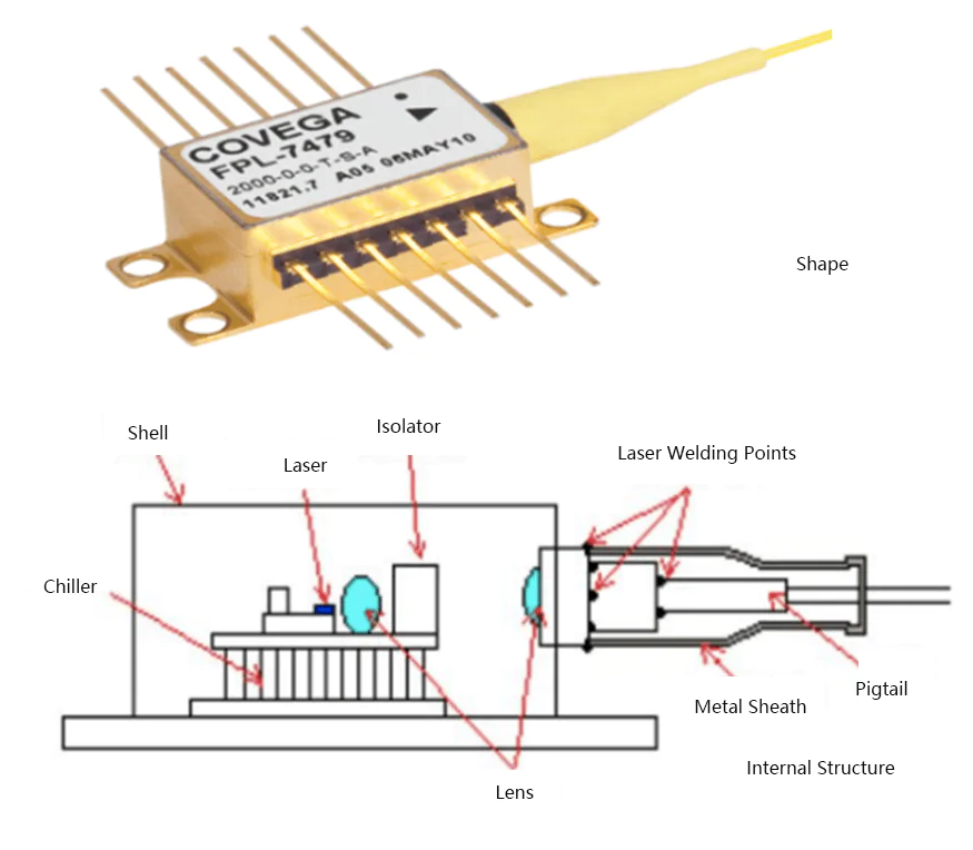
1. TO-CAN Packaging:
The laser is mounted on a small heat sink (heat dissipator) and connected to electrical pins through wires. It is then further packaged with a metal cap and a sealed window for laser emission. TO-CAN packaging is compact and relatively cost-effective. However, its drawback is that it has a small volume, making it difficult to install larger heat dissipation devices. It is not suitable for high power, high current, and long-distance scenarios. It is more suitable for applications in the telecommunications market, such as 10km 10G/25G, such as base station fronthaul and home broadband.

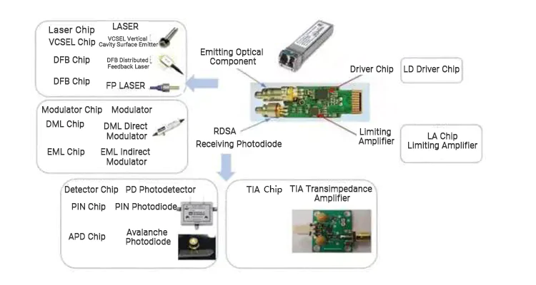
After being converted to TO-CAN, it has the basic laser packaging. However, the laser's beam diameter and the optical fiber are still different. Further alignment and coupling with lenses and optical fibers are required to focus most of the energy into the optical fiber. After complete packaging, it becomes a TOSA (Transmitting Optical Sub-Assembly). Similarly, on the other end, if it is replaced with a receiver chip, it is called ROSA (Receiver Optical Sub-Assembly). Together, they are referred to as OSA (Optical Sub-Assembly).
2. Butterfly Packaging:
To meet high-power requirements, butterfly packaging can be used. The laser is mounted on a larger heat sink (which can also include temperature control using TEC). Optical components such as lenses and isolators are also installed within the metal casing. Butterfly packaging integrates the laser and the entire optical path. Categorically, a butterfly packaged device is a higher-level component compared to TO-CAN.
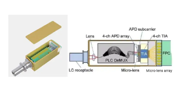
3. BOX Packaging:
BOX packaging is a special form of butterfly packaging mainly designed for multi-channel requirements. We will discuss multi-channels in detail later. In this packaging, multiple lasers are integrated within a single package, and transmission is achieved through a single optical fiber. This packaging is suitable for applications that require high temperature control, air tightness, and reliability.
Non-Hermetic Packaging
Since the widespread use of optical transceivers in the data center market, the overall working environment has been significantly optimized compared to the telecommunications market, which is exposed to outdoor conditions such as wind and sun, due to the installation of air conditioning, environmental monitoring, and other equipment in data centers.
At the same time, there is a high demand for cost control due to the large quantity of optical transceivers used. As a result, non-hermetic packaging has gradually emerged. The technology of non-hermetic packaging has been continuously iterated, leading to rapid improvements in reliability, and its applicability in various scenarios is increasing.
Non-hermetic packaging, in simple terms, refers to directly attaching/welding the optical chip to the circuit board and providing simple sealing protection using epoxy resin or other adhesives. This approach reduces the need for a large number of auxiliary components, resulting in cost savings and increased integration.
One example of non-hermetic packaging is Chip-on-Board (COB) packaging. COB packaging involves attaching the laser chip to a PCB substrate and integrating components such as laser arrays and receiver arrays in a small space to achieve miniaturization. By reducing certain protective measures and the number of auxiliary components, the cost is relatively lower compared to other packaging methods.
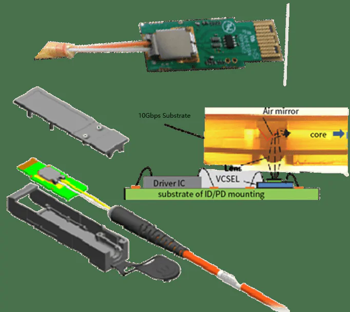
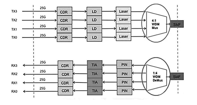
25G and below rate optical transceivers often use single-channel TO or butterfly packaged optical transceiver components that are soldered onto PCB boards to form the optical module. However, for high-speed optical transceivers with rates of 40G and above, they are primarily implemented through multi-channel parallelization due to the limitations of laser rates (often 25G). For example, 40G is achieved by 4x10G, while 100G is achieved by 4x25G.
The packaging of high-speed optical transceivers imposes higher requirements on parallel optical design, high-speed electromagnetic interference, size reduction, and increased power dissipation and heat dissipation issues. COB packaging can integrate TIA/LA chips, laser arrays, and receiver arrays into a small space to achieve miniaturization.
In summary, hermetic packaging uses metal and glass to provide tight protection for fragile optical chips, enabling them to withstand various usage environments. There are several specific packaging methods based on different device design requirements. However, the overall device complexity and the need for a costly flexible printed circuit (FPC), also known as a "flex board," to route high-frequency signals out of the hermetic enclosure, result in higher costs. In cases where the working environment is relatively controllable and the reliability requirements can be met, non-hermetic packaging can optimize costs.
Selection of Optical Chips
There are multiple chip options available based on considerations such as transmission distance, modulation scheme, and cost. When selecting optical chips, supply chain considerations are also important. Popular products often experience shortages during the initial production phase, and instances of delays and delivery postponements are common.
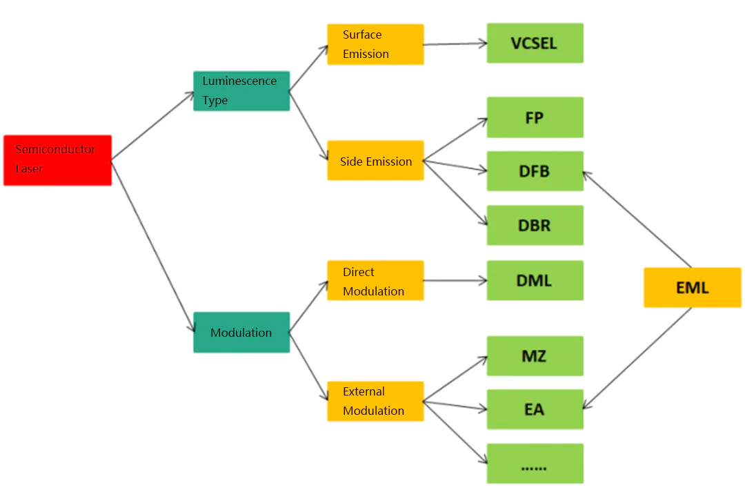
VCSEL
VCSEL (Vertical-Cavity Surface-Emitting Laser) chips are the lowest-cost option. However, they have a larger emitting angle and are typically used with relatively thick multimode fibers. Considering the overall system cost, VCSEL chips are commonly applied in short-distance scenarios such as a few meters for AOC (Active Optical Cable) and around 100 meters for SR (Short Reach) optical transceivers.
DFB
DFB (Distributed Feedback) chips are processed with gratings on original FP (Fabry-Perot) lasers, enabling more precise wavelength selection and higher output wavelength accuracy. DFB chips have a smaller emitting angle, allowing for more efficient optical coupling. Therefore, they are widely used in medium to long-distance applications, such as 500 meters or 2 kilometers, and offer a relatively moderate cost.
EML
EML (Electro-absorption Modulated Laser) chips are one of the highest-cost options. They consist of an emitting chip (which can be DFB/DBR, etc.) combined with an external absorption modulator. During operation, the laser chip remains in an emitting state, and the EML laser's signal output is controlled by switching the modulator's absorption (simply put, it can be transparent or opaque).
Now, let's explain what happens during the transmission of optical signals.
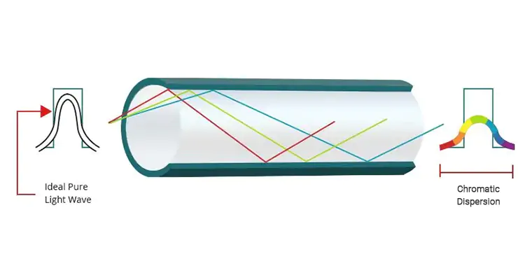
1. Light of different wavelengths travels at different speeds in optical fibers.
2. When the laser chip is powered on and emits light, there is a slight wavelength variation (chirping) that occurs within a femtosecond-level micro-timescale.
Based on these two phenomena, when a DFB chip receives an electrical signal, it emits a laser signal (which contains a certain range of wavelength components). During long-distance transmission through optical fibers, dispersion occurs, meaning that signals of different wavelengths arrive at the receiving end with significant time differences, potentially causing interference.
In the example shown in the figure below, two pulse signals are emitted from the DFB laser transmitter. Due to the different transmission speeds of different wavelengths in the optical fiber, the arrival times at the receiving end differ. In severe cases, the two pulse signals can mix together (inter-symbol interference), resulting in communication failure.
The advantage of using EML (Electro-absorption Modulated Laser) lasers is that the laser chip operates in a stable state, resulting in a "purer" emitted wavelength. Even after modulation through an external modulator and long-distance transmission, the signal quality remains high. Therefore, EML is suitable for long-distance transmission applications (10km, 20km, 40km, or even longer).
However, due to the addition of an external absorption modulator and the higher overall quality requirements for chips in long-distance scenarios, EML chips of the same speed have a cost that is 50% or even several times higher than DFB chips.
On the other hand, the response speed of the external absorption modulator is higher compared to direct modulation of DFB lasers, making it more suitable for certain modulation techniques such as PAM4 (which will be further discussed later).
Tunable Narrow Linewidth Lasers (referred to as "Tunable Lasers")
As mentioned earlier, long-distance transmission is affected by dispersion, and EML lasers can address the chirping issue. However, the inherent emission wavelength range (referred to as "linewidth") of lasers still exists, and dispersion remains a challenge in applications like ultra-long-haul ODN (Optical Distribution Network) spanning 80km, 100km, or even longer distances.
On the other hand, for long-haul backbone transmission, overall system cost needs to be considered. Therefore, Dense Wavelength Division Multiplexing (DWDM) technology is introduced to transmit signals of different wavelengths over a single fiber, greatly increasing the transmission capacity of a single fiber and reducing the overall system cost of long-haul backbone networks. To meet these two requirements, tunable narrow linewidth lasers are used.
Tunable narrow linewidth laser structures are more complex, and there are various approaches, including current control, temperature control, mechanical control, and more. Taking the example of an external cavity mechanical control scheme, a grating structure is added to the ordinary laser, and the output wavelength is adjusted through mechanical control to achieve more precise wavelength control.
In the past, tunable lasers had relatively limited applications. However, with the potential introduction of wavelength division multiplexing (WDM) technology in 5G fronthaul, some manufacturers are also exploring the possibilities of using tunable lasers. Future demand may see significant changes.
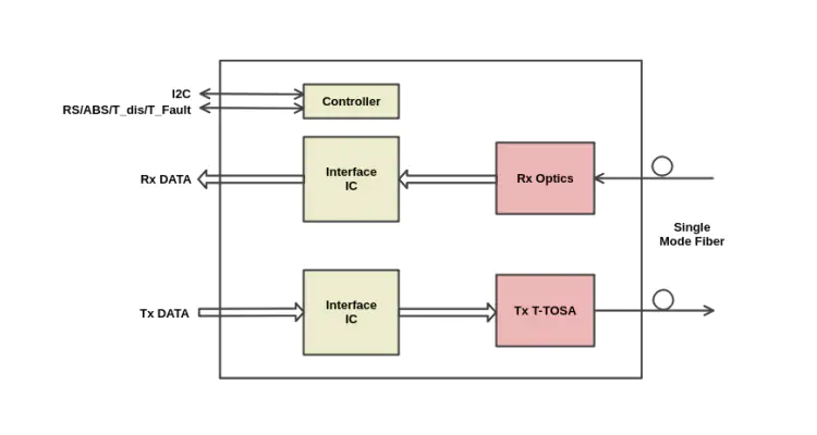
For this reason, NADDOD provides the Tunable SFP+/XFP 10G DWDM 80km Optical Transceiver, which can meet the current needs of 5G fronthaul WDM applications. The schematic diagram of the module's principle is as follows:
In summary, VCSEL chips are chosen for low-cost short-distance applications, DFB chips for medium-distance applications, EML chips for medium to long-distance and special modulation requirements, and tunable narrow linewidth lasers for ultra-long distances and certain specific applications.
Conclusion
In conclusion, the design and manufacturing of optical transceivers are complex and critical processes. When analyzing the requirements for transceivers, consideration should be given to the choice between hermetic and non-hermetic packaging, as well as the characteristics and application scenarios of different types of optical chips.
Through appropriate packaging selection and matching of optical chip types, efficient, stable, and reliable optical transceiver designs can be achieved to meet communication needs in various fields. In the future, with the continuous development of optical communication technology, we can expect more innovations and breakthroughs that will bring greater possibilities for optical module design.